CHAPTER 6 Digital Communication Part 1 Introduction to



- Slides: 86

CHAPTER - 6 Digital Communication Part -1 Introduction to Digital Modulation Sampling theorem Pulse Analog Modulation Delta Modulation Prepared by Dr M. Murugappan

Topics Covered in this chapter Introduction to Digital Modulation Sampling theorem Pulse Analog Modulation Pulse Amplitude Modulation Pulse Width Modulation Pulse Position Modulation Pulse Code Modulation Delta Modulation Line coding Amplitude Shift Keying (ASK) Frequency Shift Keying (FSK) Time-Division Multiplexing (TDM) Frequency Division Multiplexing (FDM)

Introduction ü Transfer of information in digital form ü Digital Communication Vs Data Communication ü In the early 90’s, telecommunication networks is changing towards digital world. ü With the rapid advancement in the field of microprocessor, several telecommunication components such as transmission line and switching have used digital signals in their operation. ü Therefore, information signals must be changed to digital form so that it can be transmitted through this network. - ü Several techniques requiring full coding of the original signal will be used: • Pulse Code Modulation (PCM) • Delta Modulation (DM)

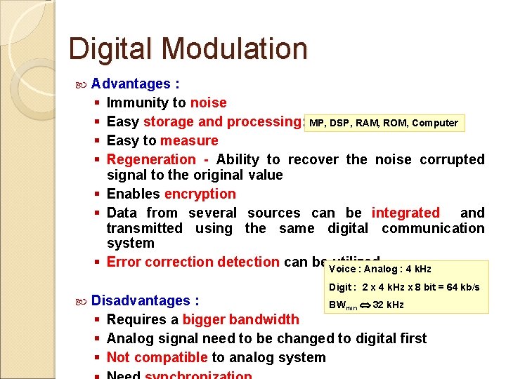
Digital Modulation Advantages : § Immunity to noise § Easy storage and processing: MP, DSP, RAM, ROM, Computer § Easy to measure § Regeneration - Ability to recover the noise corrupted signal to the original value § Enables encryption § Data from several sources can be integrated and transmitted using the same digital communication system § Error correction detection can be Voice utilized : Analog : 4 k. Hz Digit : 2 x 4 k. Hz x 8 bit = 64 kb/s Disadvantages : BWmin 32 k. Hz § Requires a bigger bandwidth § Analog signal need to be changed to digital first § Not compatible to analog system

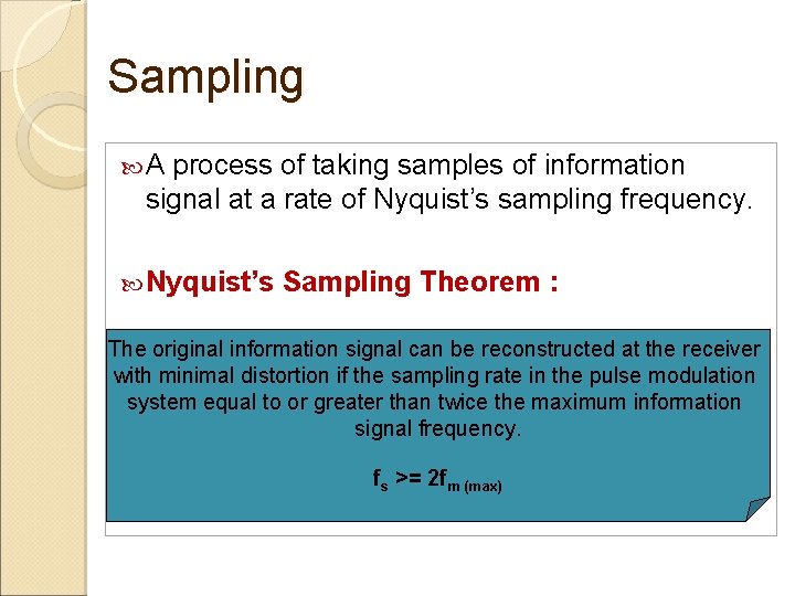
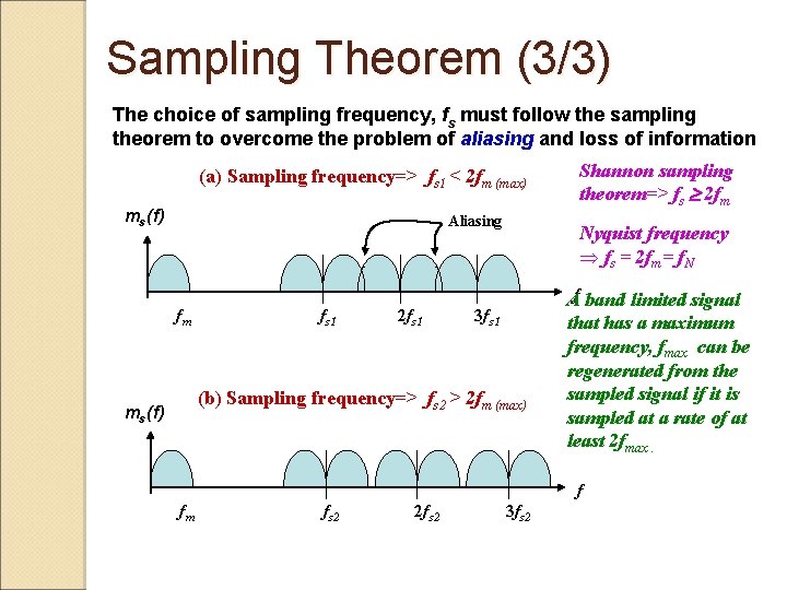
Sampling A process of taking samples of information signal at a rate of Nyquist’s sampling frequency. Nyquist’s Sampling Theorem : The original information signal can be reconstructed at the receiver with minimal distortion if the sampling rate in the pulse modulation system equal to or greater than twice the maximum information signal frequency. fs >= 2 fm (max)

Types of Sampling Two basic techniques used to perform the sampling function: § Natural sampling § Flat-top sampling

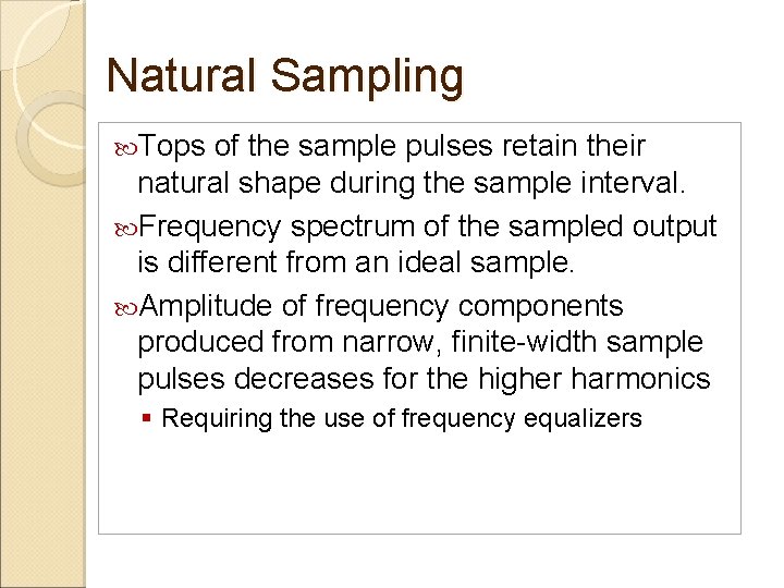
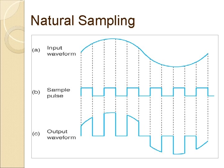
Natural Sampling Tops of the sample pulses retain their natural shape during the sample interval. Frequency spectrum of the sampled output is different from an ideal sample. Amplitude of frequency components produced from narrow, finite-width sample pulses decreases for the higher harmonics § Requiring the use of frequency equalizers

Natural Sampling

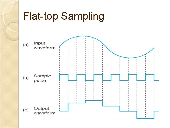
Flat-top Sampling Common used in PCM systems. Accomplish in a sample-and-hold circuit § To periodically sample the continually changing analog input voltage & convert to a series of constant-amplitude PAM voltage levels. The input voltage is sampled with a narrow pulse and then held relatively constant until the next sample is taken.

Flat-top Sampling process alters the frequency spectrum & introduces aperture error. The amplitude of the sampled signal changes during the sample pulse time. Advantages: § Introduces less aperture distortion § Can operate with a slower ADC

Flat-top Sampling

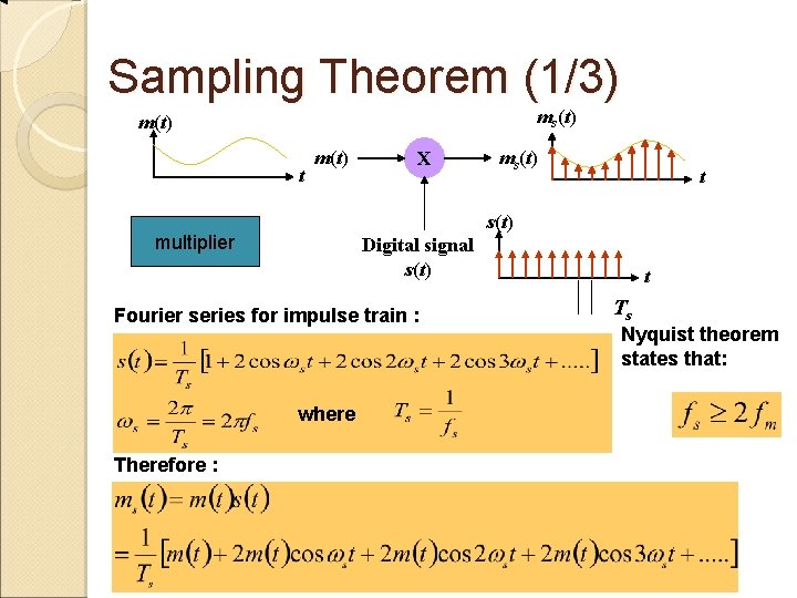
Sampling Theorem (1/3) ms(t) m(t) t m(t) X t s(t) multiplier Digital signal s(t) Fourier series for impulse train : where Therefore : ms(t) t Ts Nyquist theorem states that:

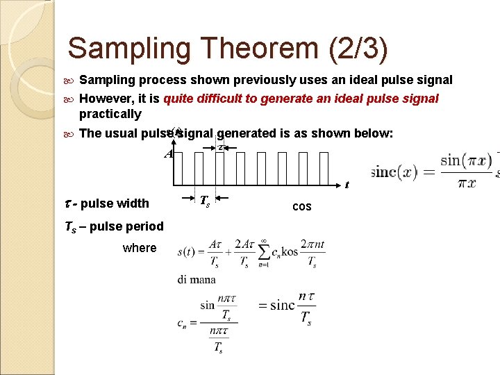
Sampling Theorem (2/3) Sampling process shown previously uses an ideal pulse signal However, it is quite difficult to generate an ideal pulse signal practically s(t)signal generated is as shown below: The usual pulse A t - pulse width Ts – pulse period where Ts cos

Sampling Theorem (3/3) The choice of sampling frequency, fs must follow the sampling theorem to overcome the problem of aliasing and loss of information (a) Sampling frequency=> fs 1 < 2 fm (max) ms(f) Aliasing fm fs 1 2 fs 1 Nyquist frequency Þ fs = 2 fm= f. N 3 fs 1 (b) Sampling frequency=> fs 2 > 2 fm (max) ms(f) Shannon sampling theorem=> fs 2 fm Af band limited signal that has a maximum frequency, fmax can be regenerated from the sampled signal if it is sampled at a rate of at least 2 fmax. f fm fs 2 2 fs 2 3 fs 2

Pulse Modulation (1/2) Sampling analog information signal Converting samples into discrete pulses Transport the pulses from source to destination over physical transmission medium.

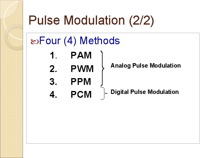
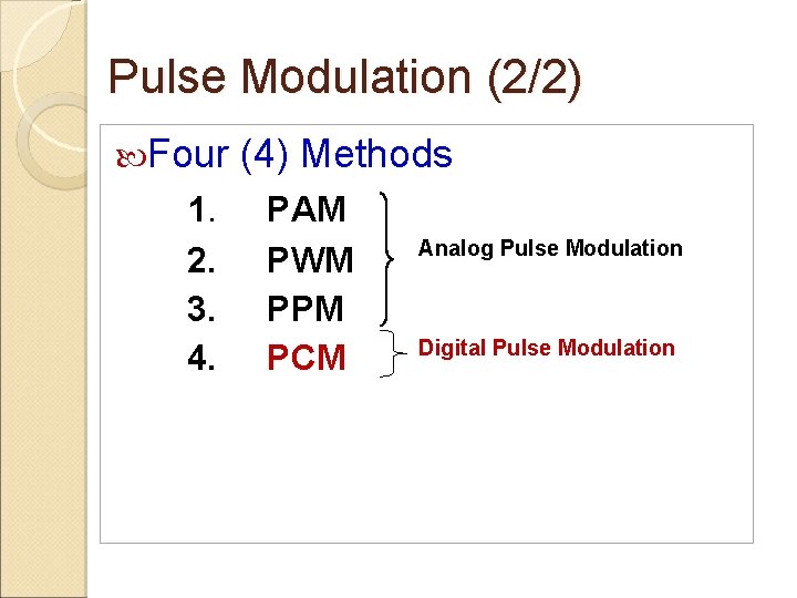
Pulse Modulation (2/2) Four 1. 2. 3. 4. (4) Methods PAM PWM PPM PCM Analog Pulse Modulation Digital Pulse Modulation

Pulse Modulation (2/2) Four 1. 2. 3. 4. (4) Methods PAM PWM PPM PCM Analog Pulse Modulation Digital Pulse Modulation

Pulse Code Modulation (PCM) Basic § § scheme of PCM system Quantization Error Companding Block diagram & function of TDM-PCM communication system

Basic scheme of PCM system The most common technique for using digital signals to encode analog data is PCM. Example: To transfer analog voice signals off a local loop to digital end office within the phone system, one uses a codec.

Basic scheme of PCM system Because voice data limited to frequencies below 4000 Hz, a codec makes 8000 samples/sec. (i. e. , 125 microsecond/sample). If a signal is sampled at regular intervals at a rate higher than twice the highest signal frequency, the samples contain all the information of the original signal. Definition: PCM is essentially analog-to-digital conversion of a special type where the information contained in the instantaneous samples of an analog signal is represented by digital words in a serial bit

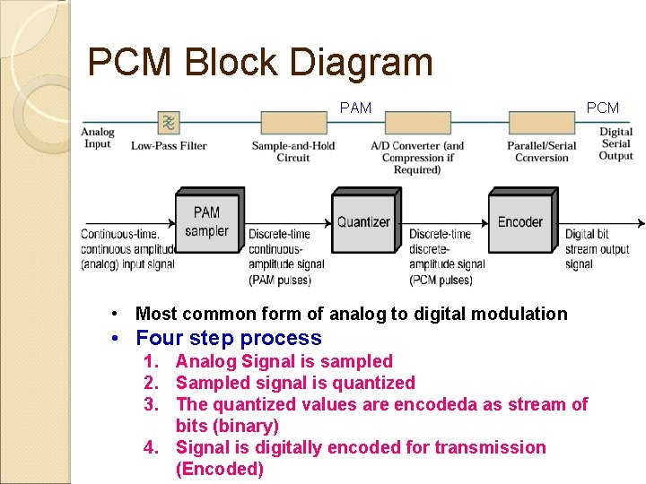
PCM Block Diagram PAM PCM • Most common form of analog to digital modulation • Four step process 1. Analog Signal is sampled 2. Sampled signal is quantized 3. The quantized values are encodeda as stream of bits (binary) 4. Signal is digitally encoded for transmission (Encoded)

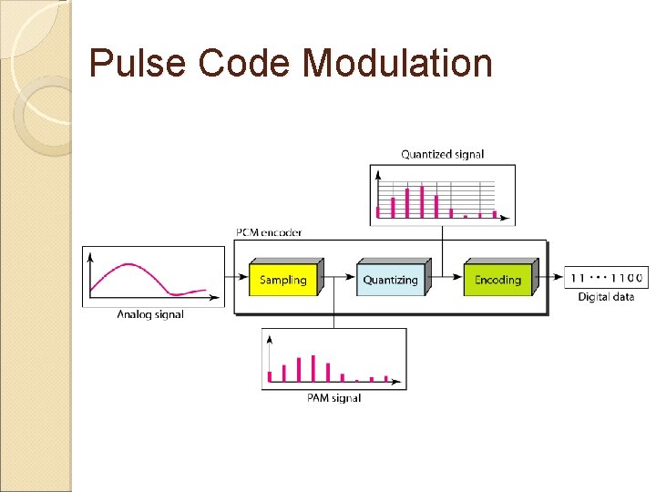
Pulse Code Modulation

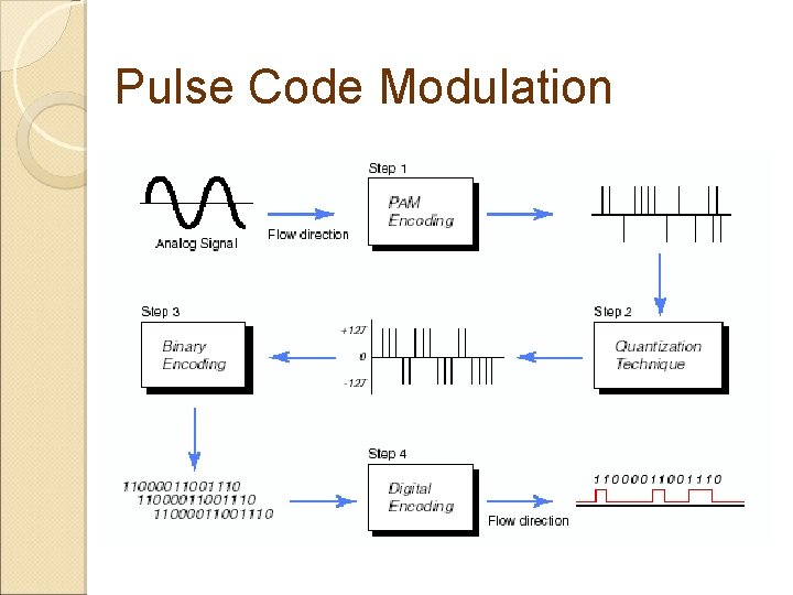
Pulse Code Modulation

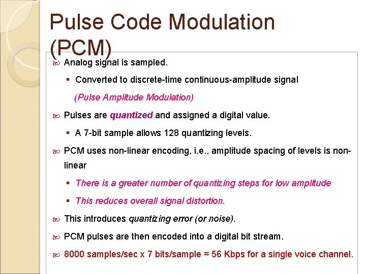
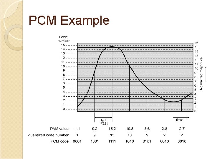
Pulse Code Modulation (PCM) Analog signal is sampled. § Converted to discrete-time continuous-amplitude signal (Pulse Amplitude Modulation) Pulses are quantized and assigned a digital value. § A 7 -bit sample allows 128 quantizing levels. PCM uses non-linear encoding, i. e. , amplitude spacing of levels is nonlinear § There is a greater number of quantizing steps for low amplitude § This reduces overall signal distortion. This introduces quantizing error (or noise). PCM pulses are then encoded into a digital bit stream. 8000 samples/sec x 7 bits/sample = 56 Kbps for a single voice channel.

PCM Example

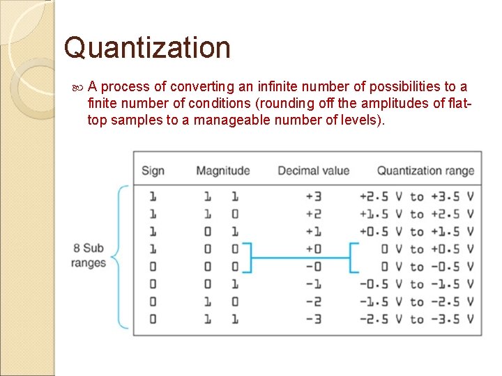
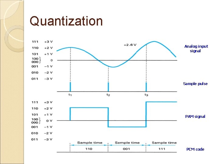
Quantization A process of converting an infinite number of possibilities to a finite number of conditions (rounding off the amplitudes of flattop samples to a manageable number of levels).

Quantization Analog input signal Sample pulse PAM signal PCM code

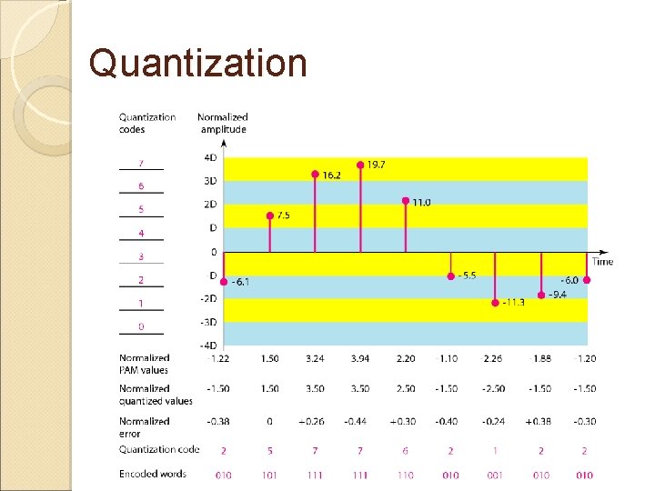
Quantization

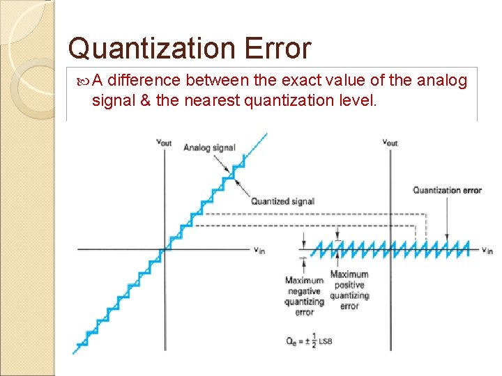
Quantization Error A difference between the exact value of the analog signal & the nearest quantization level.

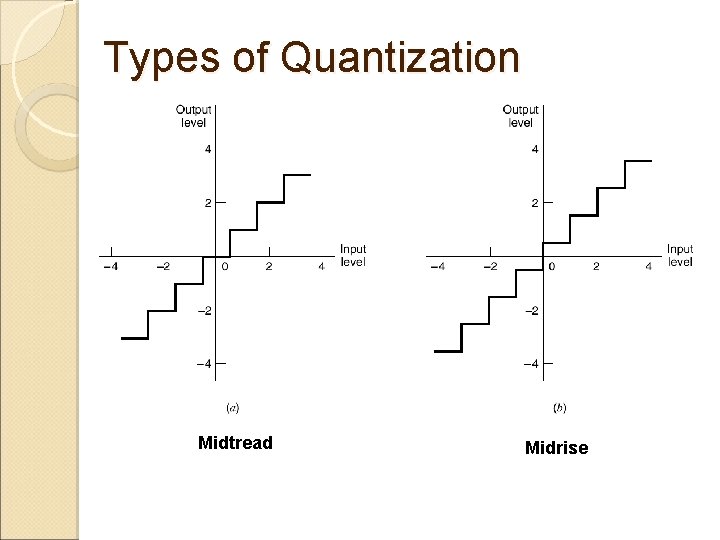
Types of Quantization Midtread Midrise

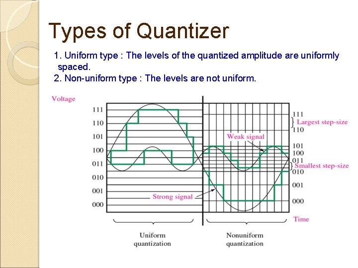
Types of Quantizer 1. Uniform type : The levels of the quantized amplitude are uniformly spaced. 2. Non-uniform type : The levels are not uniform.

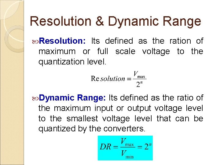
Resolution & Dynamic Range Resolution: Its defined as the ration of maximum or full scale voltage to the quantization level. Dynamic Range: Its defined as the ratio of the maximum input or output voltage level to the smallest voltage level that can be quantized by the converters.

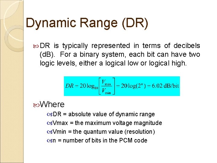
Dynamic Range (DR) DR is typically represented in terms of decibels (d. B). For a binary system, each bit can have two logic levels, either a logical low or logical high. Where DR = absolute value of dynamic range Vmax = the maximum voltage magnitude Vmin = the quantum value (resolution) n = number of bits in the PCM code

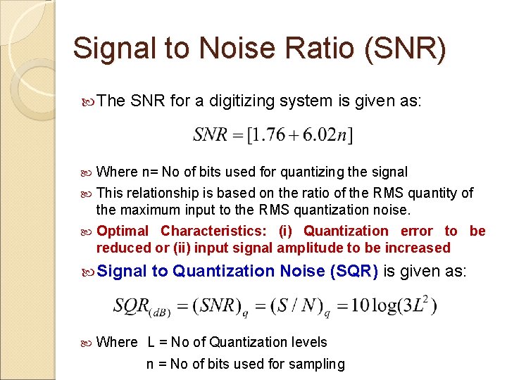
Signal to Noise Ratio (SNR) The SNR for a digitizing system is given as: Where n= No of bits used for quantizing the signal This relationship is based on the ratio of the RMS quantity of the maximum input to the RMS quantization noise. Optimal Characteristics: (i) Quantization error to be reduced or (ii) input signal amplitude to be increased Signal to Quantization Noise (SQR) is given as: Where L = No of Quantization levels n = No of bits used for sampling

Example 1 1. A CD audio laser disk system has a frequency bandwidth of 20 Hz to 20 k. Hz. What is the minimum sample rate required to satisfy the Nyquist Sampling rate?

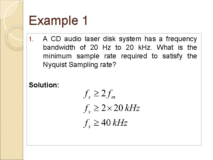
Example 1 1. A CD audio laser disk system has a frequency bandwidth of 20 Hz to 20 k. Hz. What is the minimum sample rate required to satisfy the Nyquist Sampling rate? Solution:

Example 2 1. A digitizing system specifies 55 d. B of dynamic range. How many bits are required to satisfy the dynamic range specification? What is the signal to noise ratio for the system? What is SQR for the system?

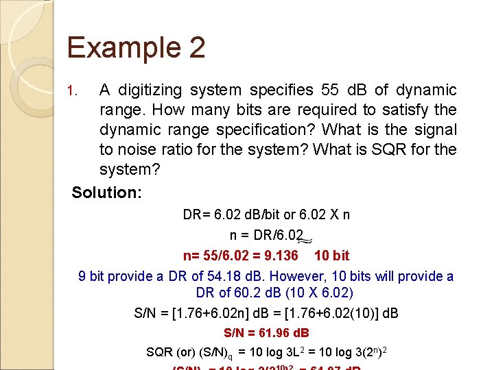
Example 2 A digitizing system specifies 55 d. B of dynamic range. How many bits are required to satisfy the dynamic range specification? What is the signal to noise ratio for the system? What is SQR for the system? Solution: 1. DR= 6. 02 d. B/bit or 6. 02 X n n = DR/6. 02 n= 55/6. 02 = 9. 136 10 bit 9 bit provide a DR of 54. 18 d. B. However, 10 bits will provide a DR of 60. 2 d. B (10 X 6. 02) S/N = [1. 76+6. 02 n] d. B = [1. 76+6. 02(10)] d. B S/N = 61. 96 d. B SQR (or) (S/N)q = 10 log 3 L 2 = 10 log 3(2 n)2

Non-Linear Coding Quantization Reduces Can levels not evenly spaced overall signal distortion also be done by Companding

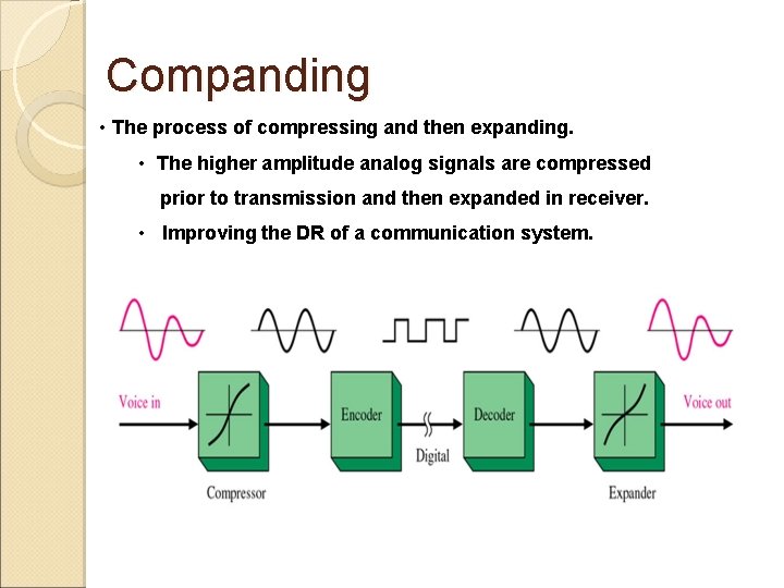
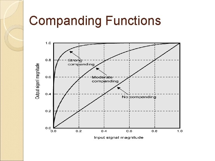
Companding • The process of compressing and then expanding. • The higher amplitude analog signals are compressed prior to transmission and then expanded in receiver. • Improving the DR of a communication system.

Companding Functions

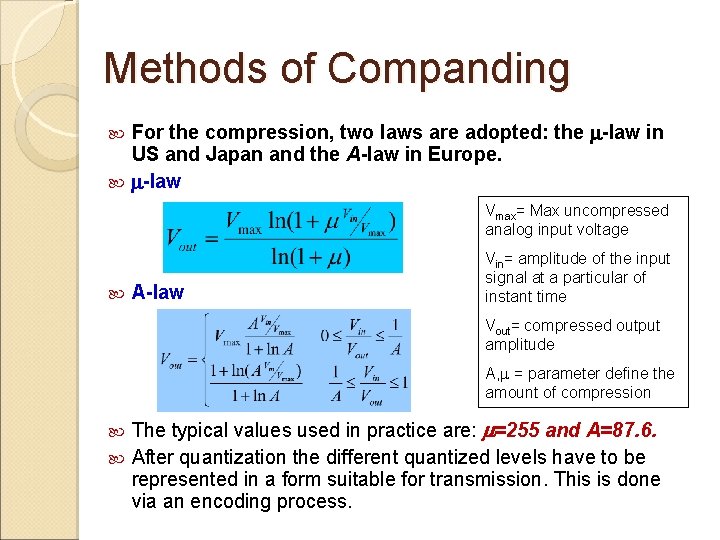
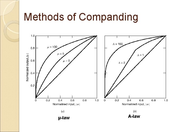
Methods of Companding For the compression, two laws are adopted: the -law in US and Japan and the A-law in Europe. -law Vmax= Max uncompressed analog input voltage A-law Vin= amplitude of the input signal at a particular of instant time Vout= compressed output amplitude A, = parameter define the amount of compression The typical values used in practice are: =255 and A=87. 6. After quantization the different quantized levels have to be represented in a form suitable for transmission. This is done via an encoding process.

Methods of Companding μ-law A-law

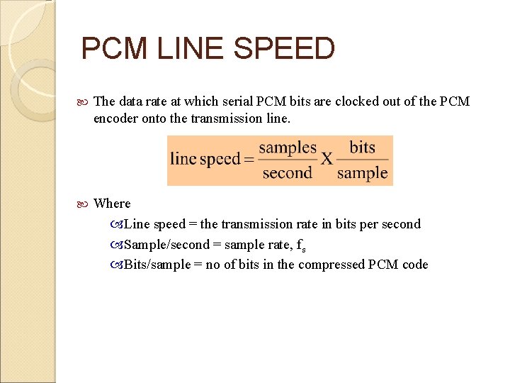
PCM LINE SPEED The data rate at which serial PCM bits are clocked out of the PCM encoder onto the transmission line. Where Line speed = the transmission rate in bits per second Sample/second = sample rate, fs Bits/sample = no of bits in the compressed PCM code

Advantages of PCM The most important advantages of PCM are: § Robustness to channel noise and interference. § Efficient regeneration of the coded signal along the channel path. § Efficient exchange between Bt and SNR. § Uniformat for different kind of baseband signals.

DELTA MODULATION (DM)

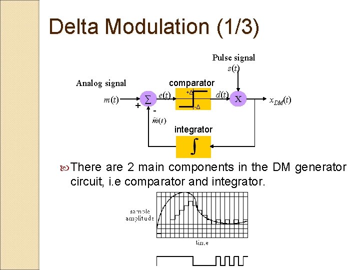
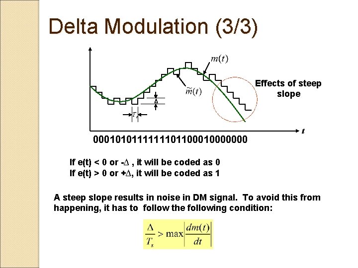
Delta Modulation (1/3) Pulse signal s(t) Analog signal m(t) comparator +Δ d(t) X e(t) ∑ + -Δ - x. DM(t) integrator There are 2 main components in the DM generator circuit, i. e comparator and integrator.

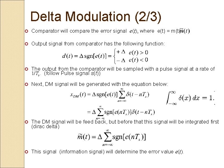
Delta Modulation (2/3) Comparator will compare the error signal e(t), where e(t) = m(t) - Output signal from comparator has the following function: The output from the comparator will be sampled with a pulse signal at a rate of 1/Ts. (follow Pulse signal s(t)) Next, DM signal will be generated with the equation below: The DM signal will be feed back, but before that this signal will be integrated first (dirac delta) This signal (information signal) will determine the error value e(t).

Delta Modulation (3/3) Δ Effects of steep slope Ts 000101011111110110000000 t If e(t) < 0 or -∆ , it will be coded as 0 If e(t) > 0 or +∆, it will be coded as 1 A steep slope results in noise in DM signal. To avoid this from happening, it has to follow the following condition:

Delta Modulation Its also called “Slope Modulation” or “Tracking ADC”. § Because, the output of DM is follows the contour changes of the input waveform. Simple modulation technique compared to PCM § No parallel to serial converters are required Highly suitable for voice communication Dis-advantage: § Not suitable for “slope overload” – High rate of change of input signal Continuous variable slope delta (CVSD) modulation

LINE CODING

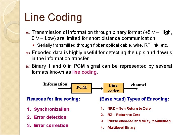
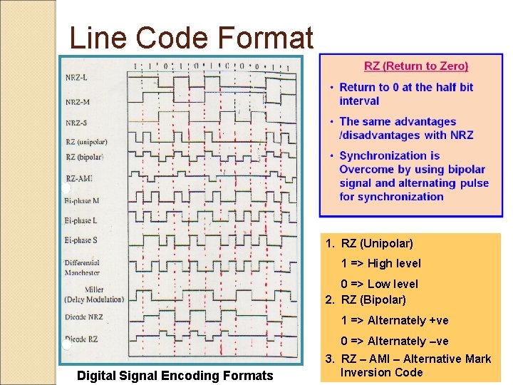
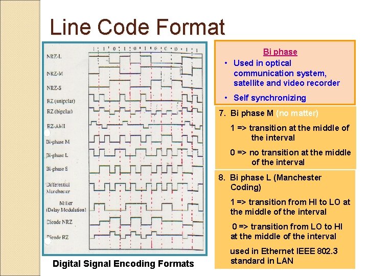
Line Coding Transmission of information through binary format (+5 V – High, 0 V – Low) are limited for short distance communication. § Serially transmitted through fibber optical cable, wire, RF link, etc. Encoded data is highly useful for detecting the up’s and down’s in the information transfer. Binary 1 and 0 in PCM signal can be represented by several formats known as line coding. Information Line coder PCM channel Reasons for line coding: (Base band) Types of Encoding: 1. Synchronization 1. NRZ – Non Return to Zero 2. RZ – Return to Zero 3. Phase encoded and delay modulation 4. Multilevel Binary 2. Error detection 3. Error correction

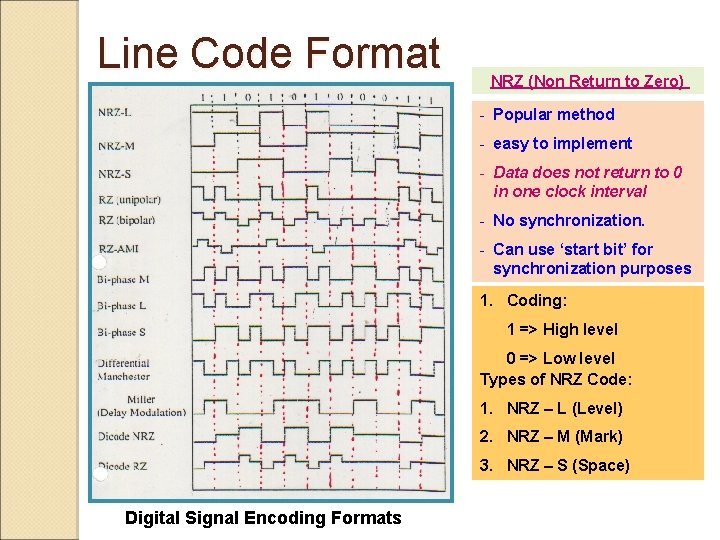
Line Code Format NRZ (Non Return to Zero) - Popular method - easy to implement - Data does not return to 0 in one clock interval - No synchronization. - Can use ‘start bit’ for synchronization purposes 1. Coding: 1 => High level 0 => Low level Types of NRZ Code: 1. NRZ – L (Level) 2. NRZ – M (Mark) 3. NRZ – S (Space) Digital Signal Encoding Formats

Line Code Format 1. RZ (Unipolar) 1 => High level 0 => Low level 2. RZ (Bipolar) 1 => Alternately +ve 0 => Alternately –ve Digital Signal Encoding Formats 3. RZ – AMI – Alternative Mark Inversion Code

Line Code Format Bi phase • Used in optical communication system, satellite and video recorder • Self synchronizing 7. Bi phase M (no matter) 1 => transition at the middle of the interval 0 => no transition at the middle of the interval 8. Bi phase L (Manchester Coding) 1 => transition from HI to LO at the middle of the interval 0 => transition from LO to HI at the middle of the interval Digital Signal Encoding Formats used in Ethernet IEEE 802. 3 standard in LAN

AMPLITUDE SHIFT KEYING (ASK) FREQUENY SHIFT KEYING (FSK) PHASE SHIFT KEYING (PSK)

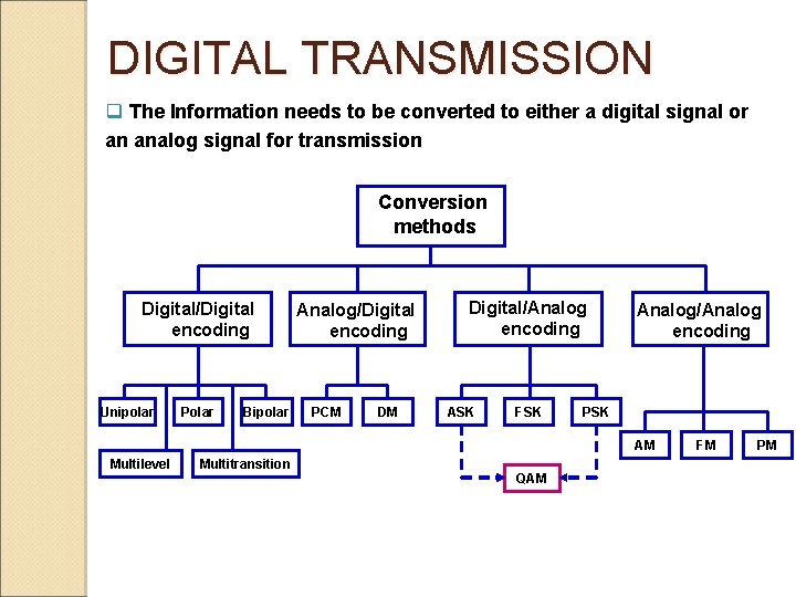
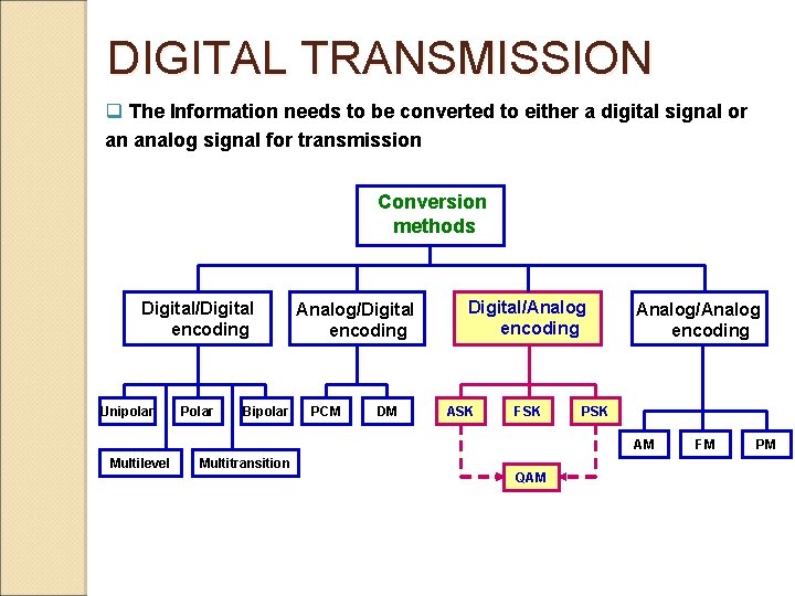
DIGITAL TRANSMISSION q The Information needs to be converted to either a digital signal or an analog signal for transmission Conversion methods Digital/Digital encoding Unipolar Polar Bipolar Analog/Digital encoding PCM DM Digital/Analog encoding ASK FSK Analog/Analog encoding PSK AM Multilevel Multitransition QAM FM PM

DIGITAL TRANSMISSION q The Information needs to be converted to either a digital signal or an analog signal for transmission Conversion methods Digital/Digital encoding Unipolar Polar Bipolar Analog/Digital encoding PCM DM Digital/Analog encoding ASK FSK Analog/Analog encoding PSK AM Multilevel Multitransition QAM FM PM

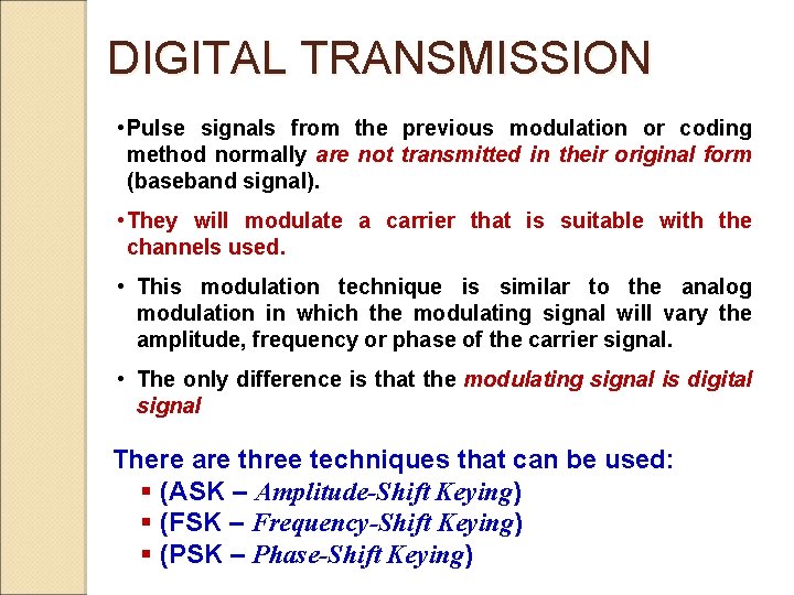
DIGITAL TRANSMISSION • Pulse signals from the previous modulation or coding method normally are not transmitted in their original form (baseband signal). • They will modulate a carrier that is suitable with the channels used. • This modulation technique is similar to the analog modulation in which the modulating signal will vary the amplitude, frequency or phase of the carrier signal. • The only difference is that the modulating signal is digital signal There are three techniques that can be used: § (ASK – Amplitude-Shift Keying) § (FSK – Frequency-Shift Keying) § (PSK – Phase-Shift Keying)

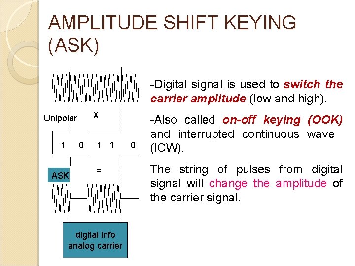
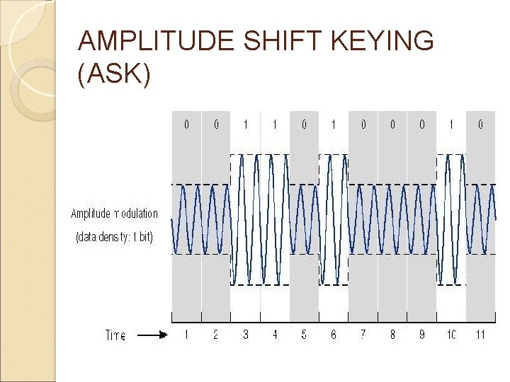
AMPLITUDE SHIFT KEYING (ASK) -Digital signal is used to switch the carrier amplitude (low and high). X Unipolar 0 1 ASK 1 1 = digital info analog carrier 0 -Also called on-off keying (OOK) and interrupted continuous wave (ICW). The string of pulses from digital signal will change the amplitude of the carrier signal.

AMPLITUDE SHIFT KEYING (ASK)

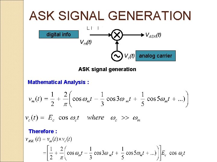
ASK SIGNAL GENERATION digital info VASK(t) Vm(t) Vc(t) analog carrier ASK signal generation Mathematical Analysis : Therefore :

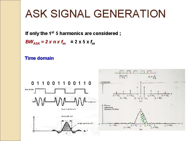
ASK SIGNAL GENERATION If only the 1 st 5 harmonics are considered ; BWASK = 2 x n x fm = 2 x 5 x fm Time domain 0 1 1 0 Spectrum of ASK signal

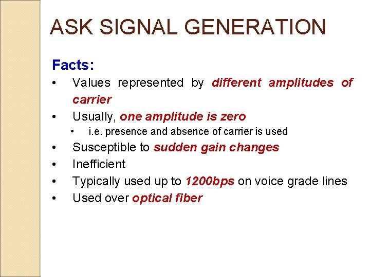
ASK SIGNAL GENERATION Facts: • • Values represented by different amplitudes of carrier Usually, one amplitude is zero • • • i. e. presence and absence of carrier is used Susceptible to sudden gain changes Inefficient Typically used up to 1200 bps on voice grade lines Used over optical fiber

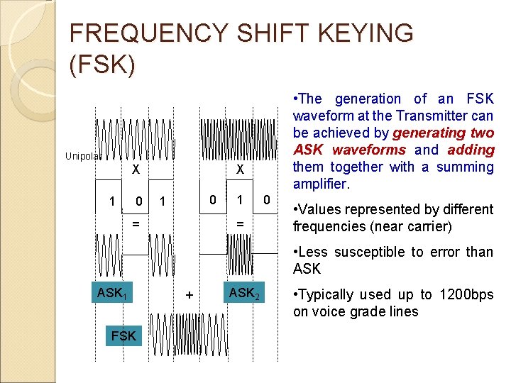
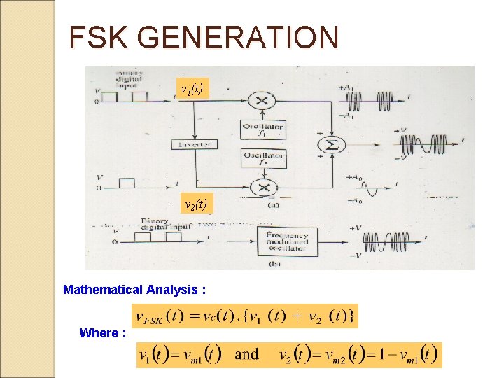
FREQUENCY SHIFT KEYING (FSK) • The generation of an FSK waveform at the Transmitter can be achieved by generating two ASK waveforms and adding them together with a summing amplifier. Unipolar X 1 0 X 0 1 = 0 • Values represented by different frequencies (near carrier) • Less susceptible to error than ASK 1 FSK + ASK 2 • Typically used up to 1200 bps on voice grade lines

FSK GENERATION v 1(t) v 2(t) Mathematical Analysis : Where :

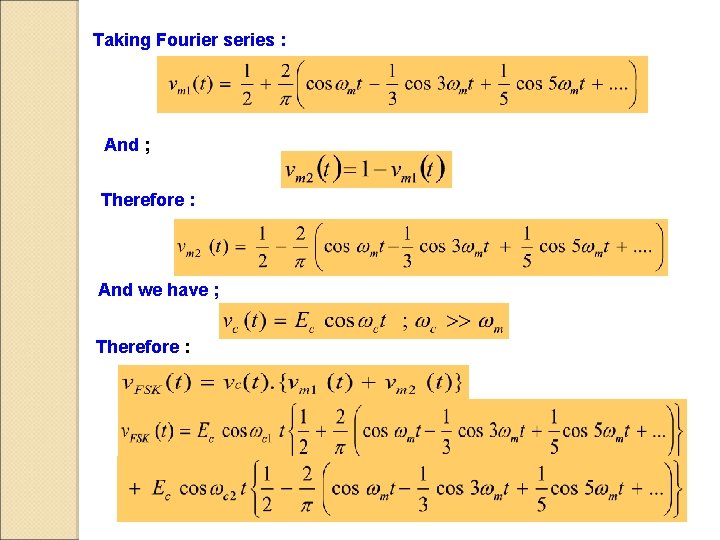
Taking Fourier series : And ; Therefore : And we have ; Therefore :

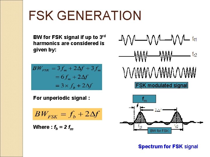
FSK GENERATION BW for FSK signal if up to 3 rd harmonics are considered is given by: FSK modulated signal For unperiodic signal : Where : fb = 2 fm fm BW for FSK Spectrum for FSK signal

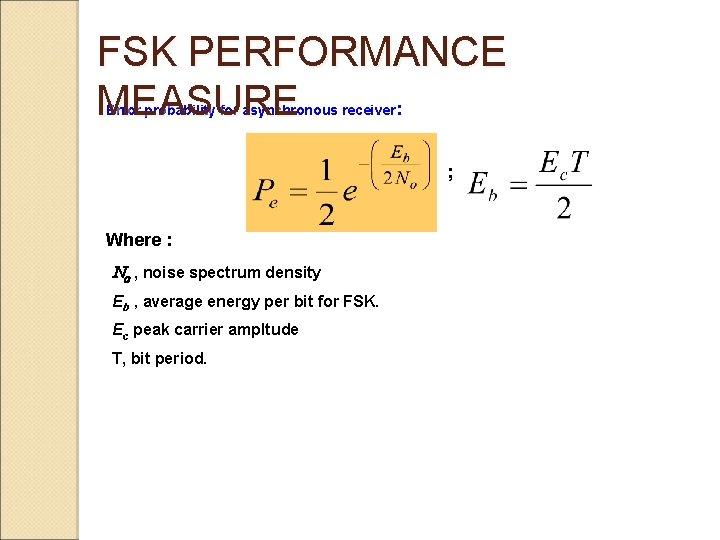
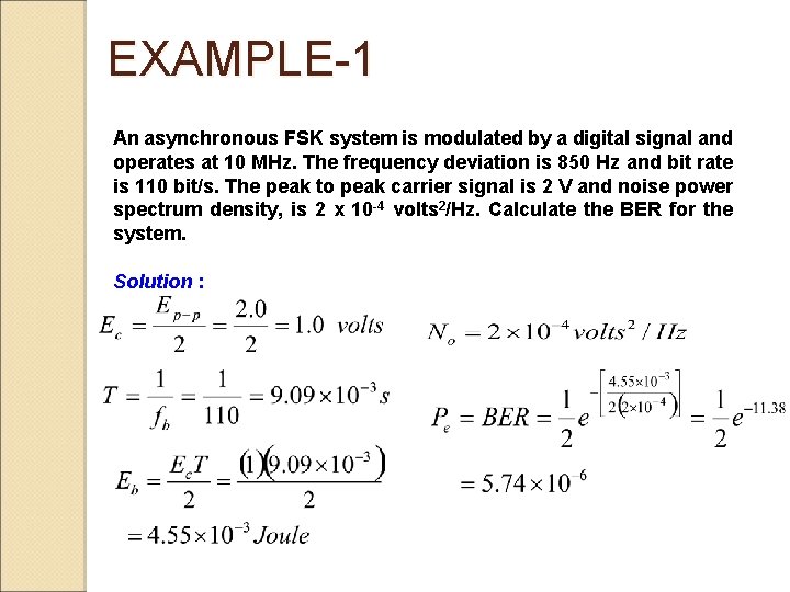
FSK PERFORMANCE MEASURE : Error probability for asynchronous receiver ; Where : No , noise spectrum density Eb , average energy per bit for FSK. Ec peak carrier ampltude T, bit period.

EXAMPLE-1 An asynchronous FSK system is modulated by a digital signal and operates at 10 MHz. The frequency deviation is 850 Hz and bit rate is 110 bit/s. The peak to peak carrier signal is 2 V and noise power spectrum density, is 2 x 10 -4 volts 2/Hz. Calculate the BER for the system. Solution :

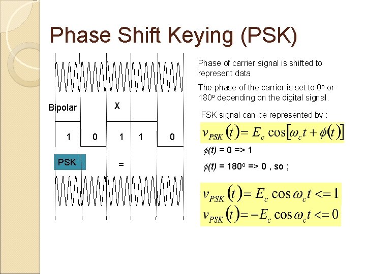
Phase Shift Keying (PSK) Phase of carrier signal is shifted to represent data X Bipolar 1 The phase of the carrier is set to 0 o or 180 o depending on the digital signal. 0 1 FSK signal can be represented by : 1 0 f(t) = 0 => 1 PSK = f(t) = 180 o => 0 , so ;

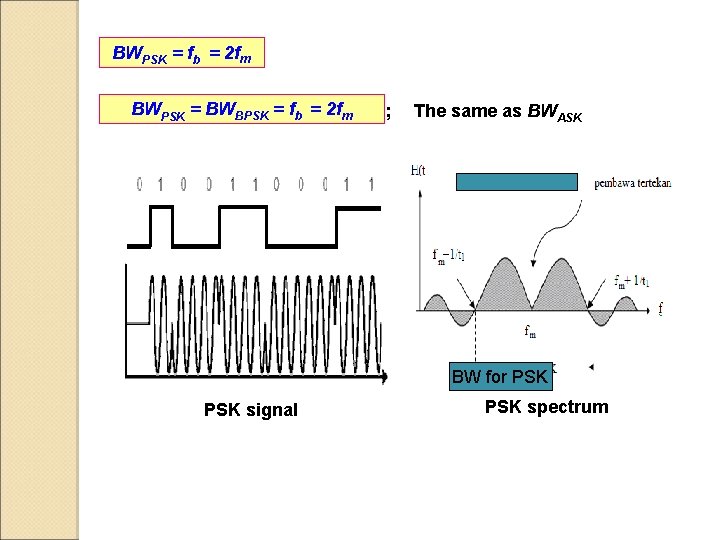
BWPSK = fb = 2 fm BWPSK = BWBPSK = fb = 2 fm ; The same as BWASK BW for PSK signal PSK spectrum

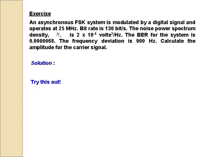
Exercise An asynchronous FSK system is modulated by a digital signal and operates at 25 MHz. Bit rate is 130 bit/s. The noise power spectrum density, is 2 x 10 -4 volts 2/Hz. The BER for the system is 0. 0000068. The frequency deviation is 900 Hz. Calculate the amplitude for the carrier signal. Solution : Try this out!

MULTIPLEXING

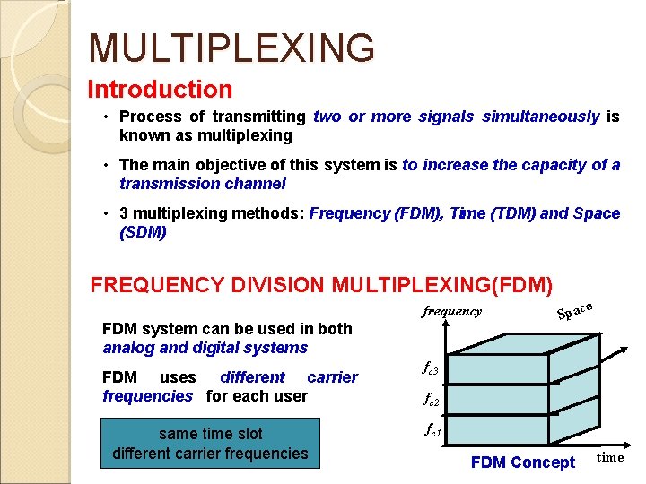
MULTIPLEXING Introduction • Process of transmitting two or more signals simultaneously is known as multiplexing • The main objective of this system is to increase the capacity of a transmission channel • 3 multiplexing methods: Frequency (FDM), Time (TDM) and Space (SDM) FREQUENCY DIVISION MULTIPLEXING(FDM) frequency FDM system can be used in both analog and digital systems FDM uses different carrier frequencies for each user same time slot different carrier frequencies e Spac fc 3 fc 2 fc 1 FDM Concept time

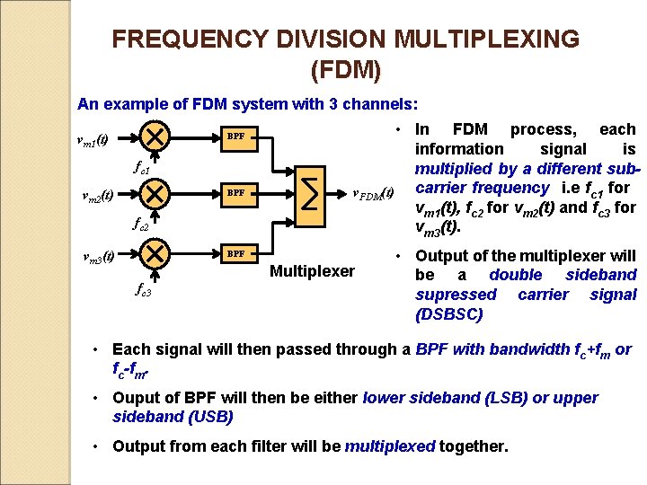
FREQUENCY DIVISION MULTIPLEXING (FDM) An example of FDM system with 3 channels: BPF vm 1(t) fc 1 vm 2(t) BPF fc 2 vm 3(t) • In FDM process, each information signal is multiplied by a different subv. FDM(t) carrier frequency i. e fc 1 for vm 1(t), fc 2 for vm 2(t) and fc 3 for vm 3(t). BPF Multiplexer fc 3 • Output of the multiplexer will be a double sideband supressed carrier signal (DSBSC) • Each signal will then passed through a BPF with bandwidth fc+fm or fc-fm. • Ouput of BPF will then be either lower sideband (LSB) or upper sideband (USB) • Output from each filter will be multiplexed together.

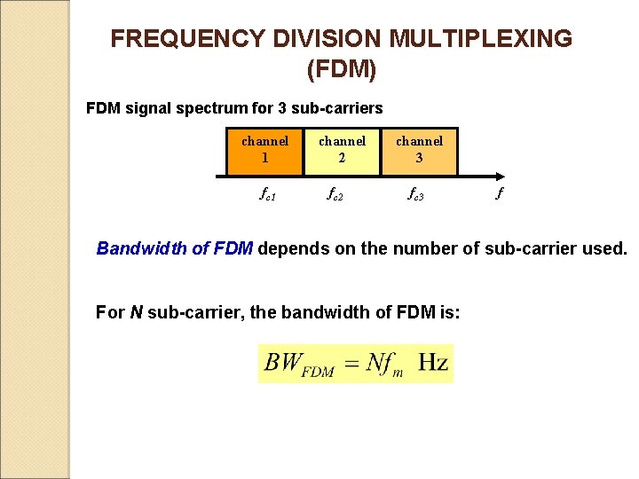
FREQUENCY DIVISION MULTIPLEXING (FDM) FDM signal spectrum for 3 sub-carriers channel 1 fc 1 channel 2 fc 2 channel 3 fc 3 f Bandwidth of FDM depends on the number of sub-carrier used. For N sub-carrier, the bandwidth of FDM is:

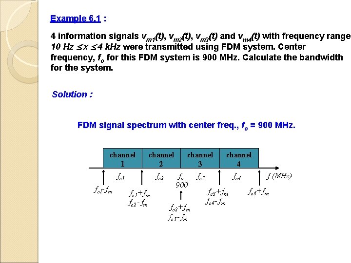
Example 6. 1 : 4 information signals vm 1(t), vm 2(t), vm 3(t) and vm 4(t) with frequency range 10 Hz x 4 k. Hz were transmitted using FDM system. Center frequency, fo for this FDM system is 900 MHz. Calculate the bandwidth for the system. Solution : FDM signal spectrum with center freq. , fo = 900 MHz. channel 1 fc 1 - fm channel 2 3 4 fc 2 fo fc 3 fc 4 f (MHz) 900 fc 4+ fm fc 3+ fm fc 1+ fm fc 4 - fm fc 2+ fm fc 3 - fm

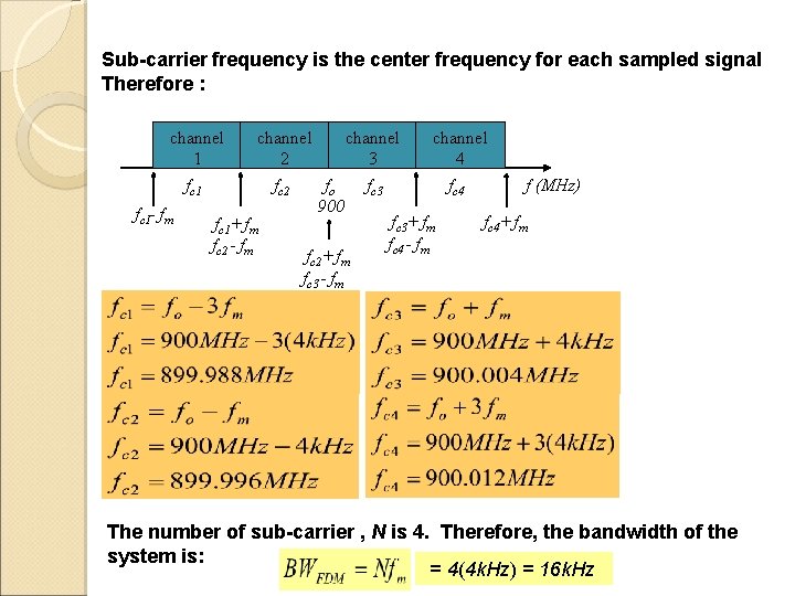
Sub-carrier frequency is the center frequency for each sampled signal Therefore : channel 1 fc 1 - fm channel 2 3 4 fc 2 fo fc 3 fc 4 f (MHz) 900 fc 3+ fm fc 4+ fm fc 1+ fm fc 4 - fm fc 2+ fm fc 3 - fm The number of sub-carrier , N is 4. Therefore, the bandwidth of the system is: = 4(4 k. Hz) = 16 k. Hz

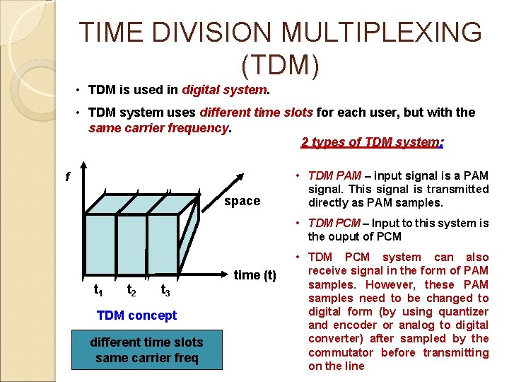
TIME DIVISION MULTIPLEXING (TDM) • TDM is used in digital system. • TDM system uses different time slots for each user, but with the same carrier frequency. 2 types of TDM system: f space • TDM PAM – input signal is a PAM signal. This signal is transmitted directly as PAM samples. • TDM PCM – Input to this system is the ouput of PCM t 1 t 2 t 3 TDM concept different time slots same carrier freq time (t) • TDM PCM system can also receive signal in the form of PAM samples. However, these PAM samples need to be changed to digital form (by using quantizer and encoder or analog to digital converter) after sampled by the commutator before transmitting on the line

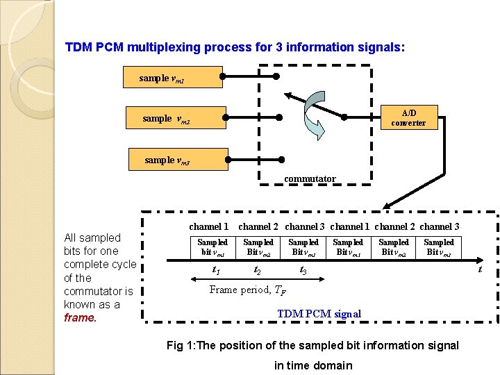
TDM PCM multiplexing process for 3 information signals: sample vm 1 A/D converter sample vm 2 sample vm 3 commutator All sampled bits for one complete cycle of the commutator is known as a frame. channel 1 channel 2 channel 3 channel 1 channel 2 channel 3 Sampled bit vm 1 Sampled Bit vm 2 Sampled Bit vm 3 t 1 t 2 t 3 Sampled Bit vm 1 Sampled Bit vm 2 Sampled Bit vm 3 Frame period, TF TDM PCM signal Fig 1: The position of the sampled bit information signal in time domain t

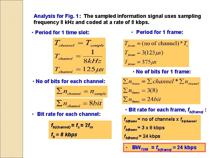
Analysis for Fig. 1: The sampled information signal uses sampling frequency 8 k. Hz and coded at a rate of 8 kbps. • Period for 1 time slot: • Period for 1 frame: • No of bits for each channel: • Bit rate for each channel: fb(channel) = fs = 2 fm fb = 8 kbps • Bit rate for each frame, fb(frame) : fb(frame = no of channels x fb(channel fb(frame = 3 x 8 kbps fb(frame) = 24 kbps • BWTDM = fb(frame) = 24 kbps

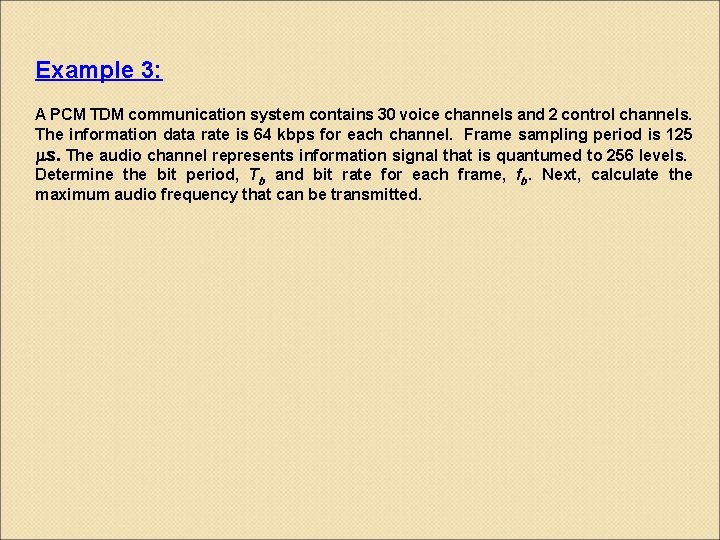
Example 3: A PCM TDM communication system contains 30 voice channels and 2 control channels. The information data rate is 64 kbps for each channel. Frame sampling period is 125 s. The audio channel represents information signal that is quantumed to 256 levels. Determine the bit period, Tb and bit rate for each frame, fb. Next, calculate the maximum audio frequency that can be transmitted.

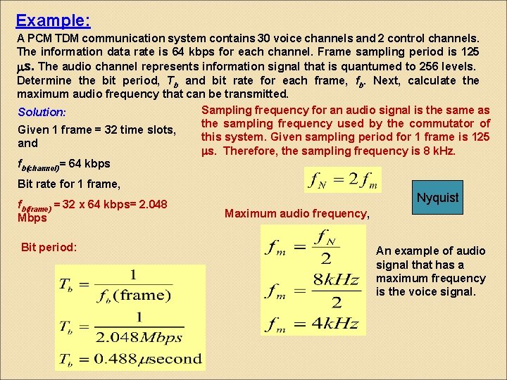
Example: A PCM TDM communication system contains 30 voice channels and 2 control channels. The information data rate is 64 kbps for each channel. Frame sampling period is 125 s. The audio channel represents information signal that is quantumed to 256 levels. Determine the bit period, Tb and bit rate for each frame, fb. Next, calculate the maximum audio frequency that can be transmitted. Sampling frequency for an audio signal is the same as Solution: the sampling frequency used by the commutator of Given 1 frame = 32 time slots, this system. Given sampling period for 1 frame is 125 and s. Therefore, the sampling frequency is 8 k. Hz. fb(channel)= 64 kbps Bit rate for 1 frame, fb(frame) = 32 x 64 kbps= 2. 048 Mbps Bit period: Nyquist Maximum audio frequency, An example of audio signal that has a maximum frequency is the voice signal.

THE END OF CHAPTER 6

THANK YOU