Chapter 1 Analysis versus design Analysis Given a


on")
")


 • Low-pressure chemical-vapor deposition • Plasma-assisted chemical-vapor deposition •")


 • p. MOS transistors in n-well • n. MOS")


 1. Cover the wafer with pad oxide and silicon nitride.")

- Slides: 63
Chapter 1
Analysis versus design • Analysis: – Given a system, find its properties. – The solution is unique. • Design: » Given a set of properties, come up with a system possessing them. » The solution is rarely unique.
Texas Instruments, or Vaibhav Kumar’s view
Electrical Design • the process from the specifications to a circuit solution • Requires active and passive device electrical models for – Creating the design – Verifying the design – Determining the robustness of the design
Physical Design • From electrical design to a layout pattern
Signal naming conventions
Appendix A
Circuit analysis skills • Please review materials in appendix A • Make sure you are fluent at – Nodal analysis, KCL – Mesh analysis (dual to nodal), KVL – Cascade stages – Small signal analysis, including linearization – Equivalent circuits, Thevenin, Norton – Miller simplification • Use google or wiki, if needed
Small signal analysis The amplifier may be nonlinear, but near an operating point, it has a small signal model of: vo = Av * vin. By definition, SSA is always linear.
Making Equivalent substitutions Simplified Cascade
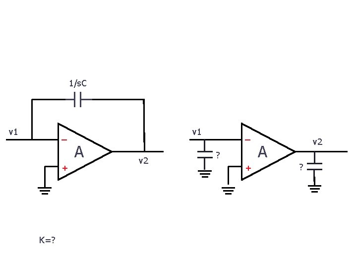
Miller simplification If v 2 = K*v 1 i 1 = (v 1 -Kv 1)/Z =(1 -K)v 1/Z i 2 = (v 2 -v 1/K)/Z =(K-1)/K v 2/Z
Chapter 2
BASIC FABRTICATION PROCESSES – Oxide growth – Thermal diffusion – Ion implantation – Deposition – Etching – Shallow trench isolation – Epitaxy • Photolithography • CMP
Oxidation • The process of growing a layer of silicon dioxide (Si. O 2)on the surface of a silicon wafer. • Uses: ü Provide isolation between two layers ü Protect underlying material from contamination ü Very thin oxides (100 to 1000 Å) are grown using dry-oxidation techniques. ü Thicker oxides (>1000 Å) are grown using wet oxidation techniques.
(Thickness of Si. O 2 grossly exaggerated. )
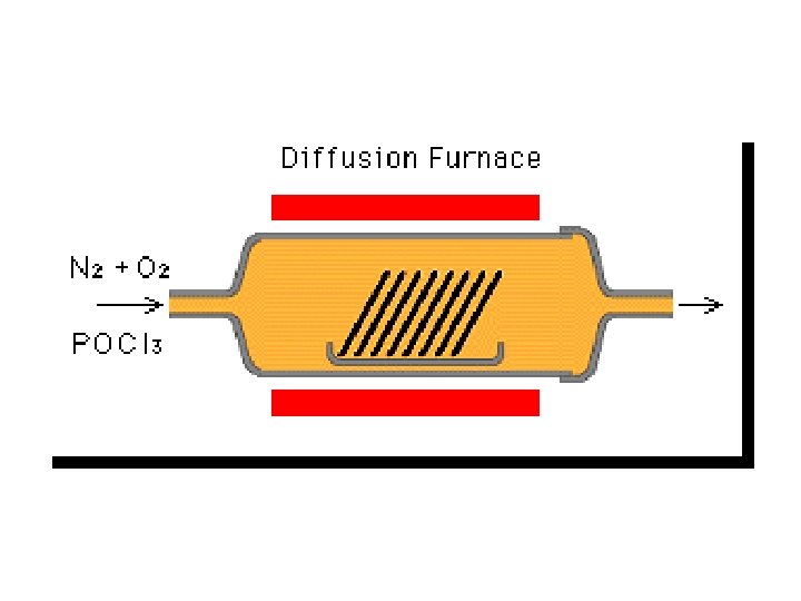
Diffusion Movement of impurity atoms at the surface of the silicon into the bulk of the silicon - From higher concentration to lower concentration. - Done at high temperatures: 800 to 1400 °C.
Infinite-source diffusion
Finite-source diffusion
Ion Implantation The process by which impurity ions are accelerated to a high velocity and physically lodged into the target.
• Require annealing to repair damage • Can implant through surface layers • Can achieve unique doping profile
Deposition • Chemical-vapor deposition (CVD) • Low-pressure chemical-vapor deposition • Plasma-assisted chemical-vapor deposition • Sputter deposition • Materials deposited – Silicon nitride (Si 3 N 4) – Silicon dioxide (Si. O 2) – Aluminum – Polysilicon
Etching • To selectively remove a layer of material • But may remove portions or all of – The desired material – The underlying layer – The masking layer • Two basic types of etches: – Wet etch, uses chemicals – Dry etch, uses chemically active ionized gasses.
etching Wet Etching
• Selectivity: • Anisotropy: a and b due to finite S c is due to non-unity A
Epitaxy • Epitaxial growth consists of the formation of a layer of single-crystal silicon on the surface of the silicon material so that the crystal structure of the silicon is continuous across the interfaces. – It is done externally to the material as opposed to diffusion which is internal – The epitaxial layer (epi) can be doped differently, even opposite to the material on which it is grown – It is accomplished at high temperatures using a chemical reaction at the surface – The epi layer can be any thickness, typically 1 -20 microns
Photolithography • Components – Photoresist material – Photomask – Material to be patterned (e. g. , Si. O 2) • Positive photoresist– Areas exposed to UV light are soluble in the developer • Negative photoresist– Areas not exposed to UV light are soluble in the developer
Steps: 1. Apply photoresist 2. Soft bake 3. Expose the photoresist to UV light through photomask 4. Develop (remove unwanted photoresist) 5. Hard bake 6. Etch the exposed layer 7. Remove photoresist
Expose: The process of exposing selective areas to light through a photo-mask is called printing. Types of printing include: • Contact printing • Proximity printing • Projection printing
After Developing
After Etching
After Removing Photoresist
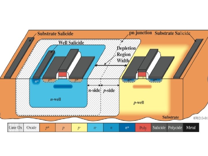
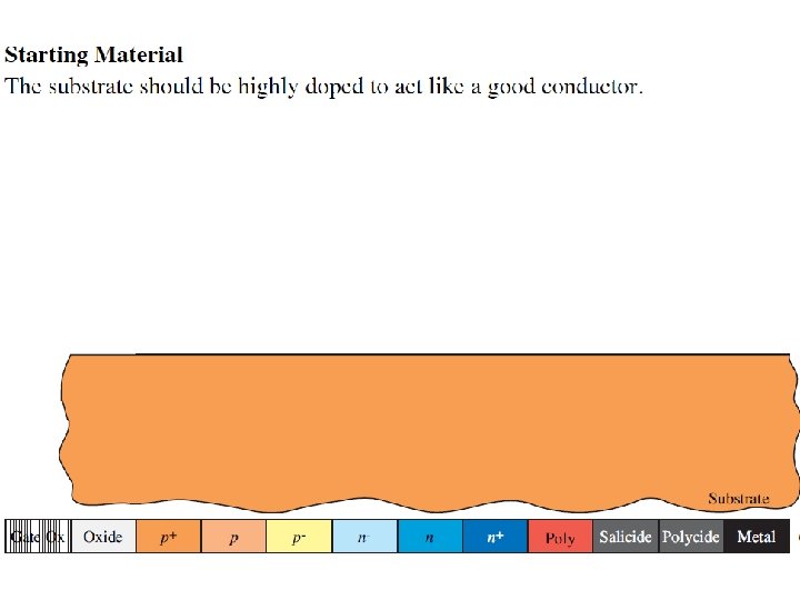
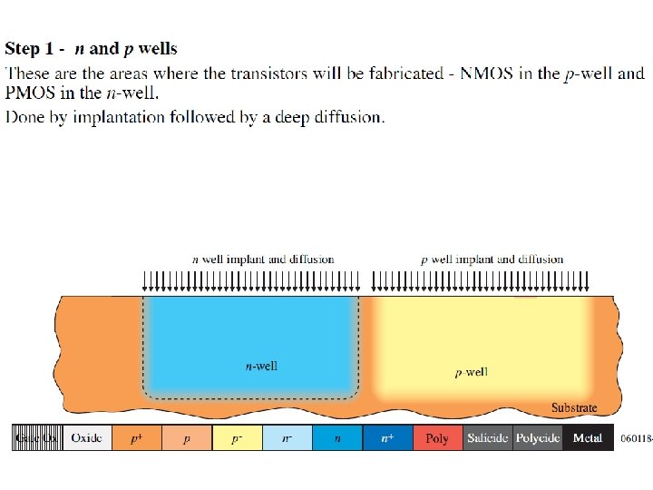
CMOS Technology • Flow varies with process types & company – N-Well CMOS (EE 330, 435, overview below) – Twin-Well CMOS (overview in 2. 1) – STI (for deep submicron, overview below) • Start with substrate selection – Type: n or p – Doping level, →resistivity – Orientation, 100, or 101, etc – Other parameters
N-well CMOS (ON. 5 um) • p. MOS transistors in n-well • n. MOS transistors on substrate • n. MOS transistor’s body is always connected to lowest voltage of chip – n. MOS is a three terminal device • p. MOS body can be tied to voltages other than Vdd – p. MOS is a four terminal device • 0. 35 um and larger typically n-well
VDD M 2 Vin Vo M 1
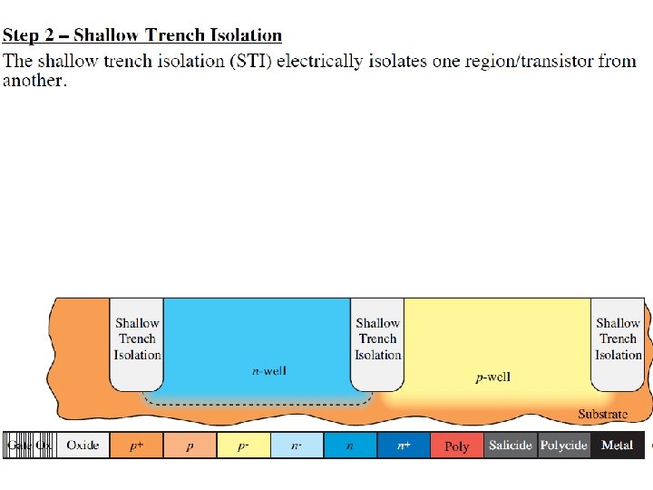
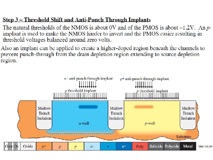
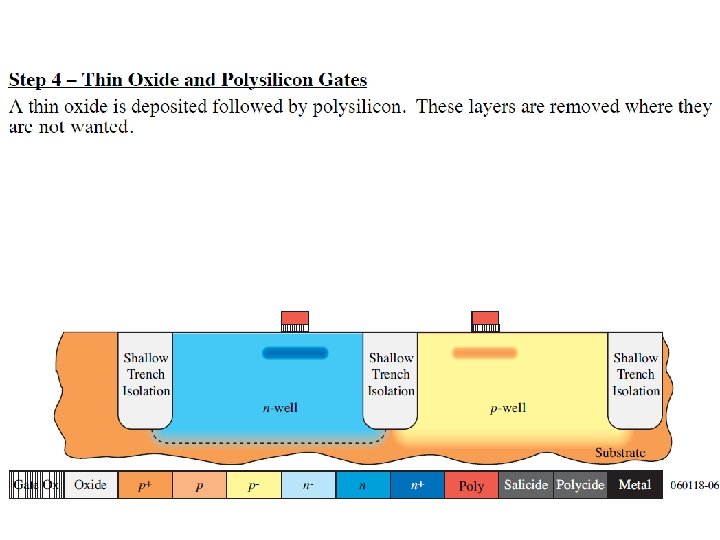
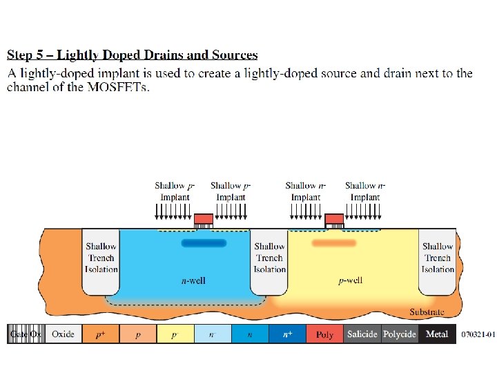
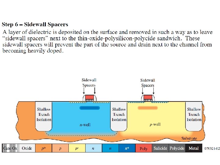
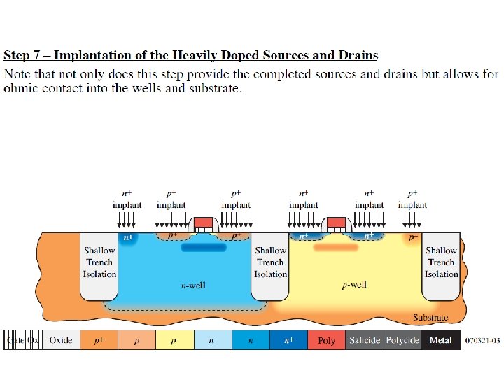
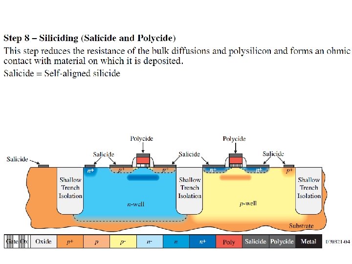
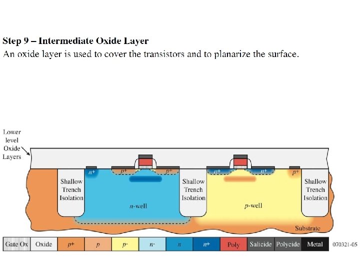
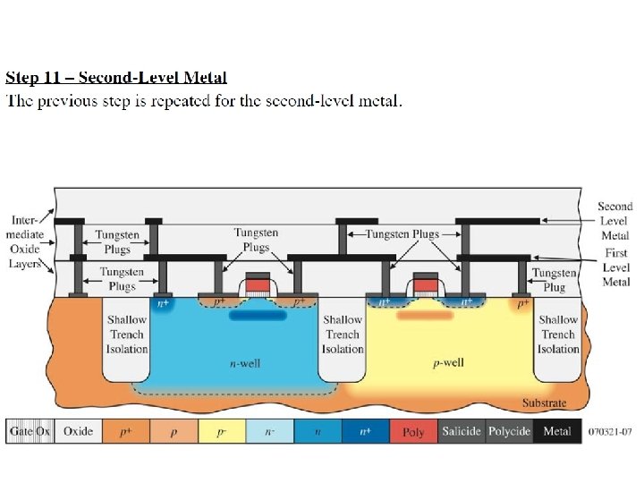
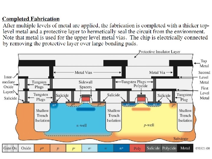
Major n-well CMOS Steps
Major n-well CMOS Steps
Major n-well CMOS Steps
Major n-well CMOS Steps
Major n-well CMOS Steps
Major n-well CMOS Steps
Major n-well CMOS Steps
Major n-well CMOS Steps
Relative size of different layers
• For twin well process step for the same inverter, refer to the book.
Deep Sub. Micron Challenges • Transistor sizes become very small • But FOX lateral size cannot be reduced • Depletion region between p-well and nwell not reduced • Large area FOX depletion
Shallow Trench Isolation Technology • Allowing transistors to be spaced closer
Shallow Trench Isolation (STI) 1. Cover the wafer with pad oxide and silicon nitride. 2. First etch nitride and pad oxide. Next, an anisotropic etch is made in the silicon to a depth of 0. 4 to 0. 5 microns. 3. Grow a thin thermal oxide layer on the trench walls. 4. A CVD dielectric film is used to fill the trench. 5. A chemical mechanical polishing (CMP) step is used to polish back the dielectric layer until the nitride is reached. The nitride acts like a CMP stop layer. 6. Densify the dielectric material at 900°C and strip the nitride and pad oxide.