Chap 5 Fieldeffect transistors FET Widely used in
![Transconductance = gm = d. ID/d. VGS = d [K(VGS-VT)2]/d. VGS = 2 K(VGS-VT) Transconductance = gm = d. ID/d. VGS = d [K(VGS-VT)2]/d. VGS = 2 K(VGS-VT)](https://slidetodoc.com/presentation_image/521ce1e89ec2ebd61e14b17c4bcc5ddc/image-20.jpg)
- Slides: 35

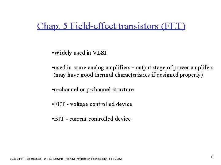
Chap. 5 Field-effect transistors (FET) • Widely used in VLSI • used in some analog amplifiers - output stage of power amplifers (may have good thermal characteristics if designed properly) • n-channel or p-channel structure • FET - voltage controlled device • BJT - current controlled device ECE 3111 - Electronics - Dr. S. Kozaitis- Florida Institute of Technology - Fall 2002 0

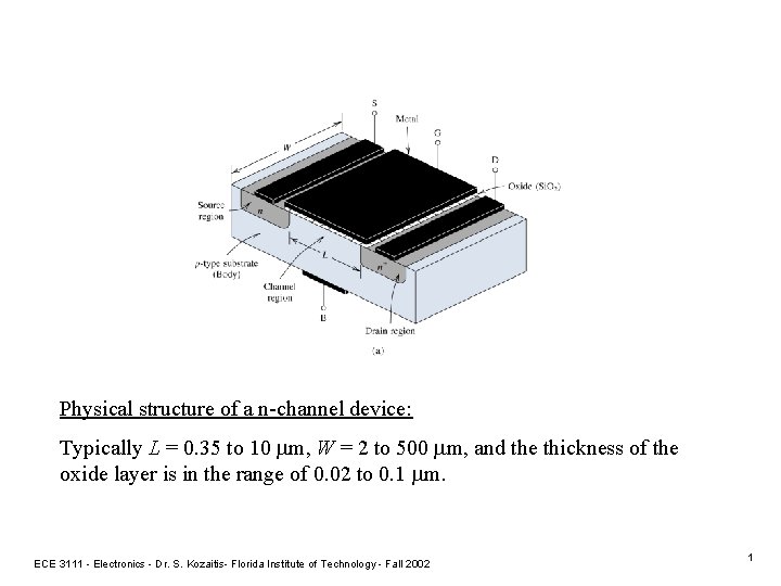
Physical structure of a n-channel device: Typically L = 0. 35 to 10 m, W = 2 to 500 m, and the thickness of the oxide layer is in the range of 0. 02 to 0. 1 m. ECE 3111 - Electronics - Dr. S. Kozaitis- Florida Institute of Technology - Fall 2002 1

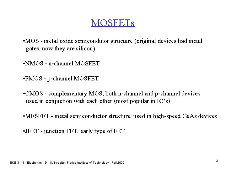
MOSFETs • MOS - metal oxide semicondutor structure (original devices had metal gates, now they are silicon) • NMOS - n-channel MOSFET • PMOS - p-channel MOSFET • CMOS - complementary MOS, both n-channel and p-channel devices used in conjuction with each other (most popular in IC’s) • MESFET - metal semiconductor structure, used in high-speed Ga. As devices • JFET - junction FET, early type of FET ECE 3111 - Electronics - Dr. S. Kozaitis- Florida Institute of Technology - Fall 2002 2

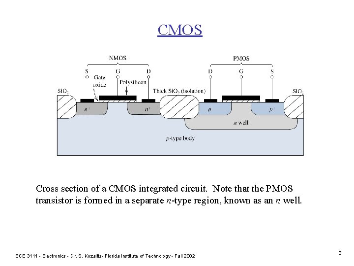
CMOS Cross section of a CMOS integrated circuit. Note that the PMOS transistor is formed in a separate n-type region, known as an n well. ECE 3111 - Electronics - Dr. S. Kozaitis- Florida Institute of Technology - Fall 2002 3

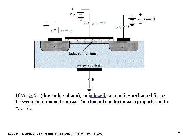
If VGS > VT (threshold voltage), an induced, conducting n-channel forms between the drain and source. The channel conductance is proportional to v. GS - Vt. ECE 3111 - Electronics - Dr. S. Kozaitis- Florida Institute of Technology - Fall 2002 4

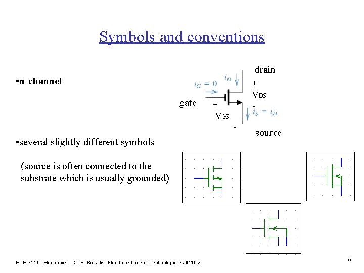
Symbols and conventions drain • n-channel gate + VDS - + VGS - • several slightly different symbols source (source is often connected to the substrate which is usually grounded) ECE 3111 - Electronics - Dr. S. Kozaitis- Florida Institute of Technology - Fall 2002 5

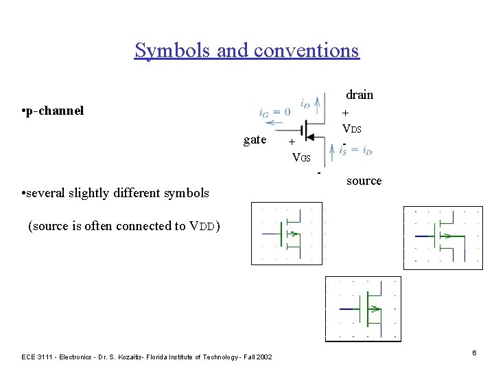
Symbols and conventions drain • p-channel gate + VDS - + VGS - • several slightly different symbols source (source is often connected to VDD) ECE 3111 - Electronics - Dr. S. Kozaitis- Florida Institute of Technology - Fall 2002 6

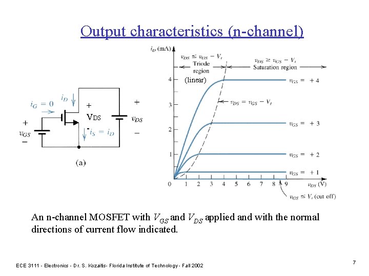
Output characteristics (n-channel) (linear) + VDS - An n-channel MOSFET with VGS and VDS applied and with the normal directions of current flow indicated. ECE 3111 - Electronics - Dr. S. Kozaitis- Florida Institute of Technology - Fall 2002 7

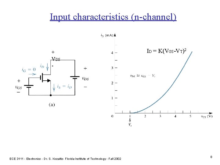
Input characteristics (n-channel) + VDS - ECE 3111 - Electronics - Dr. S. Kozaitis- Florida Institute of Technology - Fall 2002 ID = K(VGS-VT)2 8

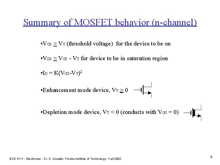
Summary of MOSFET behavior (n-channel) • VGS > VT (threshold voltage) for the device to be on • VDS > VGS - VT for device to be in saturation region • ID = K(VGS-VT)2 • Enhancement mode device, VT > 0 • Depletion mode device, VT < 0 (conducts with VGS = 0) ECE 3111 - Electronics - Dr. S. Kozaitis- Florida Institute of Technology - Fall 2002 9

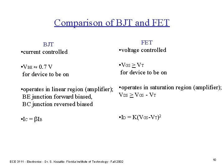
Comparison of BJT and FET BJT • current controlled FET • voltage controlled • VBE 0. 7 V for device to be on • VGS > VT for device to be on • operates in linear region (amplifier); • operates in saturation region (amplifier); VDS > VGS - VT BE junction forward biased, BC junction reversed biased • IC = b. IB • ID = K(VGS-VT)2 ECE 3111 - Electronics - Dr. S. Kozaitis- Florida Institute of Technology - Fall 2002 10

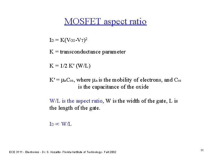
MOSFET aspect ratio ID = K(VGS-VT)2 K = transconductance parameter K = 1/2 K' (W/L) K' = n. Cox, where n is the mobility of electrons, and Cox is the capacitance of the oxide W/L is the aspect ratio, W is the width of the gate, L is the length of the gate. ID W/L ECE 3111 - Electronics - Dr. S. Kozaitis- Florida Institute of Technology - Fall 2002 11

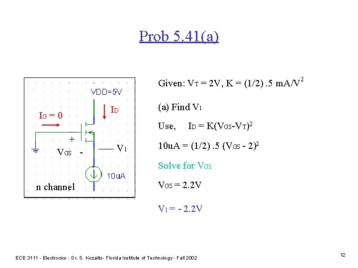
Prob 5. 41(a) Given: VT = 2 V, K = (1/2). 5 m. A/V 2 ID IG = 0 (a) Find V 1 Use, + VGS - V 1 ID = K(VGS-VT)2 10 u. A = (1/2). 5 (VGS - 2)2 Solve for VGS n channel VGS = 2. 2 V V 1 = - 2. 2 V ECE 3111 - Electronics - Dr. S. Kozaitis- Florida Institute of Technology - Fall 2002 12

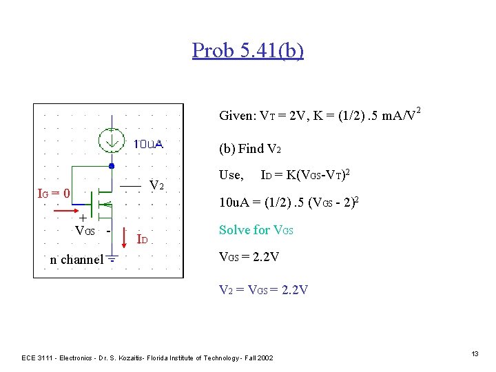
Prob 5. 41(b) Given: VT = 2 V, K = (1/2). 5 m. A/V 2 (b) Find V 2 IG = 0 Use, ID = K(VGS-VT)2 10 u. A = (1/2). 5 (VGS - 2)2 + VGS - n channel ID Solve for VGS = 2. 2 V V 2 = VGS = 2. 2 V ECE 3111 - Electronics - Dr. S. Kozaitis- Florida Institute of Technology - Fall 2002 13

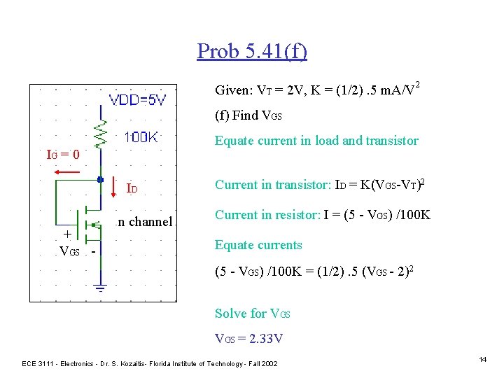
Prob 5. 41(f) Given: VT = 2 V, K = (1/2). 5 m. A/V 2 (f) Find VGS Equate current in load and transistor IG = 0 ID + VGS - n channel Current in transistor: ID = K(VGS-VT)2 Current in resistor: I = (5 - VGS) /100 K Equate currents (5 - VGS) /100 K = (1/2). 5 (VGS - 2)2 Solve for VGS = 2. 33 V ECE 3111 - Electronics - Dr. S. Kozaitis- Florida Institute of Technology - Fall 2002 14

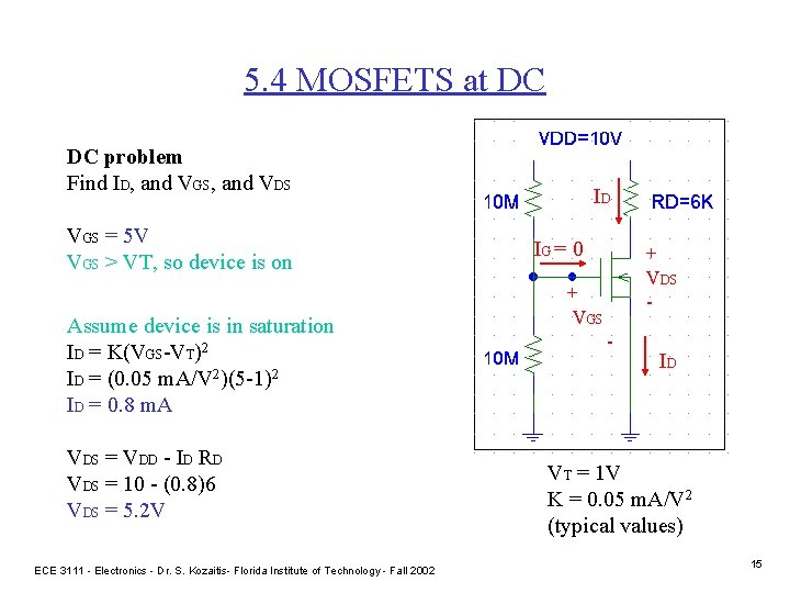
5. 4 MOSFETS at DC DC problem Find ID, and VGS, and VDS VGS = 5 V VGS > VT, so device is on Assume device is in saturation ID = K(VGS-VT)2 ID = (0. 05 m. A/V 2)(5 -1)2 ID = 0. 8 m. A VDS = VDD - ID RD VDS = 10 - (0. 8)6 VDS = 5. 2 V ECE 3111 - Electronics - Dr. S. Kozaitis- Florida Institute of Technology - Fall 2002 ID IG = 0 + VDS - + VGS - ID VT = 1 V K = 0. 05 m. A/V 2 (typical values) 15

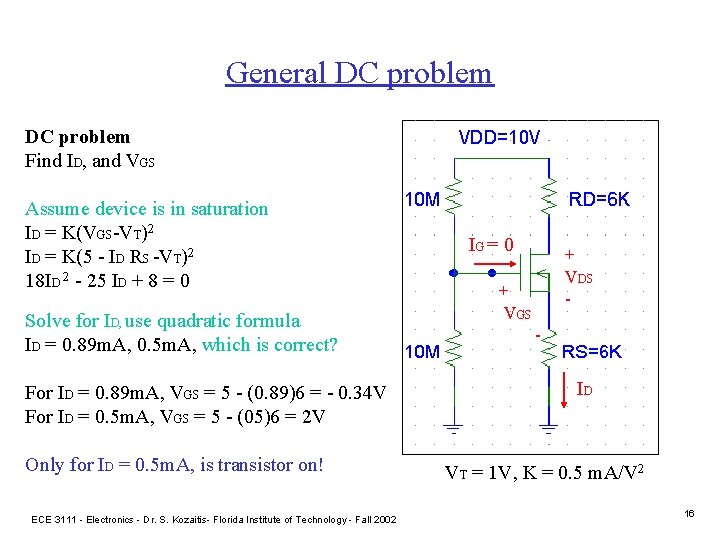
General DC problem Find ID, and VGS Assume device is in saturation ID = K(VGS-VT)2 ID = K(5 - ID RS -VT)2 18 ID 2 - 25 ID + 8 = 0 Solve for ID, use quadratic formula ID = 0. 89 m. A, 0. 5 m. A, which is correct? For ID = 0. 89 m. A, VGS = 5 - (0. 89)6 = - 0. 34 V For ID = 0. 5 m. A, VGS = 5 - (05)6 = 2 V Only for ID = 0. 5 m. A, is transistor on! ECE 3111 - Electronics - Dr. S. Kozaitis- Florida Institute of Technology - Fall 2002 IG = 0 + VDS - + VGS - ID VT = 1 V, K = 0. 5 m. A/V 2 16

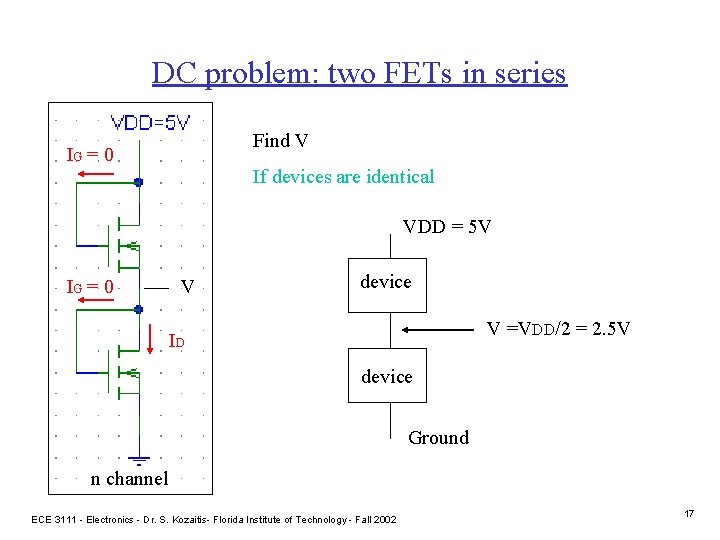
DC problem: two FETs in series Find V IG = 0 If devices are identical VDD = 5 V IG = 0 V device V =VDD/2 = 2. 5 V ID device Ground n channel ECE 3111 - Electronics - Dr. S. Kozaitis- Florida Institute of Technology - Fall 2002 17

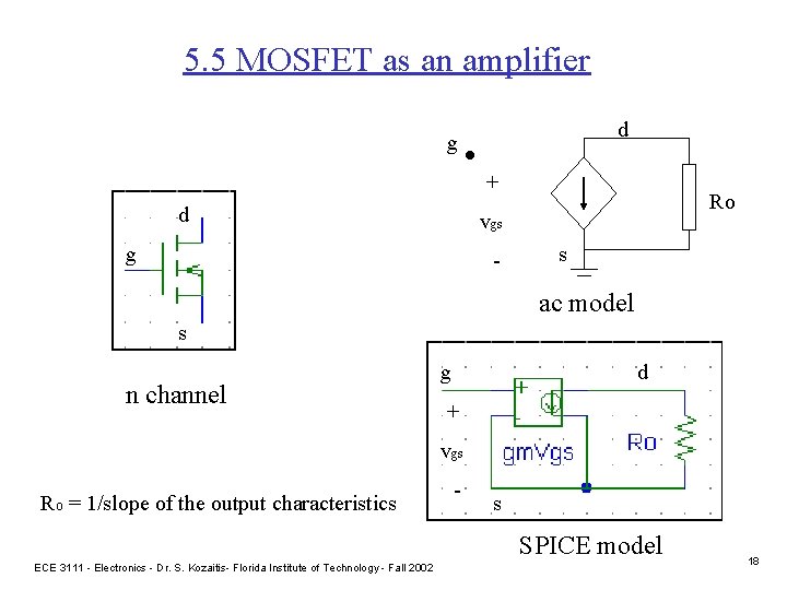
5. 5 MOSFET as an amplifier g . d d + Ro vgs g - s ac model s n channel g d + vgs Ro = 1/slope of the output characteristics - s SPICE model ECE 3111 - Electronics - Dr. S. Kozaitis- Florida Institute of Technology - Fall 2002 18
![Transconductance gm d IDd VGS d KVGSVT2d VGS 2 KVGSVT Transconductance = gm = d. ID/d. VGS = d [K(VGS-VT)2]/d. VGS = 2 K(VGS-VT)](https://slidetodoc.com/presentation_image/521ce1e89ec2ebd61e14b17c4bcc5ddc/image-20.jpg)
Transconductance = gm = d. ID/d. VGS = d [K(VGS-VT)2]/d. VGS = 2 K(VGS-VT) Useful relation: gm = 2 K ID ECE 3111 - Electronics - Dr. S. Kozaitis- Florida Institute of Technology - Fall 2002 19

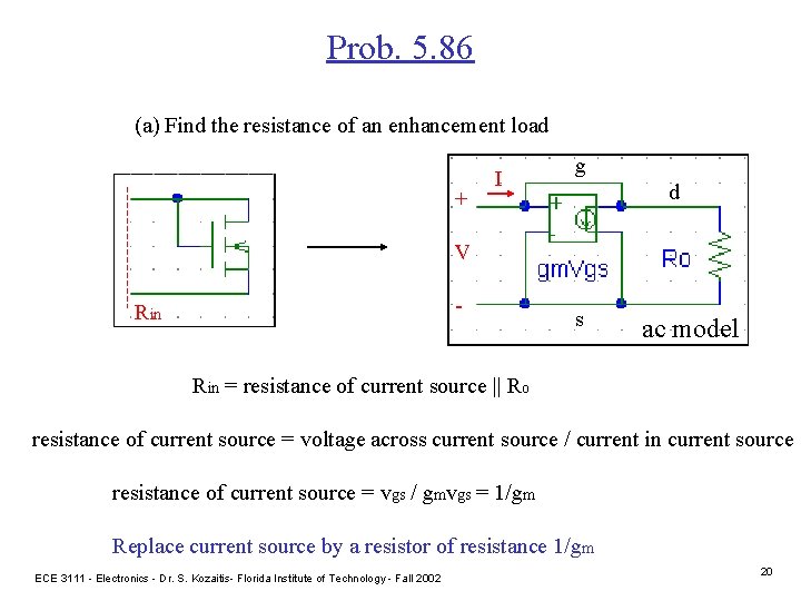
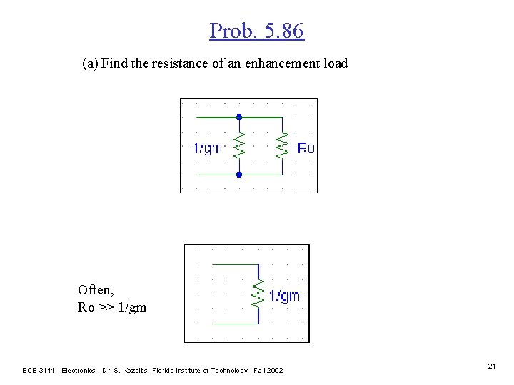
Prob. 5. 86 (a) Find the resistance of an enhancement load + I g d V - Rin s ac model Rin = resistance of current source || Ro resistance of current source = voltage across current source / current in current source resistance of current source = vgs / gmvgs = 1/gm Replace current source by a resistor of resistance 1/gm ECE 3111 - Electronics - Dr. S. Kozaitis- Florida Institute of Technology - Fall 2002 20

Prob. 5. 86 (a) Find the resistance of an enhancement load Often, Ro >> 1/gm ECE 3111 - Electronics - Dr. S. Kozaitis- Florida Institute of Technology - Fall 2002 21

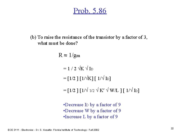
Prob. 5. 86 (b) To raise the resistance of the transistor by a factor of 3, what must be done? R 1/gm = 1 / 2 K ID = [1/2 ] [1/ K] [ 1/ ID] = [1/2 ] [1/ 1/2 K W/L ] [ 1/ ID] • Decrease ID by a factor of 9 • Decrease W by a factor of 9 • Increase L by a factor of 9 ECE 3111 - Electronics - Dr. S. Kozaitis- Florida Institute of Technology - Fall 2002 22

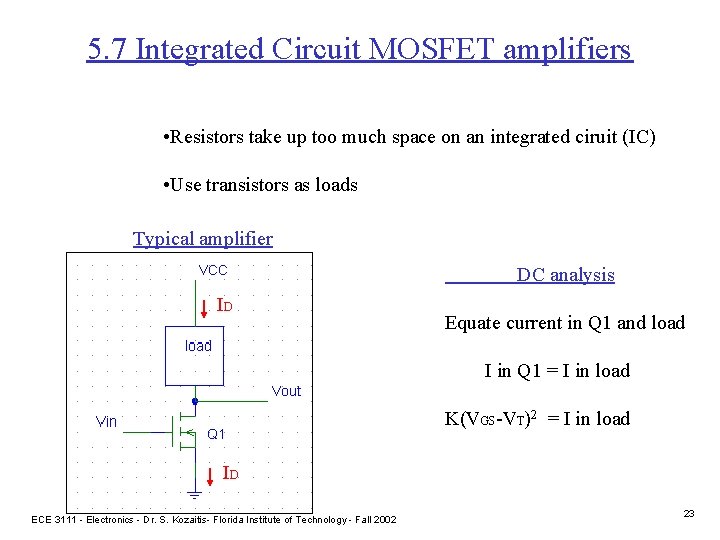
5. 7 Integrated Circuit MOSFET amplifiers • Resistors take up too much space on an integrated ciruit (IC) • Use transistors as loads Typical amplifier DC analysis ID Equate current in Q 1 and load I in Q 1 = I in load K(VGS-VT)2 = I in load ID ECE 3111 - Electronics - Dr. S. Kozaitis- Florida Institute of Technology - Fall 2002 23

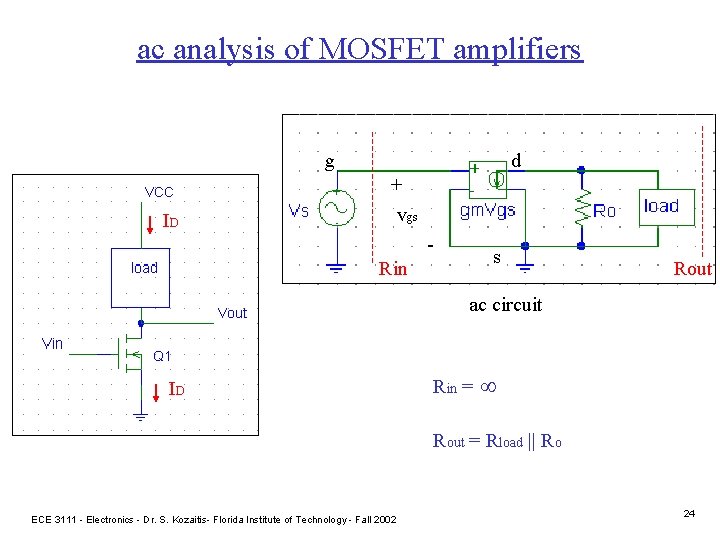
ac analysis of MOSFET amplifiers g ID d + vgs - s Rin Rout ac circuit ID Rin = Rout = Rload || Ro ECE 3111 - Electronics - Dr. S. Kozaitis- Florida Institute of Technology - Fall 2002 24

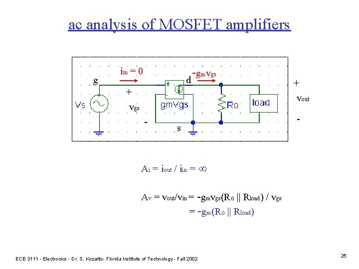
ac analysis of MOSFET amplifiers g iin = 0 d -gmvgs + vgs - - s Ai = iout / iin = + vout Av = vout/vin = -gmvgs(Ro || Rload) / vgs = -gm(Ro || Rload) ECE 3111 - Electronics - Dr. S. Kozaitis- Florida Institute of Technology - Fall 2002 25

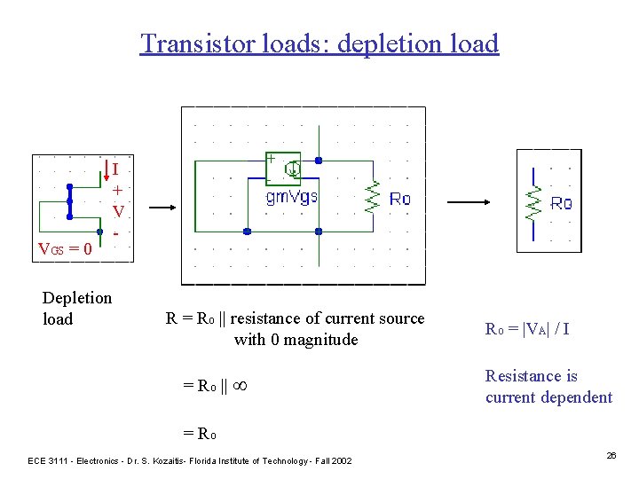
Transistor loads: depletion load VGS = 0 Depletion load I + V - R = Ro || resistance of current source with 0 magnitude = Ro || Ro = |VA| / I Resistance is current dependent = Ro ECE 3111 - Electronics - Dr. S. Kozaitis- Florida Institute of Technology - Fall 2002 26

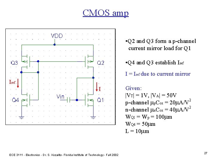
CMOS amp • Q 2 and Q 3 form a p-channel current mirror load for Q 1 • Q 4 and Q 3 establish Iref I = Iref due to current mirror Iref I ECE 3111 - Electronics - Dr. S. Kozaitis- Florida Institute of Technology - Fall 2002 Given: |VT| = 1 V, |VA| = 50 V p-channel p. Cox = 20 A/V 2 n-channel n. Cox = 40 A/V 2 WQ 1 = Wp = 100 m WQ 4 = 50 m L = 10 m 27

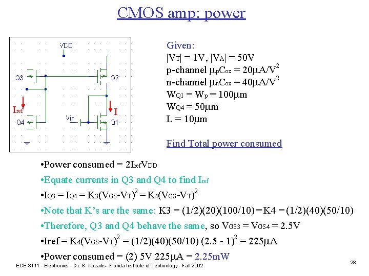
CMOS amp: power Iref I Given: |VT| = 1 V, |VA| = 50 V p-channel p. Cox = 20 A/V 2 n-channel n. Cox = 40 A/V 2 WQ 1 = Wp = 100 m WQ 4 = 50 m L = 10 m Find Total power consumed • Power consumed = 2 Iref. VDD • Equate currents in Q 3 and Q 4 to find Iref • IQ 3 = IQ 4 = K 3(VGS-VT)2 = K 4(VGS-VT)2 • Note that K’s are the same: K 3 = (1/2)(20)(100/10) = K 4 = (1/2)(40)(50/10) • Therefore, Q 3 and Q 4 behave the same, so VGS 3 = VGS 4 = 2. 5 V • Iref = K 4(VGS-VT)2 = (1/2)(40)(50/10) (2. 5 - 1)2 = 225 A • Power consumed = (2) 5 V 225 A = 2. 25 m. W 28 ECE 3111 - Electronics - Dr. S. Kozaitis- Florida Institute of Technology - Fall 2002

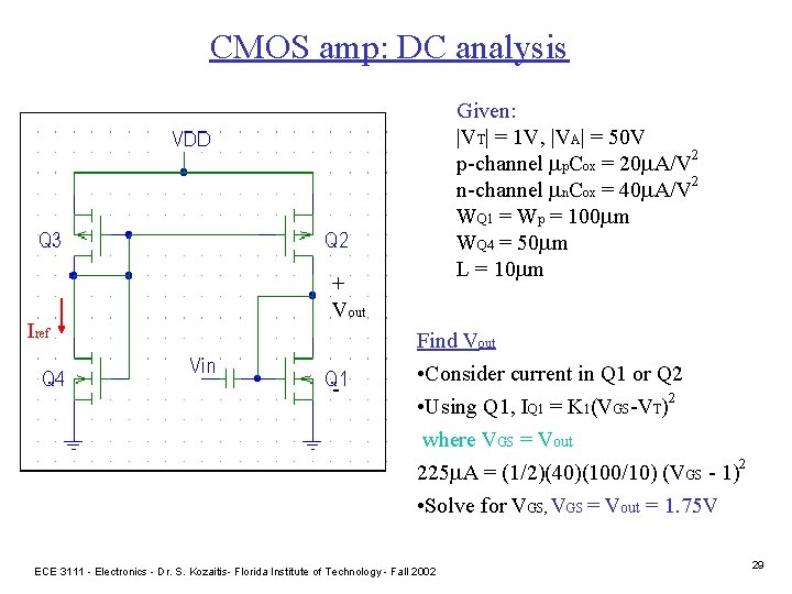
CMOS amp: DC analysis Iref Given: |VT| = 1 V, |VA| = 50 V p-channel p. Cox = 20 A/V 2 n-channel n. Cox = 40 A/V 2 WQ 1 = Wp = 100 m WQ 4 = 50 m L = 10 m + Vout - Find Vout • Consider current in Q 1 or Q 2 • Using Q 1, IQ 1 = K 1(VGS-VT)2 where VGS = Vout 225 A = (1/2)(40)(100/10) (VGS - 1)2 • Solve for VGS, VGS = Vout = 1. 75 V ECE 3111 - Electronics - Dr. S. Kozaitis- Florida Institute of Technology - Fall 2002 29

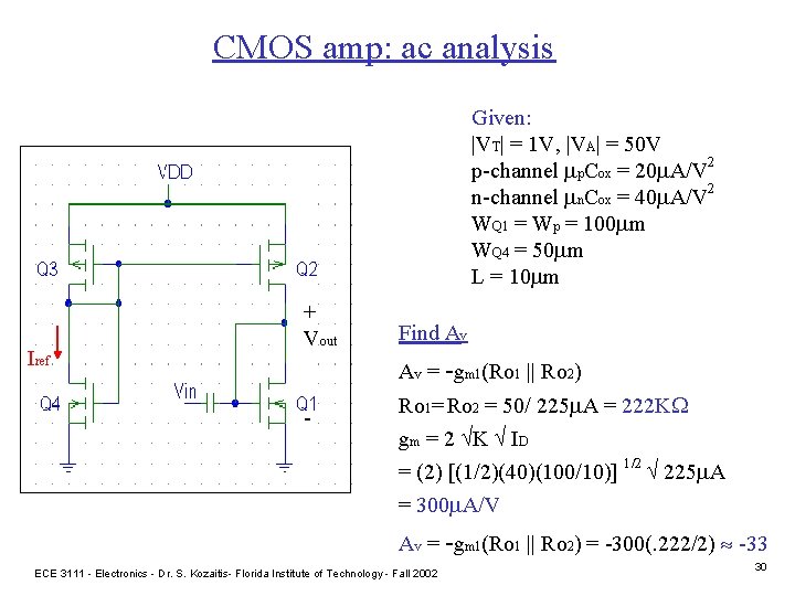
CMOS amp: ac analysis Given: |VT| = 1 V, |VA| = 50 V p-channel p. Cox = 20 A/V 2 n-channel n. Cox = 40 A/V 2 WQ 1 = Wp = 100 m WQ 4 = 50 m L = 10 m Iref + Vout Find Av Av = -gm 1(Ro 1 || Ro 2) - Ro 1= Ro 2 = 50/ 225 A = 222 KW gm = 2 K ID = (2) [(1/2)(40)(100/10)] 1/2 225 A = 300 A/V Av = -gm 1(Ro 1 || Ro 2) = -300(. 222/2) -33 ECE 3111 - Electronics - Dr. S. Kozaitis- Florida Institute of Technology - Fall 2002 30

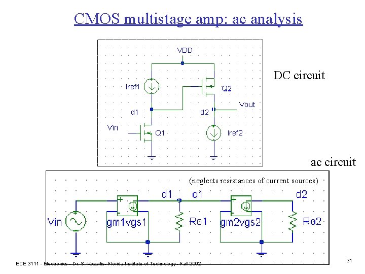
CMOS multistage amp: ac analysis DC circuit ac circuit (neglects resistances of current sources) ECE 3111 - Electronics - Dr. S. Kozaitis- Florida Institute of Technology - Fall 2002 31

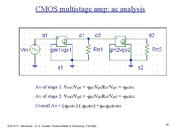
CMOS multistage amp: ac analysis Av of stage 1: Vout 1/Vgs 1 = -gm 1 Vgs 1 Ro 1/Vgs 1 = -gm 1 ro 1 Av of stage 2: Vout 2/Vgs 2 = -gm 2 Vgs 2 Ro 2/Vgs 2 = -gm 2 ro 2 Overall Av = (-gm 1 ro 1) ( -gm 2 ro 2) = gm 1 gm 2 ro 1 ro 2 ECE 3111 - Electronics - Dr. S. Kozaitis- Florida Institute of Technology - Fall 2002 32

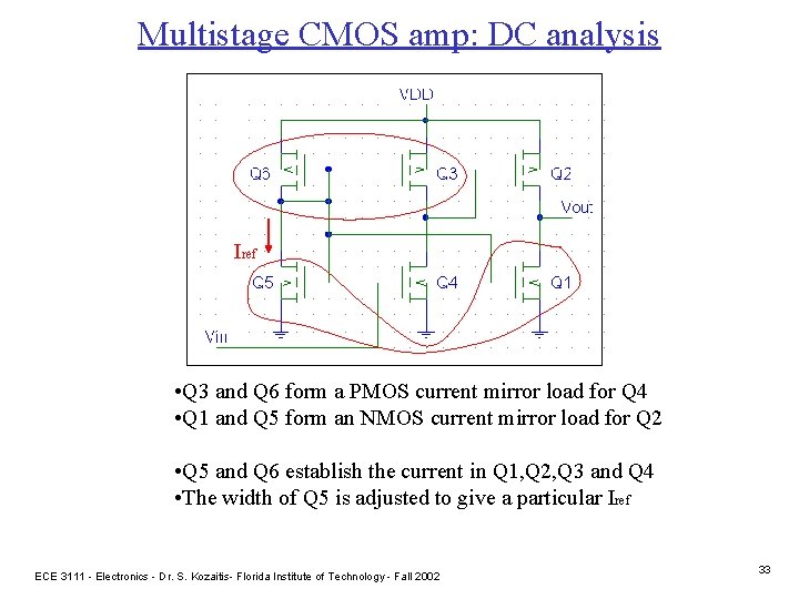
Multistage CMOS amp: DC analysis Iref • Q 3 and Q 6 form a PMOS current mirror load for Q 4 • Q 1 and Q 5 form an NMOS current mirror load for Q 2 • Q 5 and Q 6 establish the current in Q 1, Q 2, Q 3 and Q 4 • The width of Q 5 is adjusted to give a particular Iref ECE 3111 - Electronics - Dr. S. Kozaitis- Florida Institute of Technology - Fall 2002 33

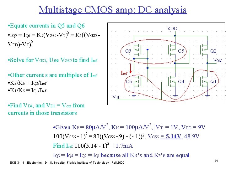
Multistage CMOS amp: DC analysis • Equate currents in Q 5 and Q 6 • IQ 5 = IQ 6 = K 5(VGS 5 -VT)2 = K 6((VGS 5 VDD)-VT)2 • Solve for VGS 5, Use VGS 5 to find Iref • Other current s are multiples of Iref • K 3/K 6 = IQ 3/Iref • K 1/K 5 = IQ 1/Iref • Find VD 4, and VD 1 = Vout from currents in those transistors • Given KP = 80 A/V 2, KN = 100 A/V 2, |VT| = 1 V, VDD = 9 V 100(VGS 5 - 1)2 = 80((VGS 5 - 9) - (- 1))2, VGS 5 = 5. 14 V, 48. 9 V Find Iref, 100(5. 14 - 1)2 = 1. 7 m. A IQ 3 = IQ 4 = IQ 2 = IQ 1 because all KN’s and KP’s are equal ECE 3111 - Electronics - Dr. S. Kozaitis- Florida Institute of Technology - Fall 2002 34