FieldEffect Transistors Chapter 20 Introduction An Overview of
- Slides: 32

Field-Effect Transistors Chapter 20 § Introduction § An Overview of Field-Effect Transistors § Insulated-Gate Field-Effect Transistors § Junction-Gate Field-Effect Transistors § FET Characteristics § Summary of FET Characteristics § FET Amplifiers § Other FET Applications Storey: Electrical & Electronic Systems © Pearson Education Limited 2004 OHT 20. 1

Introduction 20. 1 § Field-effect transistors (FETs) are probably the simplest form of transistor – widely used in both analogue and digital applications – they are characterised by a very high input resistance and small physical size, and they can be used to form circuits with a low power consumption – they are widely used in very large-scale integration – two basic forms: § insulated gate FETs § junction gate FETs Storey: Electrical & Electronic Systems © Pearson Education Limited 2004 OHT 20. 2

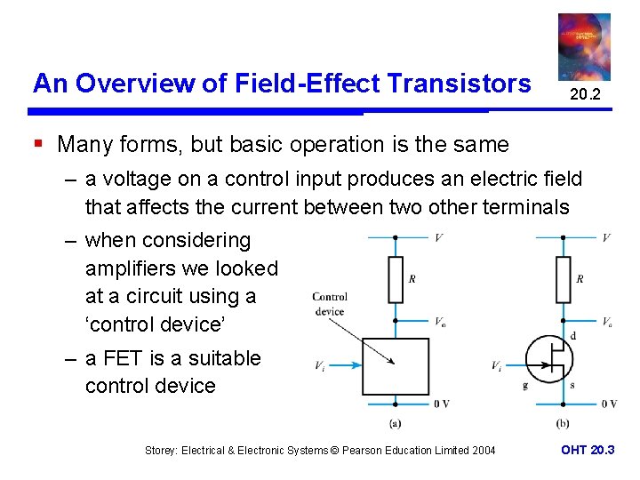
An Overview of Field-Effect Transistors 20. 2 § Many forms, but basic operation is the same – a voltage on a control input produces an electric field that affects the current between two other terminals – when considering amplifiers we looked at a circuit using a ‘control device’ – a FET is a suitable control device Storey: Electrical & Electronic Systems © Pearson Education Limited 2004 OHT 20. 3

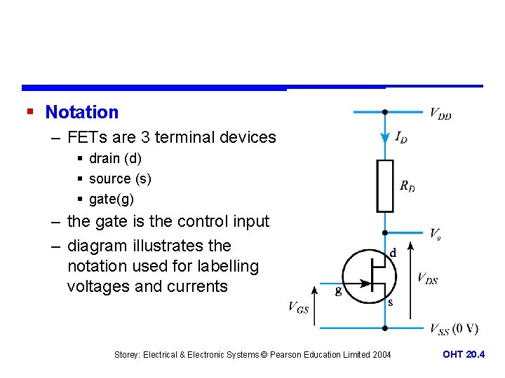
§ Notation – FETs are 3 terminal devices § drain (d) § source (s) § gate(g) – the gate is the control input – diagram illustrates the notation used for labelling voltages and currents Storey: Electrical & Electronic Systems © Pearson Education Limited 2004 OHT 20. 4

Insulated-Gate Field-Effect Transistors 20. 3 § Such devices are sometimes called IGFETs (insulated-gate field-effect transistors) or sometimes MOSFETs (metal oxide semiconductor field-effect transistors) § Digital circuits constructed using these devices are usually described as using MOS technology § Here we will describe them as MOSFETs Storey: Electrical & Electronic Systems © Pearson Education Limited 2004 OHT 20. 5

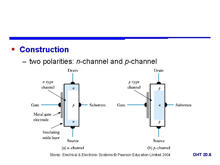
§ Construction – two polarities: n-channel and p-channel Storey: Electrical & Electronic Systems © Pearson Education Limited 2004 OHT 20. 6

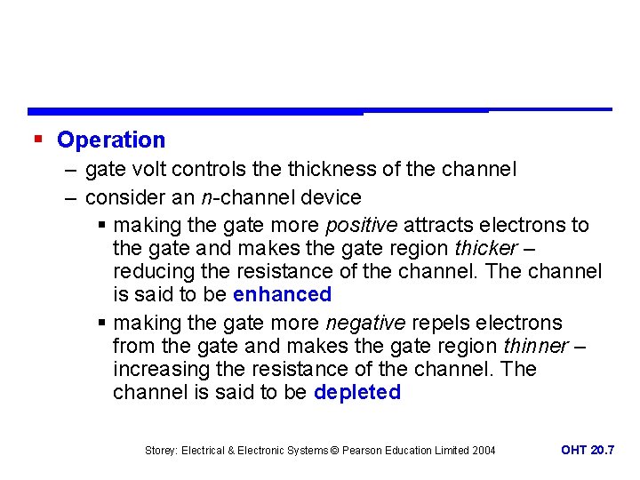
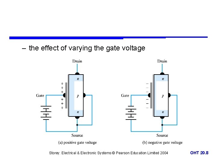
§ Operation – gate volt controls the thickness of the channel – consider an n-channel device § making the gate more positive attracts electrons to the gate and makes the gate region thicker – reducing the resistance of the channel. The channel is said to be enhanced § making the gate more negative repels electrons from the gate and makes the gate region thinner – increasing the resistance of the channel. The channel is said to be depleted Storey: Electrical & Electronic Systems © Pearson Education Limited 2004 OHT 20. 7

– the effect of varying the gate voltage Storey: Electrical & Electronic Systems © Pearson Education Limited 2004 OHT 20. 8

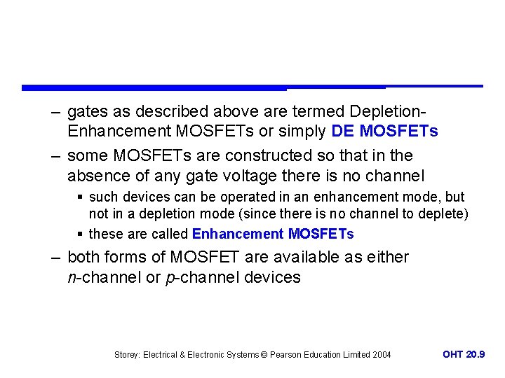
– gates as described above are termed Depletion. Enhancement MOSFETs or simply DE MOSFETs – some MOSFETs are constructed so that in the absence of any gate voltage there is no channel § such devices can be operated in an enhancement mode, but not in a depletion mode (since there is no channel to deplete) § these are called Enhancement MOSFETs – both forms of MOSFET are available as either n-channel or p-channel devices Storey: Electrical & Electronic Systems © Pearson Education Limited 2004 OHT 20. 9

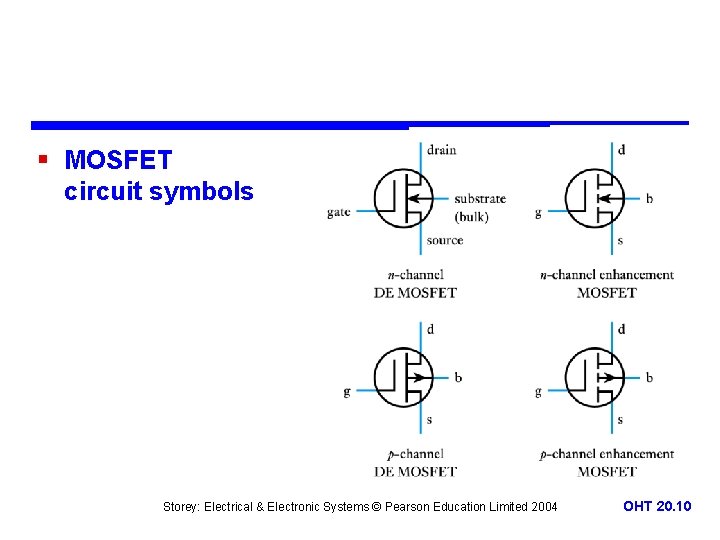
§ MOSFET circuit symbols Storey: Electrical & Electronic Systems © Pearson Education Limited 2004 OHT 20. 10

Junction-Gate Field-Effect Transistors 20. 4 § Sometimes known as a JUGFET § Here we will use another common name – the JFET § Here the insulated gate of a MOSFET is replaced with a reverse-biased pn junction § Since the gate junction is always reverse-biased no current flows into the gate and it acts as if it were insulated Storey: Electrical & Electronic Systems © Pearson Education Limited 2004 OHT 20. 11

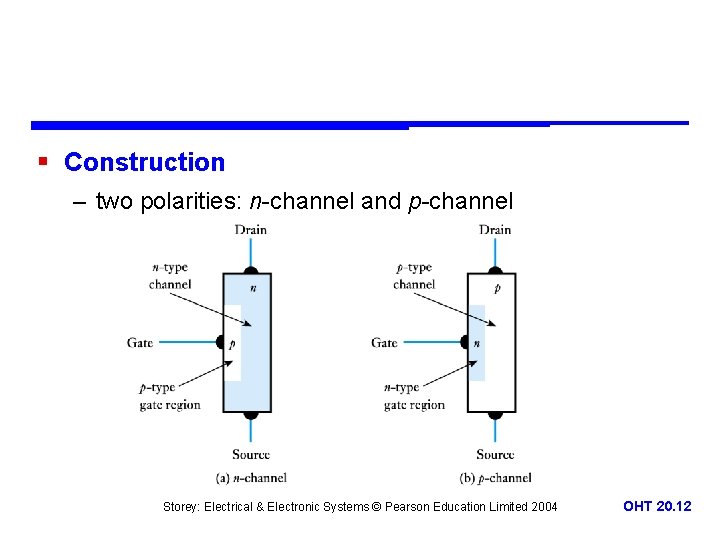
§ Construction – two polarities: n-channel and p-channel Storey: Electrical & Electronic Systems © Pearson Education Limited 2004 OHT 20. 12

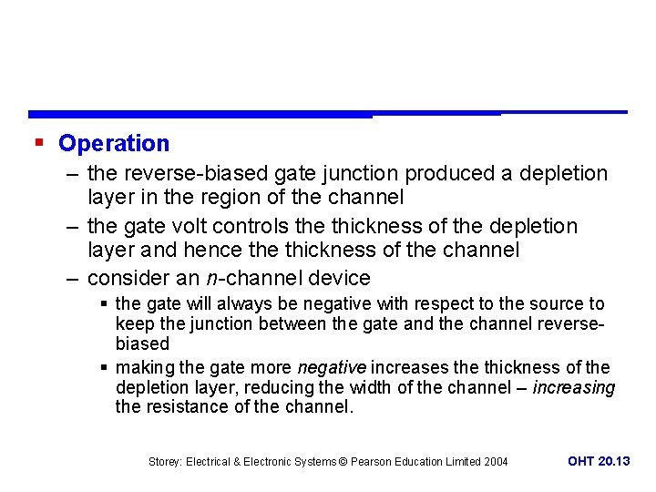
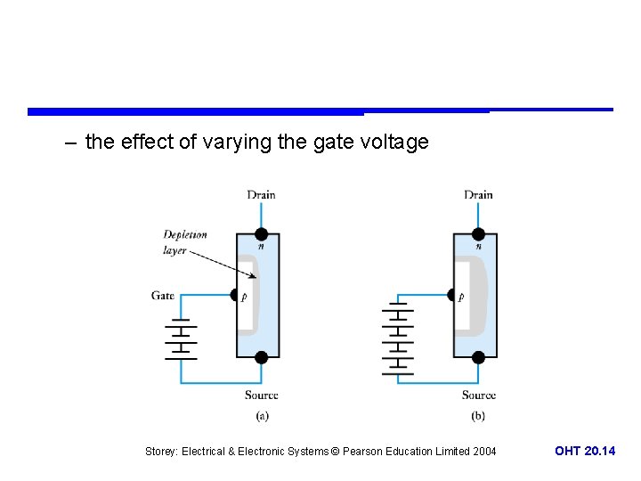
§ Operation – the reverse-biased gate junction produced a depletion layer in the region of the channel – the gate volt controls the thickness of the depletion layer and hence thickness of the channel – consider an n-channel device § the gate will always be negative with respect to the source to keep the junction between the gate and the channel reversebiased § making the gate more negative increases the thickness of the depletion layer, reducing the width of the channel – increasing the resistance of the channel. Storey: Electrical & Electronic Systems © Pearson Education Limited 2004 OHT 20. 13

– the effect of varying the gate voltage Storey: Electrical & Electronic Systems © Pearson Education Limited 2004 OHT 20. 14

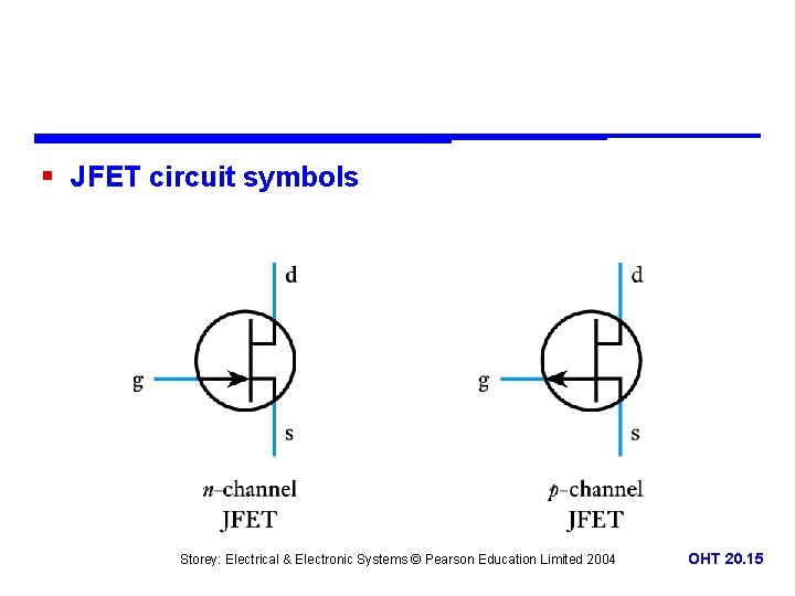
§ JFET circuit symbols Storey: Electrical & Electronic Systems © Pearson Education Limited 2004 OHT 20. 15

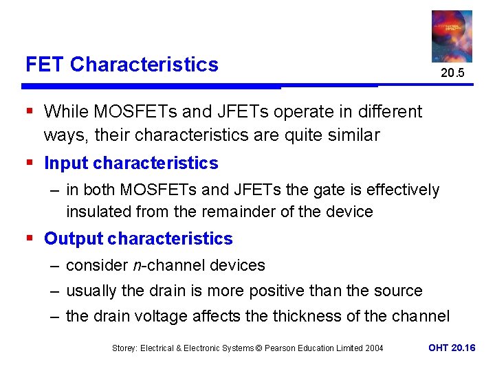
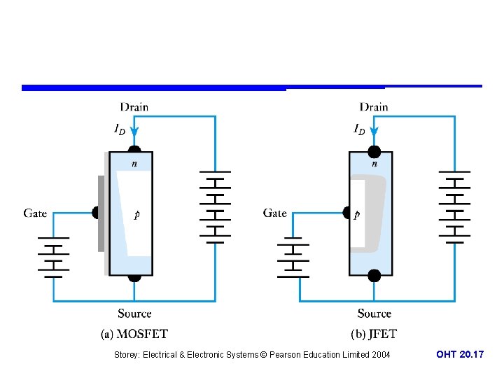
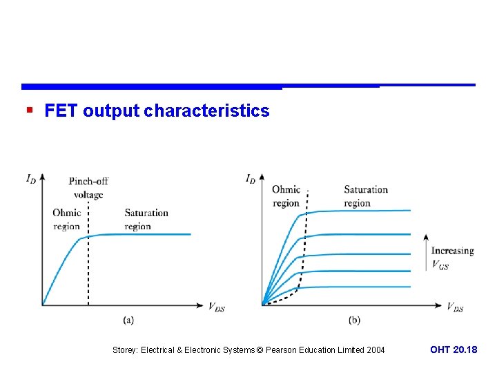
FET Characteristics 20. 5 § While MOSFETs and JFETs operate in different ways, their characteristics are quite similar § Input characteristics – in both MOSFETs and JFETs the gate is effectively insulated from the remainder of the device § Output characteristics – consider n-channel devices – usually the drain is more positive than the source – the drain voltage affects the thickness of the channel Storey: Electrical & Electronic Systems © Pearson Education Limited 2004 OHT 20. 16

Storey: Electrical & Electronic Systems © Pearson Education Limited 2004 OHT 20. 17

§ FET output characteristics Storey: Electrical & Electronic Systems © Pearson Education Limited 2004 OHT 20. 18

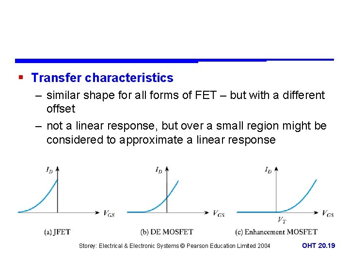
§ Transfer characteristics – similar shape for all forms of FET – but with a different offset – not a linear response, but over a small region might be considered to approximate a linear response Storey: Electrical & Electronic Systems © Pearson Education Limited 2004 OHT 20. 19

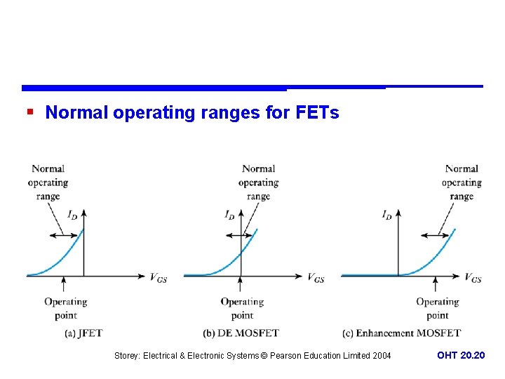
§ Normal operating ranges for FETs Storey: Electrical & Electronic Systems © Pearson Education Limited 2004 OHT 20. 20

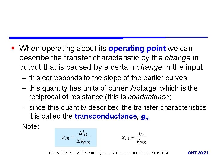
§ When operating about its operating point we can describe the transfer characteristic by the change in output that is caused by a certain change in the input – this corresponds to the slope of the earlier curves – this quantity has units of current/voltage, which is the reciprocal of resistance (this is conductance) – since this quantity described the transfer characteristics it is called the transconductance, gm Note: Storey: Electrical & Electronic Systems © Pearson Education Limited 2004 OHT 20. 21

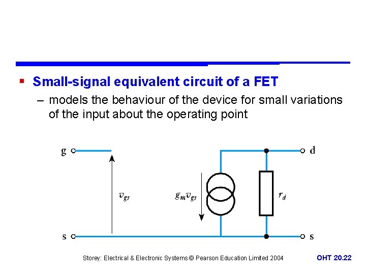
§ Small-signal equivalent circuit of a FET – models the behaviour of the device for small variations of the input about the operating point Storey: Electrical & Electronic Systems © Pearson Education Limited 2004 OHT 20. 22

Summary of FET Characteristics 20. 6 § FETS have three terminals: drain, source and gate § The gate is the control input § Two polarities of device: n-channel and p-channel § Two main forms of FET: MOSFET and JFET § In each case the drain current is controlled by the voltage applied to the gate with respect to the source § Behaviour is characterised by the transconductance § The operating point differs between devices Storey: Electrical & Electronic Systems © Pearson Education Limited 2004 OHT 20. 23

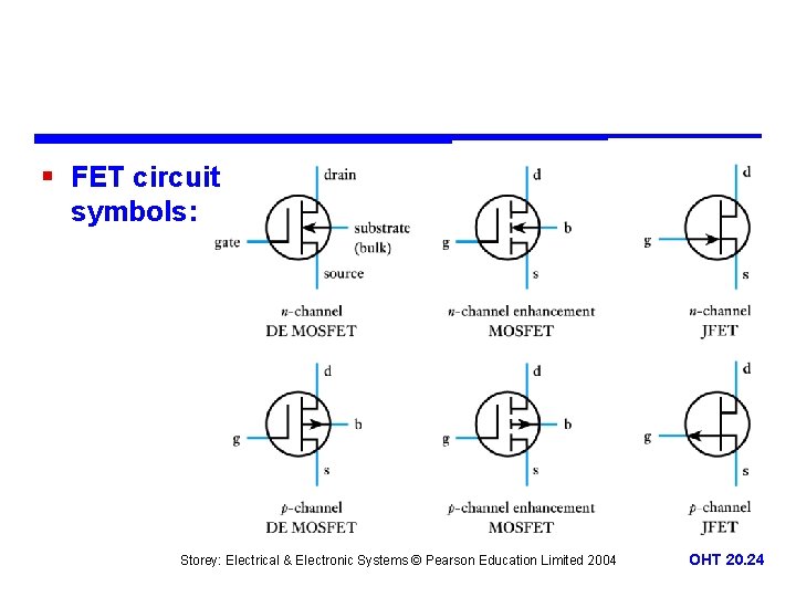
§ FET circuit symbols: Storey: Electrical & Electronic Systems © Pearson Education Limited 2004 OHT 20. 24

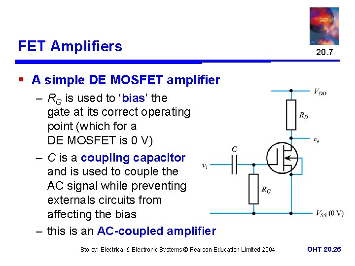
FET Amplifiers 20. 7 § A simple DE MOSFET amplifier – RG is used to ‘bias’ the gate at its correct operating point (which for a DE MOSFET is 0 V) – C is a coupling capacitor and is used to couple the AC signal while preventing externals circuits from affecting the bias – this is an AC-coupled amplifier Storey: Electrical & Electronic Systems © Pearson Education Limited 2004 OHT 20. 25

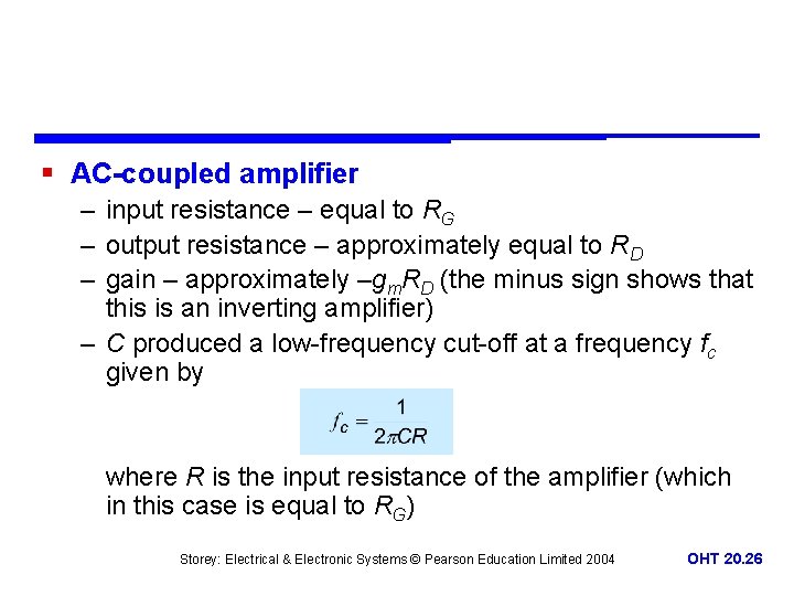
§ AC-coupled amplifier – input resistance – equal to RG – output resistance – approximately equal to RD – gain – approximately –gm. RD (the minus sign shows that this is an inverting amplifier) – C produced a low-frequency cut-off at a frequency fc given by where R is the input resistance of the amplifier (which in this case is equal to RG) Storey: Electrical & Electronic Systems © Pearson Education Limited 2004 OHT 20. 26

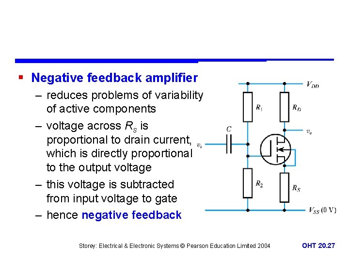
§ Negative feedback amplifier – reduces problems of variability of active components – voltage across Rs is proportional to drain current, which is directly proportional to the output voltage – this voltage is subtracted from input voltage to gate – hence negative feedback Storey: Electrical & Electronic Systems © Pearson Education Limited 2004 OHT 20. 27

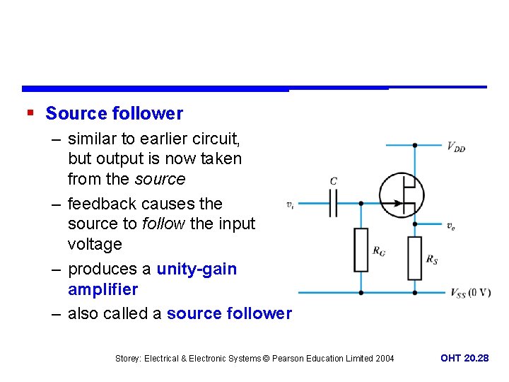
§ Source follower – similar to earlier circuit, but output is now taken from the source – feedback causes the source to follow the input voltage – produces a unity-gain amplifier – also called a source follower Storey: Electrical & Electronic Systems © Pearson Education Limited 2004 OHT 20. 28

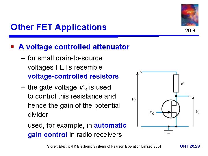
Other FET Applications 20. 8 § A voltage controlled attenuator – for small drain-to-source voltages FETs resemble voltage-controlled resistors – the gate voltage VG is used to control this resistance and hence the gain of the potential divider – used, for example, in automatic gain control in radio receivers Storey: Electrical & Electronic Systems © Pearson Education Limited 2004 OHT 20. 29

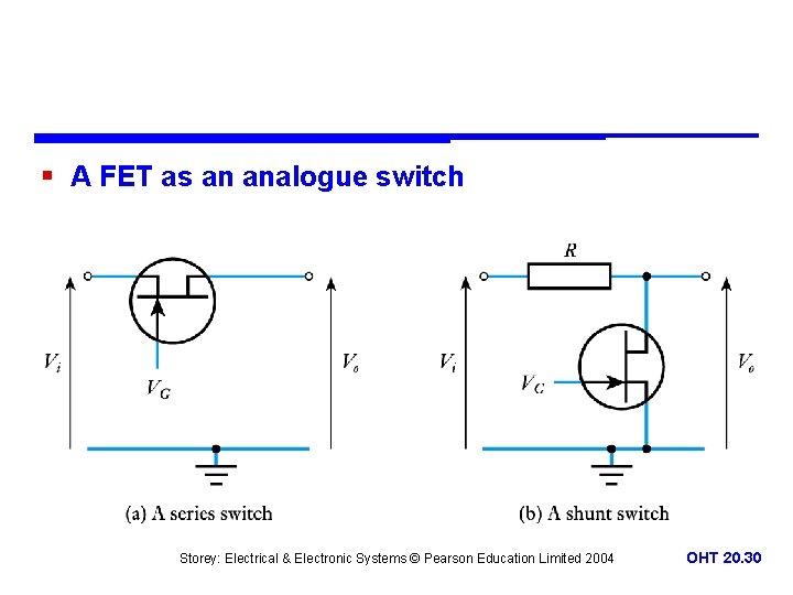
§ A FET as an analogue switch Storey: Electrical & Electronic Systems © Pearson Education Limited 2004 OHT 20. 30

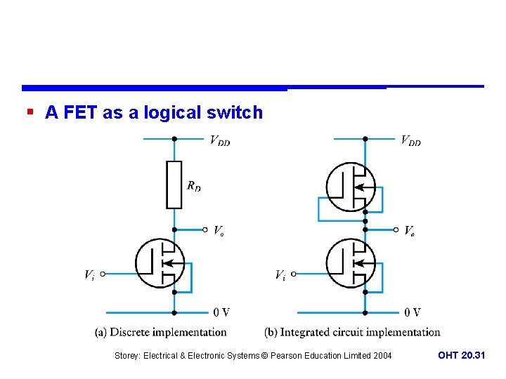
§ A FET as a logical switch Storey: Electrical & Electronic Systems © Pearson Education Limited 2004 OHT 20. 31

Key Points § § § FETs are widely used in both analogue and digital circuits They have high input resistance and small physical size There are two basic forms of FET: MOSFETs and JFETs MOSFETs may be divided into DE and Enhancement types In each case the gate voltage controls the current from the drain to the source § The characteristics of the various forms of FET are similar except that they require different bias voltages § The use of coupling capacitors prevents the amplification of DC and produced AC amplifiers § FETs can be used to produce various forms of amplifier and a range of other circuit applications Storey: Electrical & Electronic Systems © Pearson Education Limited 2004 OHT 20. 32