Application of superconducting Resonators for Study of Two
- Slides: 30

Application of superconducting Resonators for Study of Two Level Defect States in Dielectrics Sergiy Gladchenko Laboratory for Physical Sciences, Maryland Collaborators: Moe Khalil, Micah Stoutimore, K. D. Osborn (LPS) F. C. Wellstood, C. J. Lobb (UMD)

Outline: Common problems of superconducting quantum computing Two-level defect states in dielectric is a powerful source of decoherence in superconducting qubit Resonance methods of study of defect states in dielectric. Experimental observation of TLS-TLS interaction Resonance absorption of dielectric in the swept DC field

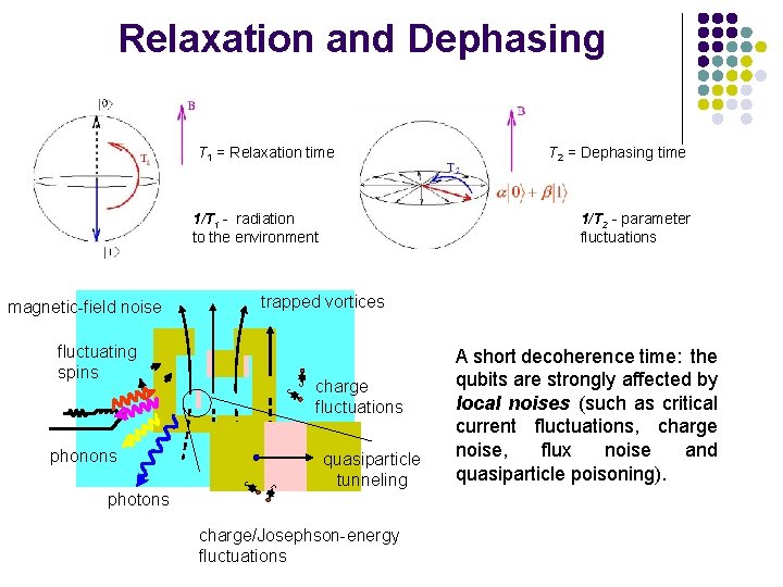
Relaxation and Dephasing T 1 = Relaxation time 1/T 1 - radiation to the environment magnetic-field noise fluctuating spins phonons T 2 = Dephasing time 1/T 2 - parameter fluctuations trapped vortices charge fluctuations quasiparticle tunneling photons charge/Josephson-energy fluctuations A short decoherence time: the qubits are strongly affected by local noises (such as critical current fluctuations, charge noise, flux noise and quasiparticle poisoning).

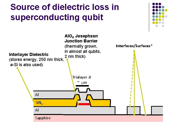
Source of dielectric loss in superconducting qubit Interlayer Dielectric (stores energy, 250 nm thick, a-Si is also used) Al. OX Josephson Junction Barrier (thermally grown, in almost all qubits, 2 nm thick) Trialayer JJ ~ m Al Si. NX Al Sapphire Interfaces/Surfaces*

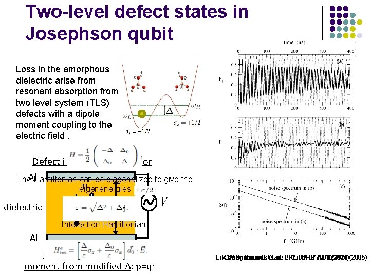
Two-level defect states in Josephson qubit Loss in the amorphous dielectric arise from resonant absorption from two level system (TLS) defects with a dipole moment coupling to the electric field. a b c d e f Defect in dielectric capacitor The. Al. Hamiltonian can be diagonalized to give the h eigenenergies dielectric Interaction Hamiltonian Al ac electric field: E=V/d moment from modified : p=qr Li-Chung R. W. Simmonds Ku and Clare et al. C. PRL Yu 93, PRB 077003 72, 024526 (2004) (2005)

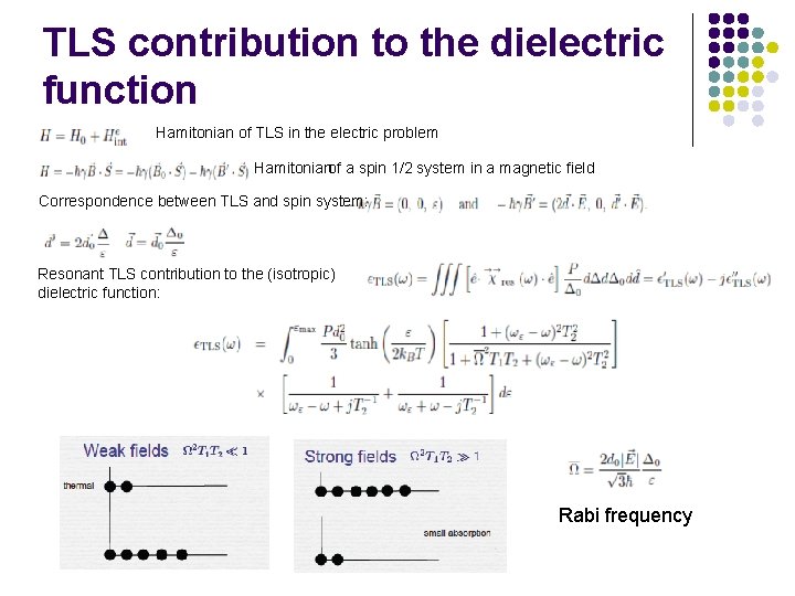
TLS contribution to the dielectric function Hamitonian of TLS in the electric problem Hamitonianof a spin 1/2 system in a magnetic field Correspondence between TLS and spin system: Resonant TLS contribution to the (isotropic) dielectric function: Rabi frequency

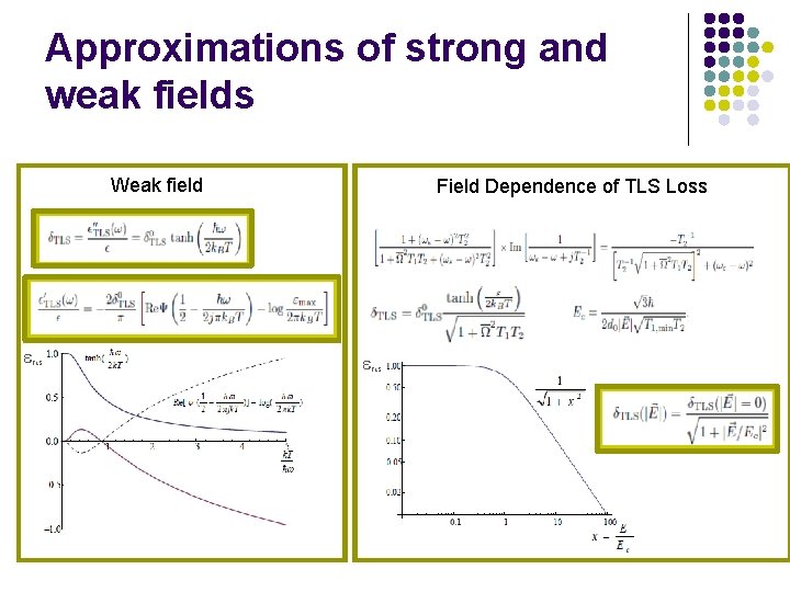
Approximations of strong and weak fields Weak field TLS We Field Dependence of TLS Loss TLS

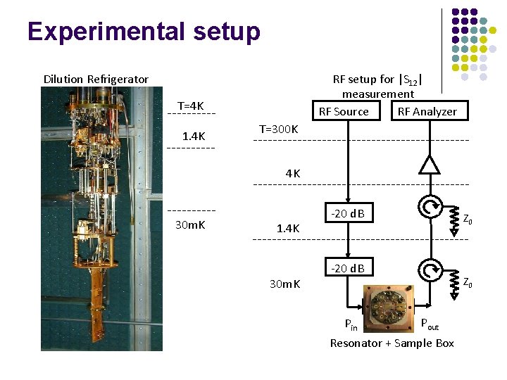
Experimental setup Dilution Refrigerator RF setup for |S 12| measurement RF Source RF Analyzer T=4 K 1. 4 K T=300 K 4 K 30 m. K 1. 4 K 30 m. K -20 d. B Z 0 -20 d. B Pin Z 0 Pout Resonator + Sample Box

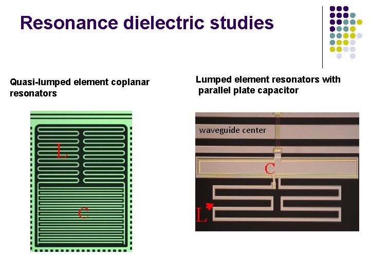
Resonance dielectric studies Quasi-lumped element coplanar resonators Lumped element resonators with parallel plate capacitor waveguide center L C C L

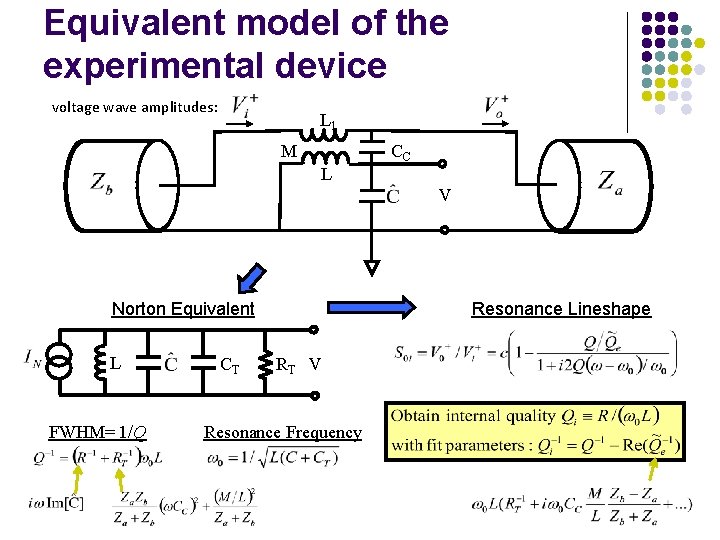
Equivalent model of the experimental device voltage wave amplitudes: L 1 M L CC V Norton Equivalent L FWHM= 1/Q CT Resonance Lineshape RT V Resonance Frequency

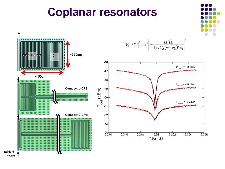
Coplanar resonators L C ~350 m ~450 m Compact L-CPS Compact C-CPS incident wave

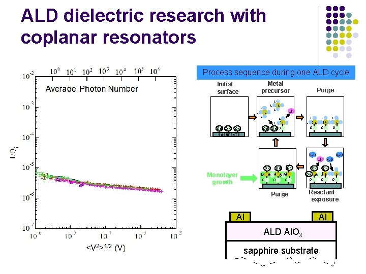
ALD dielectric research with coplanar resonators Process sequence during one ALD cycle Metal precursor exposure L Initial surface L LM L L LH L L M LL M L L LM L OH OH O OH Purge O O SUBSTRATE H 2 O OH Monolayer growth M O O OH M O Purge LH H 2 O OH L OH OH M O M L LM L O O O Reactant B exposure Al Al H 2 O ALD Al. Ox sapphire substrate

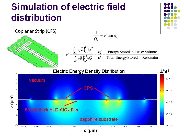
Simulation of electric field distribution Coplanar Strip (CPS) Electric Energy Density Distribution vacuum z (µm) CPS 50 nm thick ALD Al. Ox film sapphire substrate x (µm) J/m 3

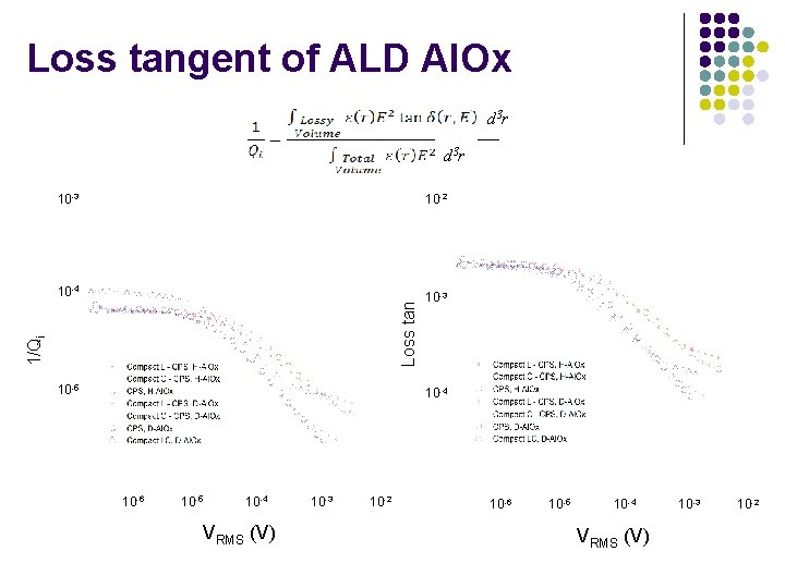
Loss tangent of ALD Al. Ox d 3 r 10 -2 10 -4 10 -3 1/Qi Loss tan 10 -3 10 -5 10 -4 10 -6 10 -5 10 -4 VRMS (V) 10 -3 10 -2

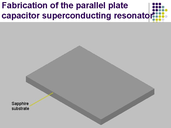
Fabrication of the parallel plate capacitor superconducting resonator Capacitor Al(200 nm) (bottom plate) Si. Nx (250 nm) Inductor Al (100 nm) Sapphire substrate Wave guide

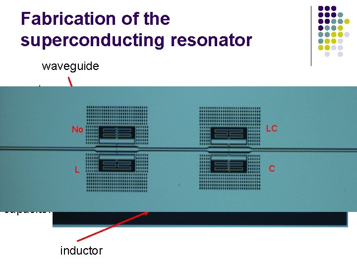
Fabrication of the superconducting resonator waveguide ground plane No LC L C 20 m capacitor inductor

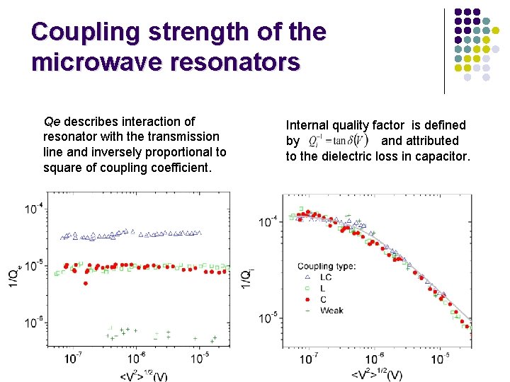
Coupling strength of the microwave resonators Qe describes interaction of resonator with the transmission line and inversely proportional to square of coupling coefficient. Internal quality factor is defined by and attributed to the dielectric loss in capacitor.

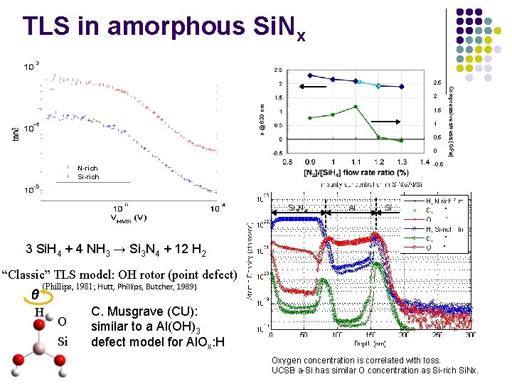
TLS in amorphous Si. Nx n @ 633 nm 2 1. 5 1 0. 5 0 Compressive stress (GPa) 2. 5 -0. 5 N-rich Si 3 N 4 Al Si 3 Si. H 4 + 4 NH 3 → Si 3 N 4 + 12 H 2 “Classic” TLS model: OH rotor (point defect) (Phillips, 1981; Hutt, Phillips, Butcher, 1989) θ H O Si C. Musgrave (CU): similar to a Al(OH)3 defect model for Al. Ox: H Oxygen concentration is correlated with loss. UCSB a-Si has similar O concentration as Si-rich Si. Nx.

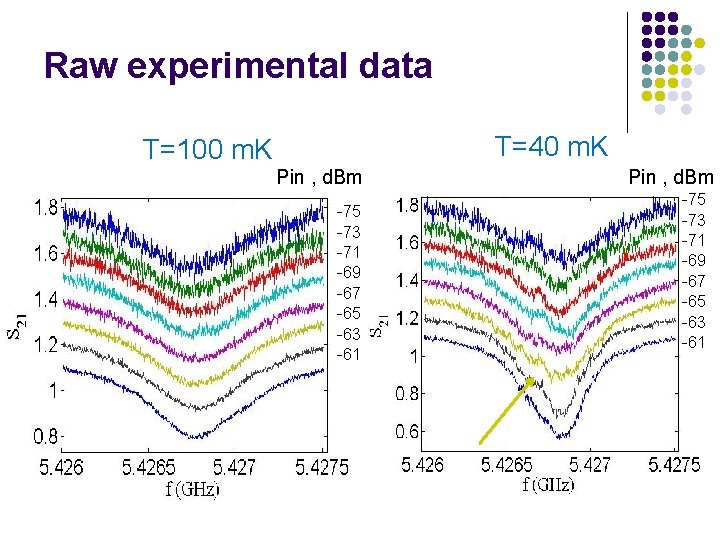
Raw experimental data T=40 m. K T=100 m. K Pin , d. Bm -75 -73 -71 -69 -67 -65 -63 -61

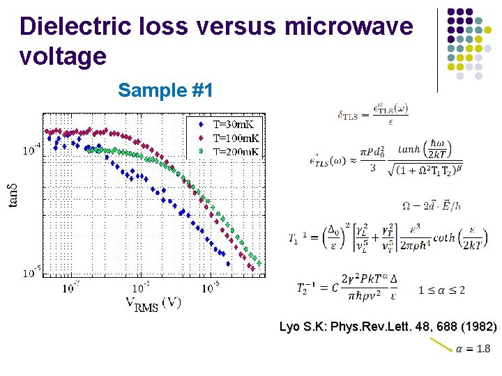
Dielectric loss versus microwave voltage Sample #1 Lyo S. K: Phys. Rev. Lett. 48, 688 (1982)

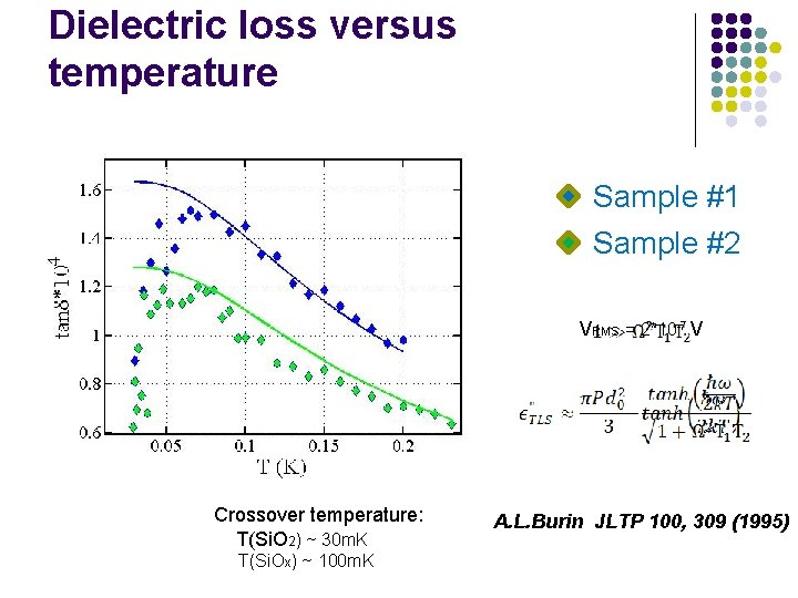
Dielectric loss versus temperature Sample #1 Sample #2 VRMS = 2*10 -7 V Crossover temperature: T(Si. O 2) ~ 30 m. K T(Si. Ox) ~ 100 m. K A. L. Burin JLTP 100, 309 (1995)

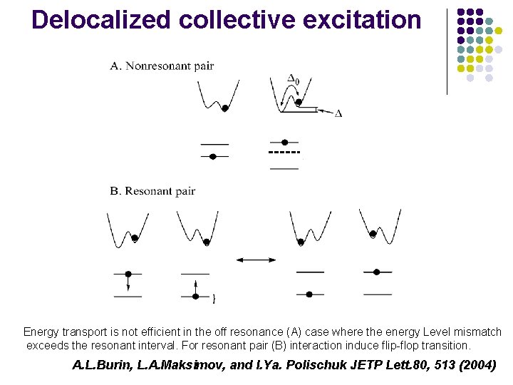
Delocalized collective excitation Energy transport is not efficient in the off resonance (A) case where the energy Level mismatch exceeds the resonant interval. For resonant pair (B) interaction induce flip-flop transition. A. L. Burin, L. A. Maksimov, and I. Ya. Polischuk JETP Lett. 80, 513 (2004)

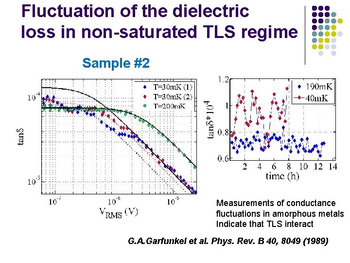
Fluctuation of the dielectric loss in non-saturated TLS regime Sample #2 Measurements of conductance fluctuations in amorphous metals Indicate that TLS interact G. A. Garfunkel et al. Phys. Rev. B 40, 8049 (1989)

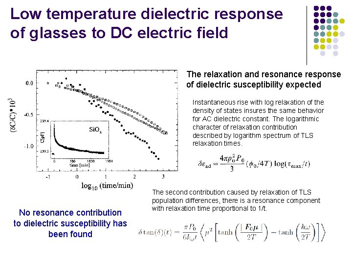
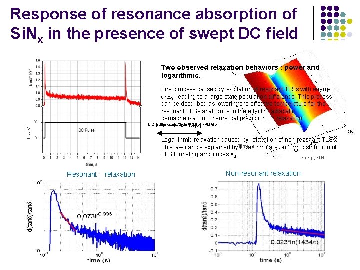
Low temperature dielectric response of glasses to DC electric field The relaxation and resonance response of dielectric susceptibility expected Instantaneous rise with log relaxation of the density of states insures the same behavior for AC dielectric constant. The logarithmic character of relaxation contribution described by logarithm spectrum of TLS relaxation times. No resonance contribution to dielectric susceptibility has been found The second contribution caused by relaxation of TLS population differences, there is a resonance component with relaxation time proportional to 1/t.

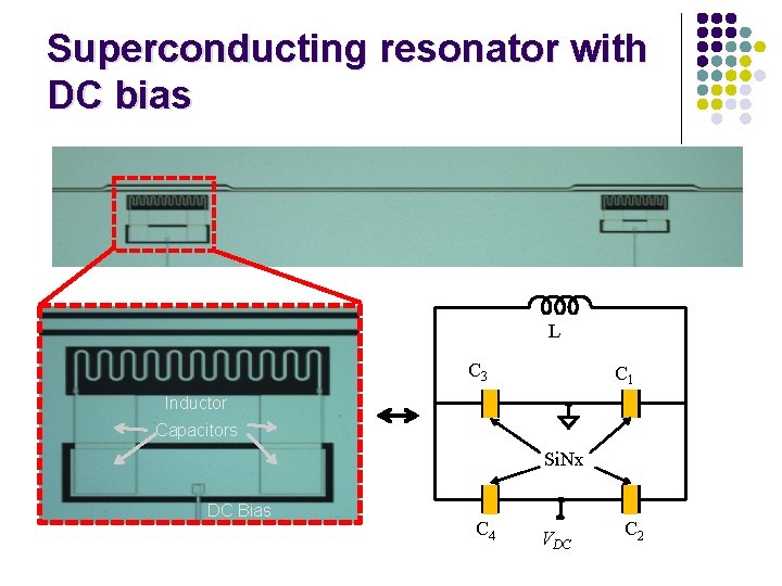
Superconducting resonator with DC bias L C 3 C 1 Inductor Capacitors Si. Nx DC Bias C 4 VDC C 2

Response of resonance absorption of Si. Nx in the presence of swept DC field Two observed relaxation behaviors : power and S 21 logarithmic. First process caused by excitation of resonant TLSs with energy ~ 0 leading to a large state population difference. This process can be described as lowering the effective temperature for the resonant TLSs analogous to the effect of adiabatic demagnetization. Theoretical prediction for relaxation DC pulse amplitude = 20 V ~. 40 MV/m time is ~1/t[2] UDC, V 20 0 Logarithmic relaxation caused by relaxation of non-resonant TLSs. s This law can be explained by. Time, logarithmically uniform distribution of TLS tunneling amplitudes 0. Freq. , GHz Resonant relaxation Non-resonant relaxation

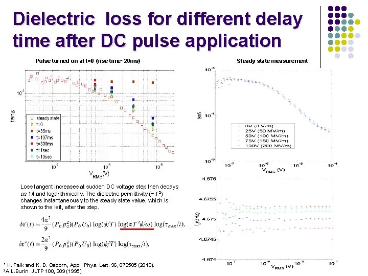
Dielectric loss for different delay time after DC pulse application Pulse turned on at t=0 (rise time~20 ms) Loss tangent increases at sudden DC voltage step then decays as 1/t and logarithmically. The dielectric permittivity (~ f-2) changes instantaneously to the steady state value, which is shown to the left, after the step. 1 H. Paik and K. D. Osborn, Appl. Phys. Lett. 96, 072505 (2010). JLTP 100, 309 (1995) 2 A. L. Burin Steady state measurement

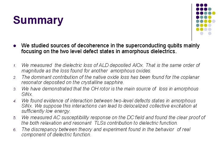
Summary l We studied sources of decoherence in the superconducting qubits mainly focusing on the two level defect states in amorphous dielectrics. 1. We measured the dielectric loss of ALD deposited Al. Ox. That is the same order of magnitude as the loss found for another amorphous oxides. The dominant contribution of the native oxide loss has been found for the coplanar resonator deposited on the crystalline sapphire. We have demonstrated that the OH rotor is the main source of loss in amorphous Si. Nx. We found evidence of interaction between two-level defects states in amorphous Si. Nx. We suppose this interactions can lead to delocalized collective excitation at sufficiently low energy. We measured AC susceptibility response on the DC field and found the clear proof of the both relaxation and resonant TLSs contribution to dielectric function. The discrepancy between theory and experiment found in the behavior of real component of dielectric function. 2. 3. 4. 5. 6.

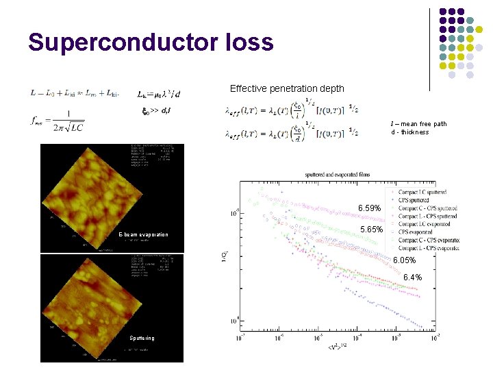
Superconductor loss Effective penetration depth 0 >> d, l l – mean free path d - thickness 6. 59% E-beam evaporation 5. 65% 6. 05% 6. 4% Sputtering

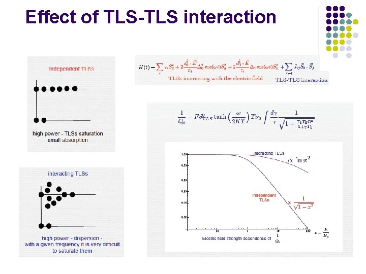
Effect of TLS-TLS interaction