Advanced Manufacturing Choices ENG 165 265 Spring 2017


- Slides: 37
Advanced Manufacturing Choices ENG 165 -265 Spring 2017, Class 6 Photolithography 12/1/2020
Content • • • • Lithography definitions Resist tone Introduction to the lithography process Surface Preparation Photoresist Application Soft Bake Align & Expose Develop Hard Bake Inspection Etch Layer or Add Layer Resist Stripping Final Inspection C-MEMS LIGA Clean- Room, Wafer Cleaning 12/1/2020 • CD and Tg • Making a Mask • Moore’s ‘Law’
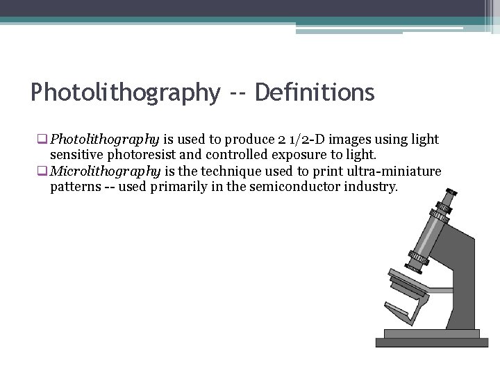
Photolithography -- Definitions q Photolithography is used to produce 2 1/2 -D images using light sensitive photoresist and controlled exposure to light. q Microlithography is the technique used to print ultra-miniature patterns -- used primarily in the semiconductor industry.
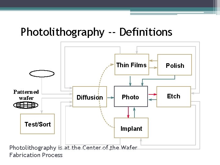
Photolithography -- Definitions Patterned wafer Test/Sort Diffusion Thin Films Polish Photo Etch Implant Photolithography is at the Center of *the Wafer Fabrication Process
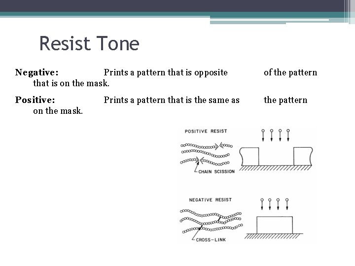
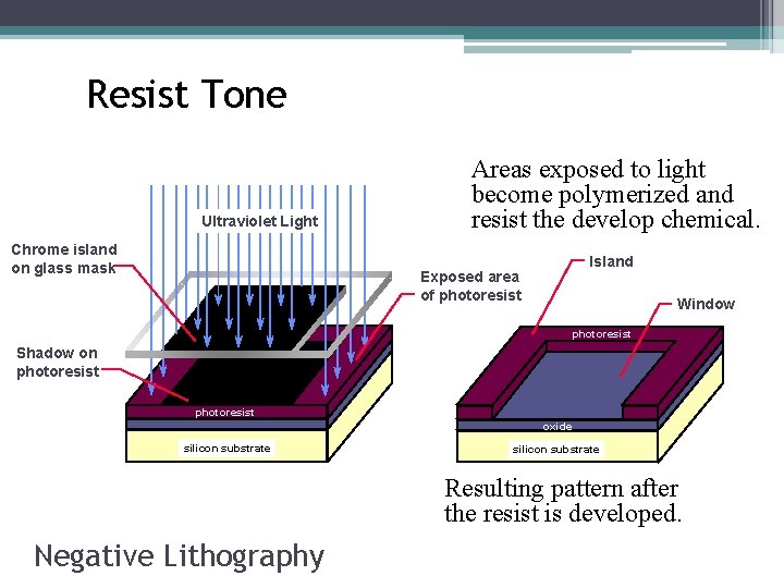
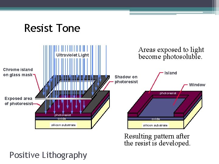
Resist Tone Negative: Prints a pattern that is opposite that is on the mask. of the pattern Positive: on the mask. the pattern Prints a pattern that is the same as
Resist Tone Ultraviolet Light Chrome island on glass mask Areas exposed to light become polymerized and resist the develop chemical. Island Exposed area of photoresist Window photoresist Shadow on photoresist oxide silicon substrate Resulting pattern after the resist is developed. Negative Lithography
Resist Tone Areas exposed to light become photosoluble. Ultraviolet Light Chrome island on glass mask Island Shadow on photoresist Window photoresist Exposed area of photoresist oxide silicon substrate Resulting pattern after the resist is developed. Positive Lithography
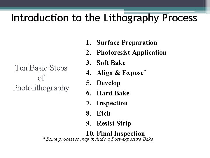
Introduction to the Lithography Process Ten Basic Steps of Photolithography 1. Surface Preparation 2. Photoresist Application 3. Soft Bake 4. Align & Expose* 5. Develop 6. Hard Bake 7. Inspection 8. Etch 9. Resist Strip 10. Final Inspection * Some processes may include a Post-exposure Bake
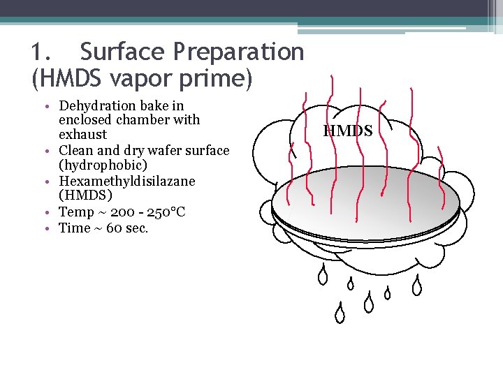
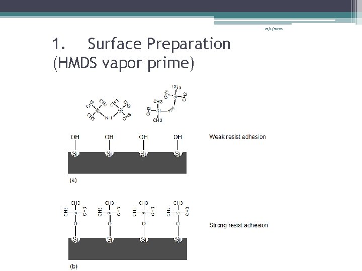
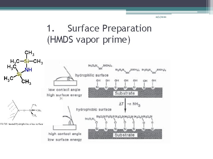
1. Surface Preparation (HMDS vapor prime) • Dehydration bake in enclosed chamber with exhaust • Clean and dry wafer surface (hydrophobic) • Hexamethyldisilazane (HMDS) • Temp ~ 200 - 250°C • Time ~ 60 sec. HMDS
12/1/2020 1. Surface Preparation (HMDS vapor prime)
12/1/2020 1. Surface Preparation (HMDS vapor prime)
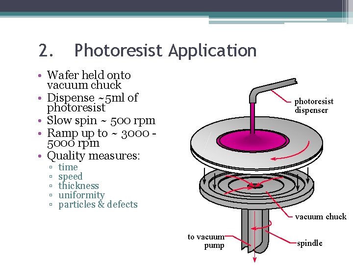
2. Photoresist Application • Wafer held onto vacuum chuck • Dispense ~5 ml of photoresist • Slow spin ~ 500 rpm • Ramp up to ~ 3000 5000 rpm • Quality measures: ▫ ▫ ▫ photoresist dispenser time speed thickness uniformity particles & defects vacuum chuck to vacuum pump spindle
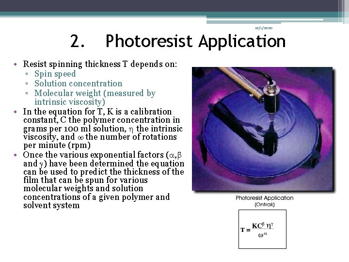
12/1/2020 2. Photoresist Application • Resist spinning thickness T depends on: ▫ Spin speed ▫ Solution concentration ▫ Molecular weight (measured by intrinsic viscosity) • In the equation for T, K is a calibration constant, C the polymer concentration in grams per 100 ml solution, h the intrinsic viscosity, and w the number of rotations per minute (rpm) • Once the various exponential factors (a, b and g) have been determined the equation can be used to predict the thickness of the film that can be spun for various molecular weights and solution concentrations of a given polymer and solvent system
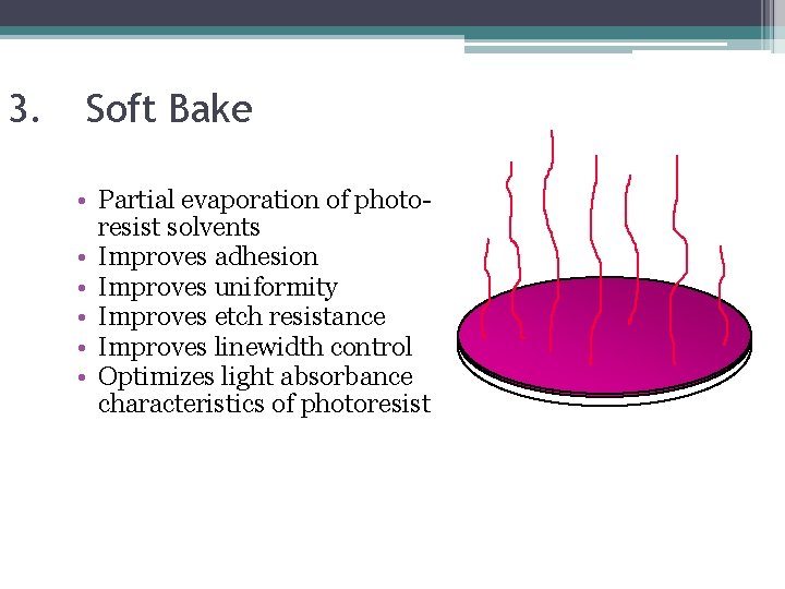
3. Soft Bake • Partial evaporation of photoresist solvents • Improves adhesion • Improves uniformity • Improves etch resistance • Improves linewidth control • Optimizes light absorbance characteristics of photoresist
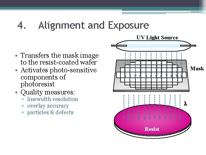
4. Alignment and Exposure UV Light Source • Transfers the mask image to the resist-coated wafer • Activates photo-sensitive components of photoresist • Quality measures: Mask ▫ linewidth resolution ▫ overlay accuracy ▫ particles & defects Resist
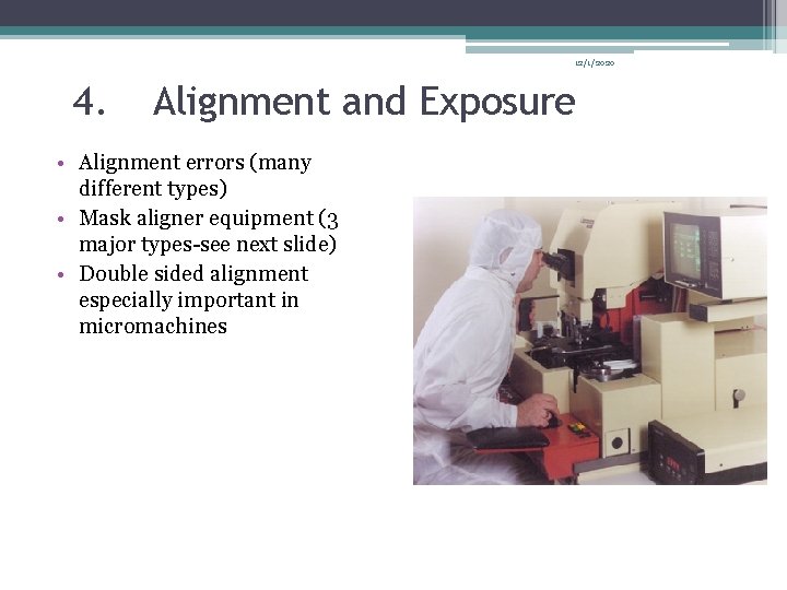
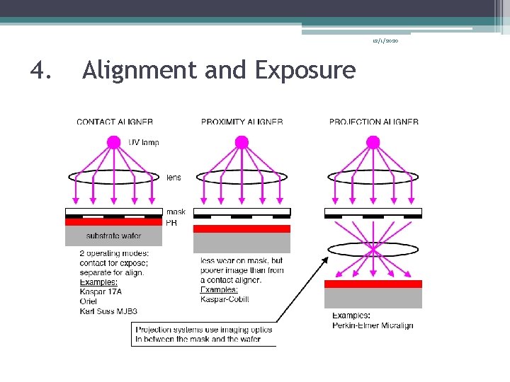
12/1/2020 4. Alignment and Exposure • Alignment errors (many different types) • Mask aligner equipment (3 major types-see next slide) • Double sided alignment especially important in micromachines
12/1/2020 4. Alignment and Exposure
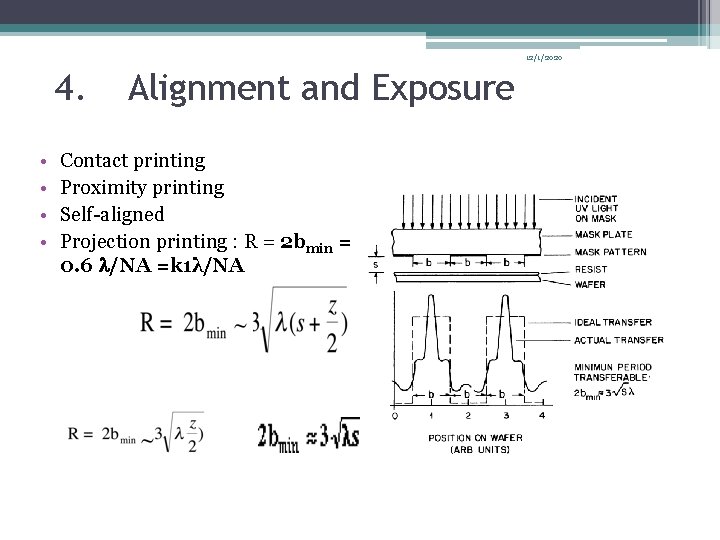
12/1/2020 4. • • Alignment and Exposure Contact printing Proximity printing Self-aligned Projection printing : R = 2 bmin = 0. 6 /NA =k 1λ/NA
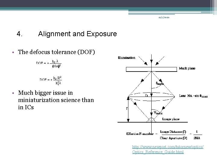
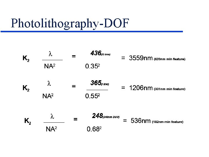
12/1/2020 4. Alignment and Exposure • The defocus tolerance (DOF) • Much bigger issue in miniaturization science than in ICs http: //www. newport. com/tutornew/optics/ Optics_Reference_Guide. html
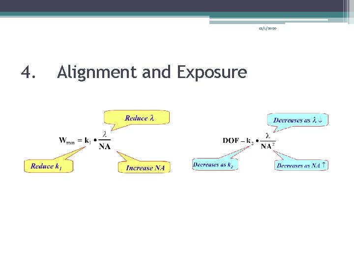
12/1/2020 4. Alignment and Exposure
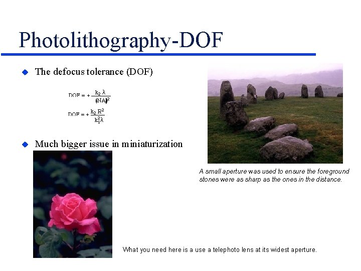
Photolithography-DOF u The defocus tolerance (DOF) u Much bigger issue in miniaturization science than in ICs A small aperture was used to ensure the foreground stones were as sharp as the ones in the distance. What you need here is a use a telephoto lens at its widest aperture.
Photolithography-DOF
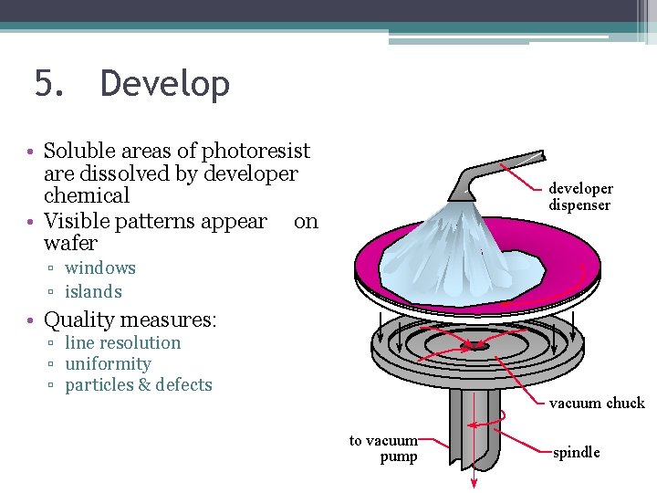
5. Develop • Soluble areas of photoresist are dissolved by developer chemical • Visible patterns appear on wafer developer dispenser ▫ windows ▫ islands • Quality measures: ▫ line resolution ▫ uniformity ▫ particles & defects vacuum chuck to vacuum pump spindle
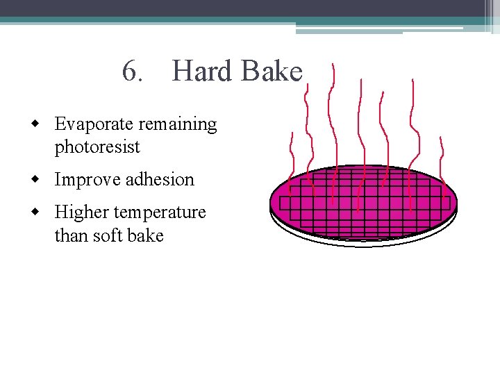
6. Hard Bake w Evaporate remaining photoresist w Improve adhesion w Higher temperature than soft bake
7. Development Inspection • Optical or SEM metrology • Quality issues: ▫ particles ▫ defects ▫ critical dimensions ▫ linewidth resolution ▫ overlay accuracy
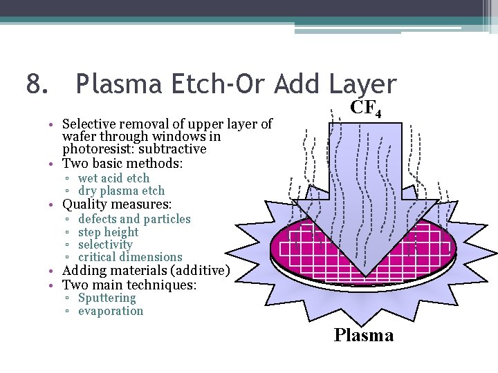
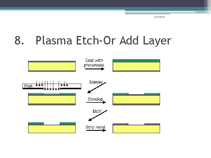
8. Plasma Etch-Or Add Layer • Selective removal of upper layer of wafer through windows in photoresist: subtractive • Two basic methods: CF 4 ▫ wet acid etch ▫ dry plasma etch • Quality measures: ▫ ▫ defects and particles step height selectivity critical dimensions • Adding materials (additive) • Two main techniques: ▫ Sputtering ▫ evaporation Plasma
12/1/2020 8. Plasma Etch-Or Add Layer
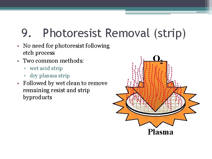
9. Photoresist Removal (strip) • No need for photoresist following etch process • Two common methods: ▫ wet acid strip ▫ dry plasma strip • Followed by wet clean to remove remaining resist and strip byproducts O 2 Plasma
10. Final Inspection • Photoresist has been completely removed • Pattern on wafer matches mask pattern (positive resist) • Quality issues: ▫ ▫ defects particles step height critical dimensions
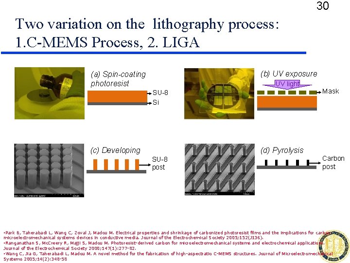
30 Two variation on the lithography process: 1. C-MEMS Process, 2. LIGA (b) UV exposure (a) Spin-coating photoresist UV light Mask SU-8 Si (c) Developing (d) Pyrolysis SU-8 post Carbon post • Park B, Taherabadi L, Wang C, Zoval J, Madou M. Electrical properties and shrinkage of carbonized photoresist films and the implications for carbon microelectromechanical systems devices in conductive media. Journal of the Electrochemical Society 2005; 152(J 136). • Ranganathan S, Mc. Creery R, Majji S, Madou M. Photoresist-derived carbon for microelectromechanical systems and electrochemical applications. Journal of the Electrochemical Society 2000; 147(1): 277 -82. • Wang C, Jia G, Taherabadi L, Madou M. A novel method for the fabrication of high-aspectratio C-MEMS structures. Journal of Microelectromechanical Systems 2005; 14(2): 348 -58
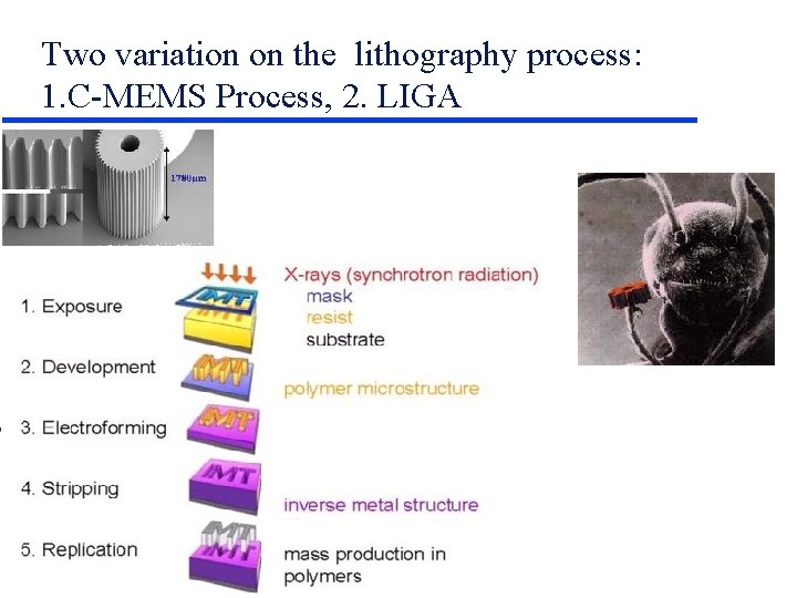
Two variation on the lithography process: 1. C-MEMS Process, 2. LIGA
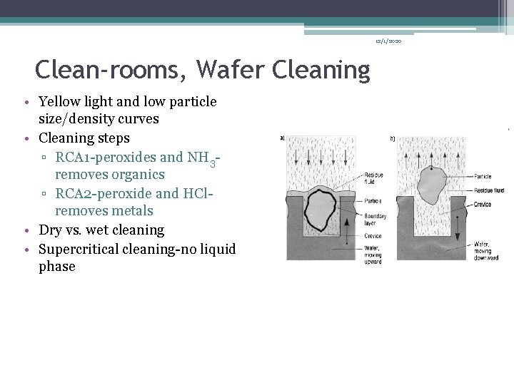
12/1/2020 Clean-rooms, Wafer Cleaning • Yellow light and low particle size/density curves • Cleaning steps ▫ RCA 1 -peroxides and NH 3 removes organics ▫ RCA 2 -peroxide and HClremoves metals • Dry vs. wet cleaning • Supercritical cleaning-no liquid phase
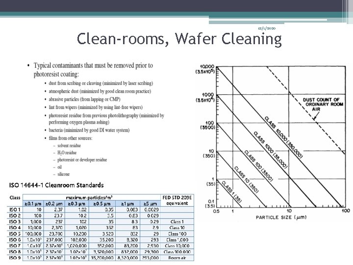
12/1/2020 Clean-rooms, Wafer Cleaning
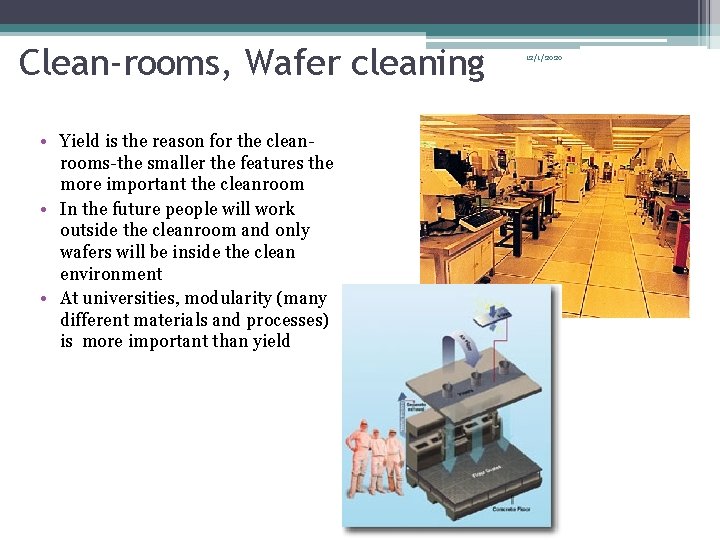
Clean-rooms, Wafer cleaning • Yield is the reason for the cleanrooms-the smaller the features the more important the cleanroom • In the future people will work outside the cleanroom and only wafers will be inside the clean environment • At universities, modularity (many different materials and processes) is more important than yield 12/1/2020
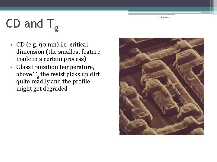
CD and Tg • CD (e. g. 90 nm) i. e. critical dimension (the smallest feature made in a certain process) • Glass transition temperature, above Tg the resist picks up dirt quite readily and the profile might get degraded 12/1/2020
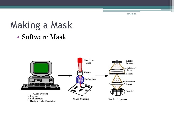
12/1/2020 Making a Mask • Software Mask
12/1/2020 Moore’s ‘Law’ • Observation and self fulfilling prophecy --not a physical law • Is it running out of steam?