Advanced Computation Modeling Yia Chung Chang Nanostructure electronics





- Slides: 39

Advanced Computation& Modeling 張亞中 (Yia. Chung Chang) – Nanostructure electronics & photonics 馬尚德 (Alec Maassen van den Brink)– Quantum computing 謝東翰(Tung-Han Hsieh) – Web computing New Hire: Shu-Wei Chang 關肇正 (Chao-Cheng Kaun)– Ab initio transport Vladimir Nazarov-CDFT -Nanophotonics

Missions l To carry out theoretical modeling in targeted areas of importance in applied sciences, including: 1) Nanostructure optoelectronic devices 2) Quantum information devices 3) Optical metrology and nanophotonics l Provide theoretical guidance and analysis to experimental groups within RCAS

Progress in Nanophotonics • • • Efficiency Enhancement of Ga. As Photovoltaics Employing Antireflective Indium Tin Oxide Nanocolumns, (with P. Yu, NCTU) [ Adv. Mater. , 20, 1– 4 (2008); Y. Z. Hsu Scientific Paper Award, 2010] Aspect-ratio-dependent ultra-low reflection and luminescence of dry-etched Si nanopillars on Si substrate [Nanotechnology, 20, 035303, (2009)] Spatial filtering by using cascading plasmonic gratings [Optics Express 17, 6218 (2009). ] Effective dielectric properties of biological cells: Generalization of the spectral density function approach [J. Phys. Chem. B 113 (29), 9924– 9931 (2009)] Dielectric response of Al. Sb from 0. 7 to 5. 0 e. V determined by in situ ellipsometry [Appl. Phys. Lett. 94, 231913 (2009)] T-shaped plasmonic array as a narrow-band thermal emitter or biosensor [Optics Exp. 17, 13526 -31 (2009)] Interband transitions of In. Asx. Sb 1−x alloy films [Appl. Phys. Lett. 95, 111902 (2009)] Manipulative depolarization and reflectance spectra of morphologically controlled nano-pillars and nano-rods [Optics Exp. , 17, 20824 -32 (2009)] Optical metrology of randomly-distributed Au colloids on a multilayer film [Optics Exp. 18, 1310 -15 (2010)] Plasmon-polariton band structures of asymmetric T-shaped plasmonic gratings [Optics Exp. 18, 2509 -14 (2010)] Surface plasmon resonance ellipsometry based sensor for studying biomolecular interaction [Biosensors and Bioelectronics 25, 2633 (2010)]

Research progress in nanoelectronics l Superconducting nanowires: Interplay of discrete transverse modes with supercurrent (Kaun)[Phys. Rev. B 80, 024513 (2009)] l Submonolayer quantum dot infrared photodetector [Appl. Phys. Lett. 94, 1 (2009)] l Bistable states of quantum dot array junctions for high-density memory [Jpn. J. Appl. Phys. , 48, 104504 (2009)] l Cesium doped and undoped Zn. O Nanocrystalline thin films: a comparative study of structural and Micro-Raman investigation of optical phonons, R. Thangavel [J. Ram. Spect. DOI 10. 1002/jrs. 2599 (2010)] l Surface States/Modes in One-Dimensional Semi-infinite Crystals, [Annals of Physics 325, 937 -947 (2010)] l Thermoelectric and thermal rectification properties of quantum dot junctions, [Phys. Rev. B 81, 205321 (2010)]

Progress in DFT & quantum structures l Exact dynamical exchange-correlation kernel of a weakly inhomogeneous electron gas [Phys. Rev. Lett. , 102, 113001 (2009)] l Open a way for interpolation between low- and high frequency behavior of the xc kernel of an arbitrary system by expressing it in the high-frequency limit through a few ground-state properties. (Nazarov) [Phys. Rev. B 81, 245101 (2010)] l On the relation between the scalar and tensor exchange-correlation kernels of the time-dependent density-functional theory [J. Chem. Phys. . in press (2010) l Enhancement factor, electrostatic force and emission current in nanoneedle emitter [Euro Phys. Lett. 85, 17001 (2009) ] l Field enhancement factor and field emission from a hemi-ellipsoidal metallic needle [Ultramicroscopy 109, 373 (2009)] l Van der Waals interaction between two crossed carbon nanotubes [ACS nano, in press (2010)] l Corrected field enhancement factor for the floating sphere model of carbon nanotube emitter [J. Appl. Phys. , in press (2010)] l Development of GPU computing environment and Investigation of the novel "Adaptive Thick Restart Lanczos Algorithm" for low-lying eigenmode projection for large sparse Hermition matrix. (TH Hsieh)

Optical nanometrology l. Nanometrology allows optical inspection of the geometry of nanostructures down to 10 nm scale. l. It uses a best fit to the measured ellipsometric spectra via theoretical simulation (with efficient software) to determine the critical dimension. l. If done correctly, one can reconstruct images of nm resolution by using an optical instrument (with wavelengths 100 nm-1000 nm). l. It is noninvasive and capable of probing buried structures and biological systems

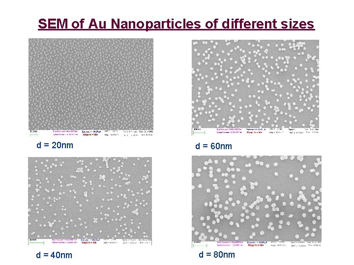
SEM of Au Nanoparticles of different sizes d = 20 nm d = 40 nm d = 60 nm d = 80 nm

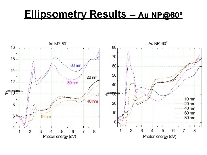
Ellipsometry Results – Au NP@60 o

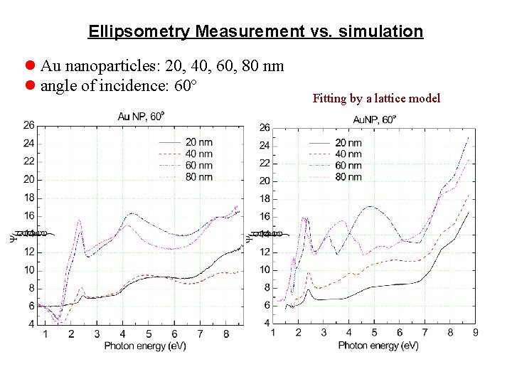
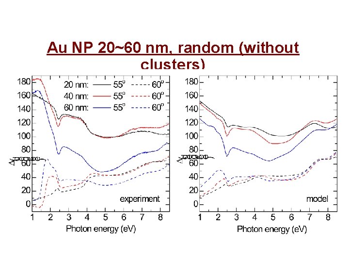
Ellipsometry Measurement vs. simulation l Au nanoparticles: 20, 40, 60, 80 nm l angle of incidence: 60º Fitting by a lattice model

Effects of Site Disorder ∫ f

Simplified model for structure factor S(g) = 1 + f ∑j≠ 0 exp{i (k-k 0) ∙Rj} L = 1+ f 2π ∫a rdr J 0(gr) /Ac = 1 + f [Nδk, k 0 – 2π(a 2/Ac)J 1(ga) /ga], f = similarity factor N= total number of atoms considered, g = k - k 0 Ac = average cell volume [S. -H. Hsu, Y. -C. Chang*, Y. -C. Chen, P. -K. Wei, Y. D. Kim, Optics Exp. 18, 1310 (2010)]

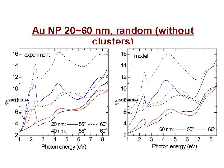
Au NP 20~60 nm, random (without clusters)

Au NP 20~60 nm, random (without clusters)

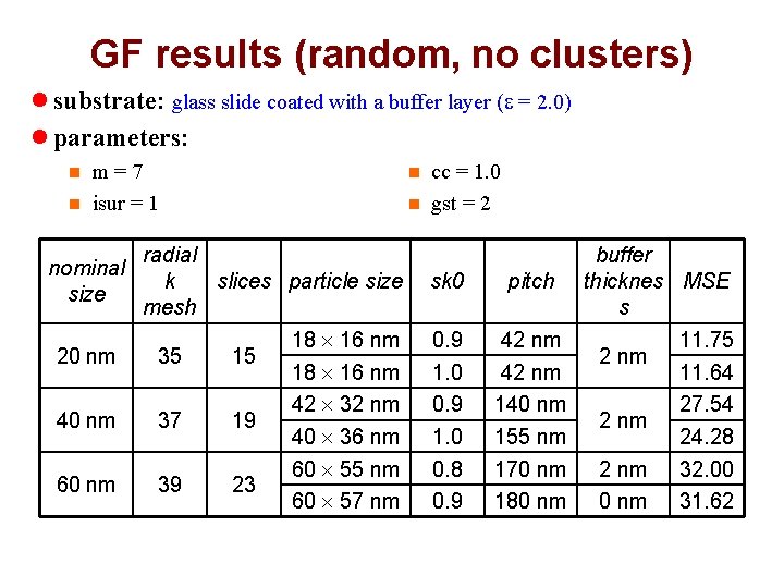
GF results (random, no clusters) l substrate: glass slide coated with a buffer layer (e = 2. 0) l parameters: m=7 n isur = 1 n nominal size 20 nm 40 nm 60 nm radial k slices particle size mesh 18 16 nm 35 15 18 16 nm 42 32 nm 37 19 40 36 nm 60 55 nm 39 23 60 57 nm cc = 1. 0 n gst = 2 n sk 0 pitch 0. 9 1. 0 0. 8 0. 9 42 nm 140 nm 155 nm 170 nm 180 nm buffer thicknes MSE s 11. 75 2 nm 11. 64 27. 54 2 nm 24. 28 2 nm 32. 00 0 nm 31. 62

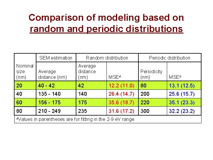
Comparison of modeling based on random and periodic distributions SEM estimation Random distribution Nominal size Average (nm) distance (nm) Average distance (nm) 20 40 - 42 40 Periodic distribution MSEa Periodicity (nm) MSEa 42 12. 2 (11. 0) 80 13. 1 (12. 5) 135 - 140 26. 4 (14. 7) 200 25. 6 (15. 7) 60 156 - 175 35. 6 (18. 7) 220 35. 1 (23. 3) 80 210 - 249 235 31. 6 (17. 2) 300 32. 2 (23. 2) a. Values in parentheses are for fitting in the 2 -9 e. V range.

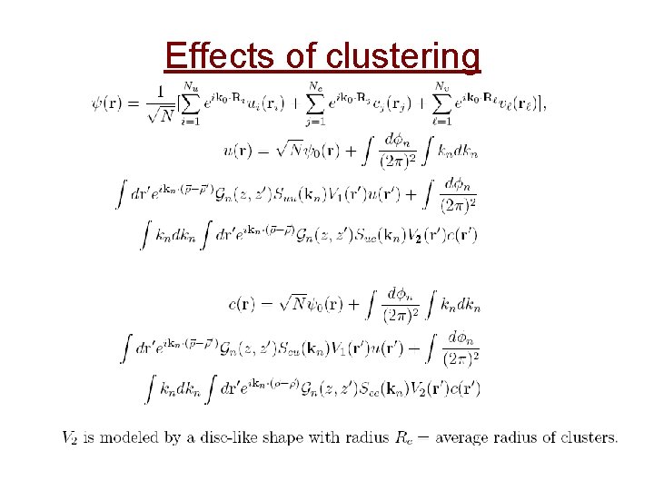
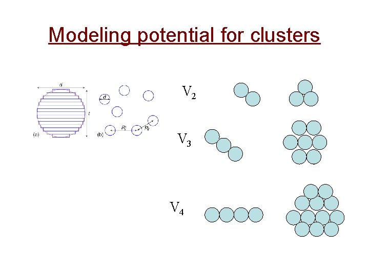
Effects of clustering 2

Modeling potential for clusters V 2 V 3 V 4

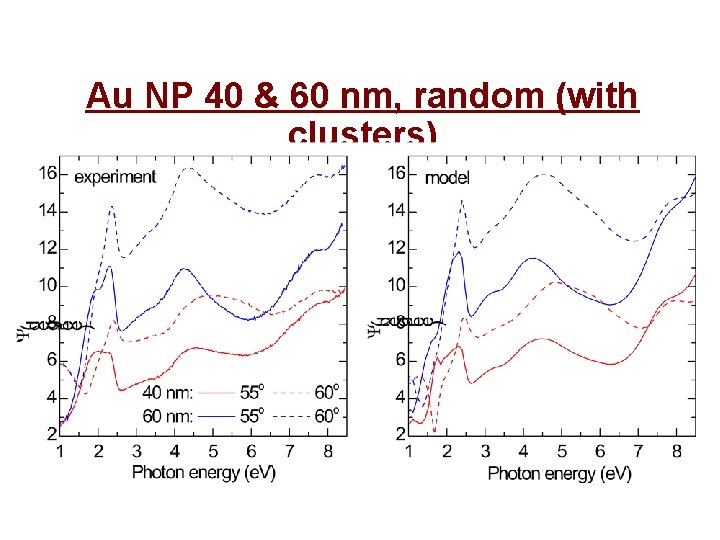
Au NP 40 & 60 nm, random (with clusters)

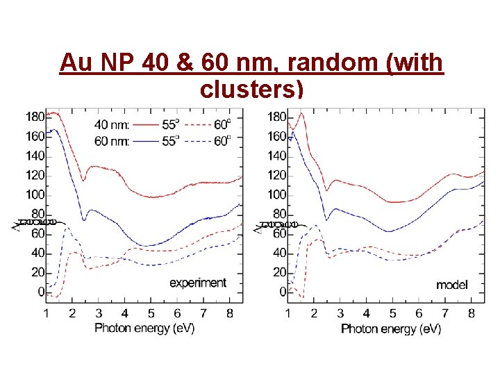
Au NP 40 & 60 nm, random (with clusters)

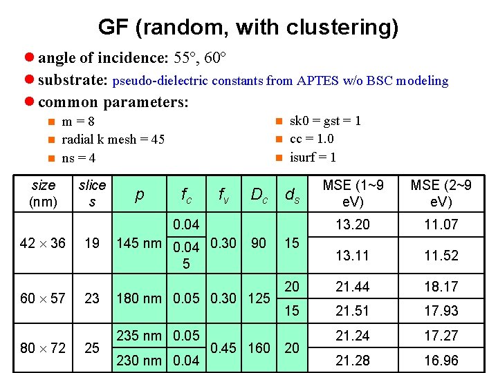
GF (random, with clustering) l angle of incidence: 55º, 60º l substrate: pseudo-dielectric constants from APTES w/o BSC modeling l common parameters: sk 0 = gst = 1 n cc = 1. 0 n isurf = 1 m=8 n radial k mesh = 45 n ns = 4 n n size (nm) slice s p fc fv Dc MSE (1~9 e. V) MSE (2~9 e. V) 13. 20 11. 07 13. 11 11. 52 20 21. 44 18. 17 15 21. 51 17. 93 21. 24 17. 27 21. 28 16. 96 ds 0. 04 42 36 60 57 80 72 19 23 25 145 nm 0. 04 0. 30 5 90 180 nm 0. 05 0. 30 125 235 nm 0. 05 230 nm 0. 04 0. 45 160 15 20

Summary l. Samples with different sizes of Gold nanoparticles immobilized on a glass substrate are investigated by variable-angle spectroscopic ellipsometry (VASE) in the UV to near IR region. l. Both the Green’s function method and rigorous coupled-wave analysis (RCWA) were used to model the ellipsometric spectra l. GF method is 10 – 100 times more efficient than RCWA in most cases for lattice model calculation. l. For random scattering problem, only GF method is used, and it is faster by another order of magnitude. l. Our model calculations show reasonable agreement with the ellipsometric measurements. l. This demonstrates that the spectroscopic ellipsometry could be a useful tool to provide information about the size and distribution of nanoparticles deposited on insulating substrate. l. The technique can be extended to inspect buried nanostructures

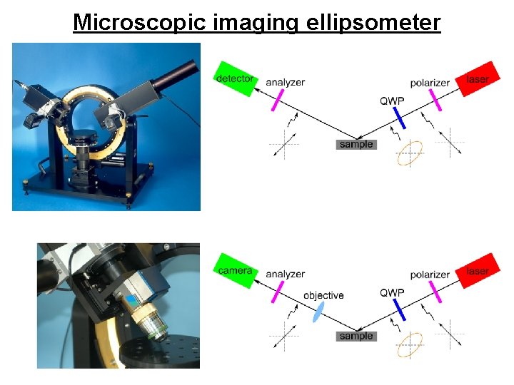
Microscopic imaging ellipsometer

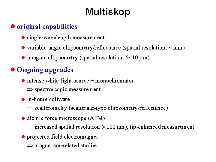
Multiskop l original capabilities l single-wavelength measurement l variable-angle ellipsometry/reflectance (spatial resolution: ~ mm) l imagine ellipsometry (spatial resolution: 5~10 mm) l Ongoing upgrades l intense white-light source + monochromator spectroscopic measurement l in-house software scatterometry (scattering-type ellipsometry/reflectance) l atomic force microscope (AFM) increased spatial resolution ( 100 nm), tip-enhanced measurement l projected-field electromagnet magnetism-related studies

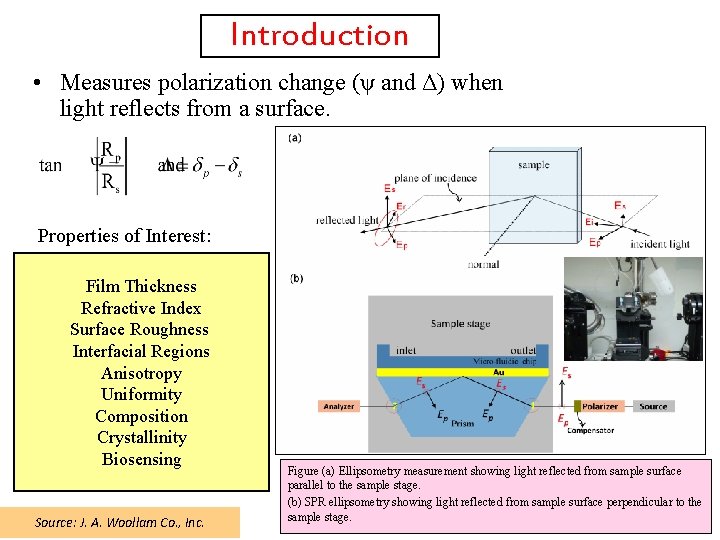
Introduction • Measures polarization change (ψ and Δ) when light reflects from a surface. Properties of Interest: Film Thickness Refractive Index Surface Roughness Interfacial Regions Anisotropy Uniformity Composition Crystallinity Biosensing Source: J. A. Woollam Co. , Inc. Figure (a) Ellipsometry measurement showing light reflected from sample surface parallel to the sample stage. (b) SPR ellipsometry showing light reflected from sample surface perpendicular to the sample stage.

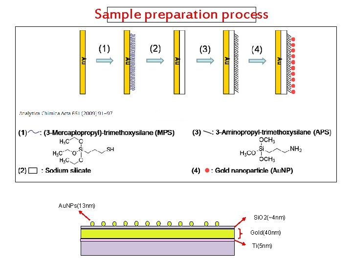
Sample preparation process Au. NPs(13 nm) Si. O 2(~4 nm) Gold(40 nm) Ti(5 nm)

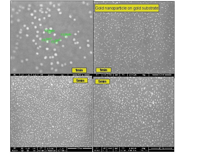
Gold nanoparticle on gold substrate 1 min 5 min

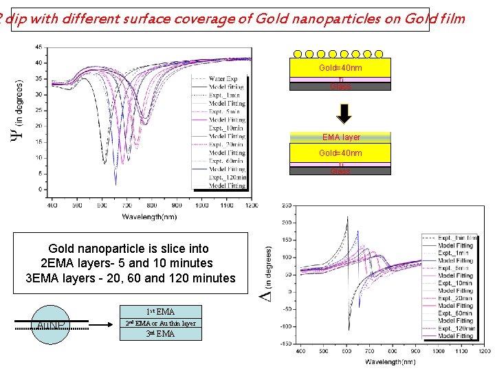
R dip with different surface coverage of Gold nanoparticles on Gold film Gold=40 nm Ti Glass EMA layer Gold=40 nm Ti Glass Gold nanoparticle is slice into 2 EMA layers- 5 and 10 minutes 3 EMA layers - 20, 60 and 120 minutes 1 st EMA Au. NP 2 nd EMA or Au thin layer 3 rd EMA

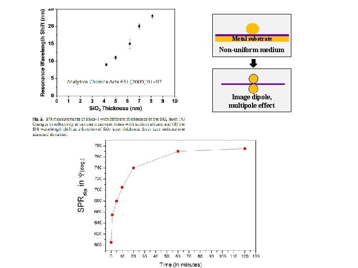
Metal substrate Non-uniform medium Image dipole, multipole effect

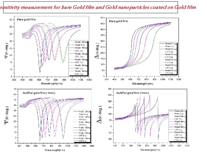
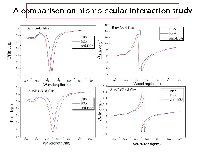
ensitivity measurement for bare Gold film and Gold nanoparticles coated on Gold film Bare gold film Au. NPs/ gold film (1 min)

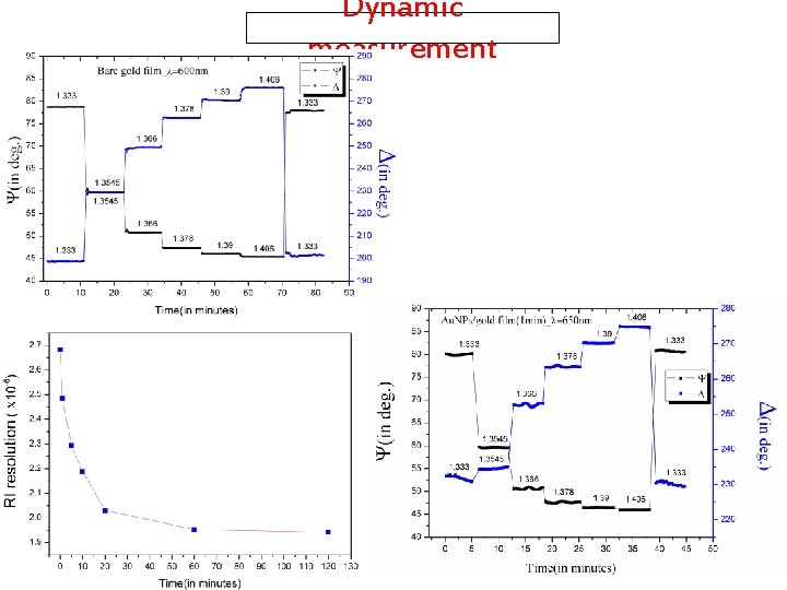
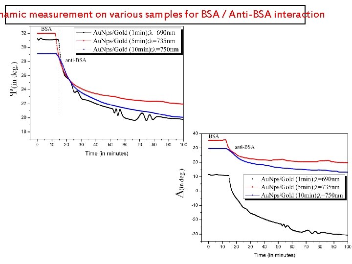
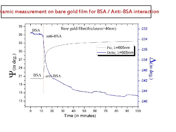
Dynamic measurement

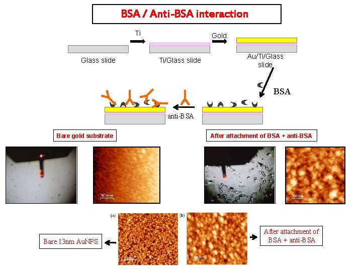
BSA / Anti-BSA interaction Ti Glass slide Gold Ti/Glass slide Au/Ti/Glass slide BSA anti-BSA Bare gold substrate Bare 13 nm Au. NPS After attachment of BSA + anti-BSA

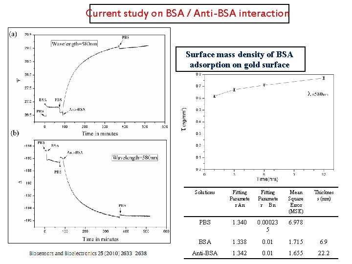
Current study on BSA / Anti-BSA interaction Surface mass density of BSA adsorption on gold surface Solutions Fitting Paramete r An Fitting Paramete r Bn Mean Square Error (MSE) Thicknes s (nm) PBS 1. 340 0. 00023 5 6. 978 BSA 1. 338 0. 01 1. 715 6. 9 Anti-BSA 1. 342 0. 01 1. 655 22. 2

namic measurement on various samples for BSA / Anti-BSA interaction

namic measurement on bare gold film for BSA / Anti-BSA interaction

A comparison on biomolecular interaction study

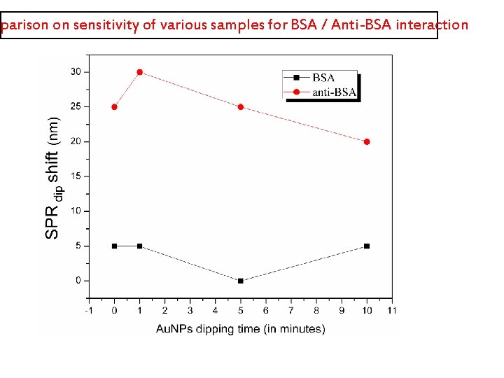
mparison on sensitivity of various samples for BSA / Anti-BSA interaction

Conclusion – A very simple and promising technique is presented and further extended its potential application to investigate both spectroscopic and real time response of bio-molecular interaction based on the ellipsometry optical signals. – Surface Plasmon Resonance(SPR) of the gold film can be tune with various distribution of Au. NPs coated on gold film. – Bulk refractive indices measurement shows that more densely packed Au. NPs on gold film give higher refractive index (RI) resolution. – However, local refractive index change corresponding to the adsorption of BSA and subsequent attachment of anti. BSA measurement shows that sample dipped in Au. NPs for 1 minute shows better sensitivity as compare to other dipping time as well as bare gold film. – Hence, direct correlation on sensitivity from bulk to local refractive index change is trivial and need further investigation. – SPR ellipsometry does make a unique tool to investigate various challenging issues in terms high affinity bio-

Application software development • LED/light scattering Simulator: Optical simulation for LED devices and optical metrology. • LASTO package: An abinitio computation package based on Linear Augmented Slater-Type Orbitals basis. • Nanostructure Simulator: Effective bond-orbital method for microsopic strain distribution, electronic states, and optical properties of semiconductor nanostructures computatio • GPU software development (Hsieh)

Future goals of ACM group l. Development of multiscale modeling package for future generation nanoscale optoelectronic devices (combining modeling techniques for electron transport, interface characteristics, optical properties and heat dissipation. l. Couple theoretical modeling with experimental studies for development of novel nanometrology technology. l. Modeling for spintronics, quantum information, and magnetic RAM.