500 MHz SRF Cavity Development for Accelerating Muons

 – Proton")


 1 & 2 Cell")


 after combined RF and Helium processing • Eacc = 11")


 350 MHz LEP cavities 400 MHz")


 Nb-Cu and")


- Slides: 37
500 MHz SRF Cavity Development for Accelerating Muons Don Hartill CLASSE Cornell University Muon Accelerator Program Review Fermilab, August 25, 2010
Muon Collider Ingredients • Muon Collider comprises these sections (similar to NF) – Proton Driver • primary beam on production target – Target, Capture, and Decay • create ; decay into MERIT – Bunching and Phase Rotation • reduce E of bunch – Cooling • reduce long. and transverse emittance MICE 6 D experiment – Acceleration • 130 Me. V ~1 Te. V with RLAs, FFAGs or RCSs – Collider Ring • store for 500 turns Much of Muon Collider R&D is common with Neutrino Factory R&D
Acceleration Requirements § The highest possible Eacc to minimize muon decay § Large transverse and longitudinal acceptances Both requirements favor the choice of SRF § SRF cavities have a high Q 0 Pd = Eacc 2/((R/Q)Q 0) § SRF can achieve high gradients with modest RF power § SRF cavities accommodate a larger aperture without a large penalty for the low R/Q § Chose low frequency because of beam size § Chose low frequency to have high stored energy (bunch current)
History of 200 MHz Program • Collaboration formed in late 2000 to produce and test two 200 MHz • • Superconducting Cavities based on a CERN design National Science Foundation supported this program Two cavities were produced and tested One cavity performed well: Eacc > 11 MV/m Second cavity was limited by field emission at < 3 MV/m Second cavity demonstrated performance in Hext < 1200 Oe To save costs decided to move to 500 MHz with parallel effort to improve Nb sputter coatings and to fabricate cavities from explosion bonded and hot isostatic pressure bonded 1 mm thick Nb on 4 mm thick Cu Program was terminated in the fall of 2006 with the explosion bonded cavity awaiting final finishing
200 MHz Program Collaborators H. Padamsee R. Geng – now at JLAB P. Barnes J. Sears V. Shemelin J. Kaufman R. Losito E. Chiaveri H. Preis S. Calatroni E. Palmieri - INFN M. Pekelar - ACCEL G. Wu – JLAB – now at FNAL
Linac and RLA Cavity Layout Focusing Solenoid (2 -4 T) 1 & 2 Cell SRF cavities
Typical 201 MHz SRF Parameter List Linac RLA Hundreds of high-gradient 201 MHz cavities needed (along with hundreds of 402 MHz cavities needed for the higher energy sections)
Why Nb-Cu Cavities? § Save material cost § May save cost on magnetic field shielding (Rs of sputtered Nb may be less sensitive to residual magnetic field than bulk Nb) § May save cost on LHe inventory by pipe cooling (Brazing Cu pipe to Cu outer surface of cavity) 1. 5 GHz bulk Nb cavity (3 mm) material cost: ~ $ 2 k/cell 200 MHz: X (1500/200)2 = 56 $ 112 k/cell Thicker material (8 mm) needed: X 2. 7 $300 k/cell Nb Material (bulk Nb version) cost for 600 cells : 180 M$ Cu (OF) Material (sputter substrate) is x 40 cheaper: 5 M$ Nb-Cu Bonded Material: < 50 M$
Example of Pipe Cooling
First 201 -MHz Nb-Cu Cavity Major dia. : 1. 4 m 400 mm BT Cavity length: 2 m
Fabrication at CERN Electro-polished half cell • DC voltage: 400 -650 V • Gas pressure: 2 m. Torr • Substrate T: 100 °C • RRR = 11 • Tc = 9. 5 K Magnetron Nb film (1 -2 m) sputtering
First RF Test at Cornell Cavity on test stand Cavity going into test pit in Newman basement Pit: 5 m deep X 2. 5 m dia.
First Cavity Test Results
Two-point Multipacting • Two points symmetric about equator are involved • Spontaneously emitted electrons arrive at opposite point after T/2 • Accelerated electrons impact surface and release secondary electrons • Secondary electrons are in turn accelerated by RF field and impact again • The process will go on until the number of electrons are saturated MP electrons drain RF power a sharp Q drop
Two-point MP at 3 MV/m MULTIPAC simulation confirmed exp. observation Resonant trajectory of MP electrons It was possible to process through MP barrier
Third Cavity Test Q(Eacc) after combined RF and Helium processing • Eacc = 11 MV/m • Low field Q = 2 1010 Limited by RF coupler • 75% goal Eacc achieved • Q-slope larger than expected Q improves with lower T FE not dominant
Hext Effect on Cavity: Setup 2 T solenoid SC Nb/Ti coil 200 MHz cavity Layout of Linear Accelerator for n source • 2 -T solenoid needed for tight focusing • Solenoid and cavity fitted in one cryostat • Large aperture (460 mm) • Will cavity still work with Hext > 0 ? Cavity test in the presence of an Hext
Hext Effect on 2 nd Cavity Q stays intact up to Hext = 1200 Oe
Q-slope of Sputtered Film Nb Cavities § Q-slope is a result of material properties of film Nb Sputtered Nb § The Cu substrate (surface) has some influence § The exact Q-slope mechanism is not fully understood Bulk Nb
Sputtered Nb-Cu Cavities Q 0(X 1 E 9) 350 MHz LEP cavities 400 MHz LHC cavities Despite Q-slope, sputtered Nb-Cu cavities have achieved a 15 MV/m Eacc at 400 MHz
Expected Performance Projecting LHC 400 MHz to 200 MHz 200 MHz Empirical frequency dependence of Q-slope Measured Q-slope of 201 -MHz cavity is 10 times steeper than expected
Q-slope: Impact Angle Effect R 67 mm Impact angle of Nb atom: g 100 mm • CERN explored low b v/c) 350 MHz cavities • With the same cathode geometry, lower b low g
Q-slope: Impact Angle Effect Correlation: lower b lower g steeper Q-slope Need a more robust approach to maintain high Q needed for economy
Reducing Q-Slope § It is clear from the LEP cavity production that there is significant variation in Q slope and it is always present in magnetron sputtered Nb cavities. § To limit power requirements, both RF and cryogenic, Q slope must be reduced to a minimum. § Different sputtering techniques other than magnetron sputtering may yield better results. § The sputtered surface will always be a delicate feature. § Reproducibility will always be a problem. § Because of diffusion of Cu into Nb layer, low temperature bake known to help in solid Nb cavities is not possible.
Other Techniques for Nb Film Deposition § § § Bias sputtering Energetic deposition in vacuum Vacuum arc deposition Electron cyclotron resonance sputtering Prototypes of these techniques were developed but none were mature enough to produce a cavity. § Bond 1 mm thick Nb to 4 mm thick Cu by hot isostatic bonding or explosion bonding. § With all the challenges of Nb sputter coating decide to concentrate on using bonded Nb material. § Bonded Nb permits a low temperature bake.
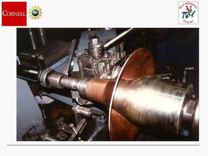
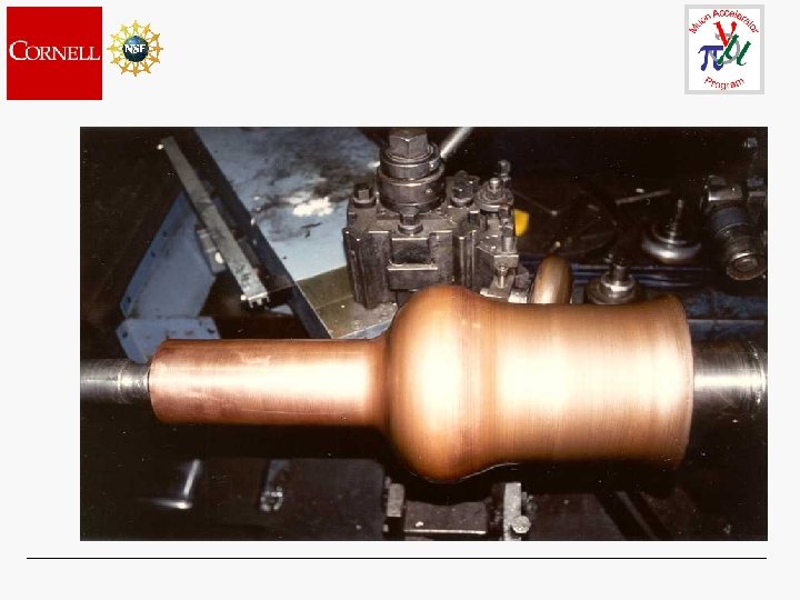
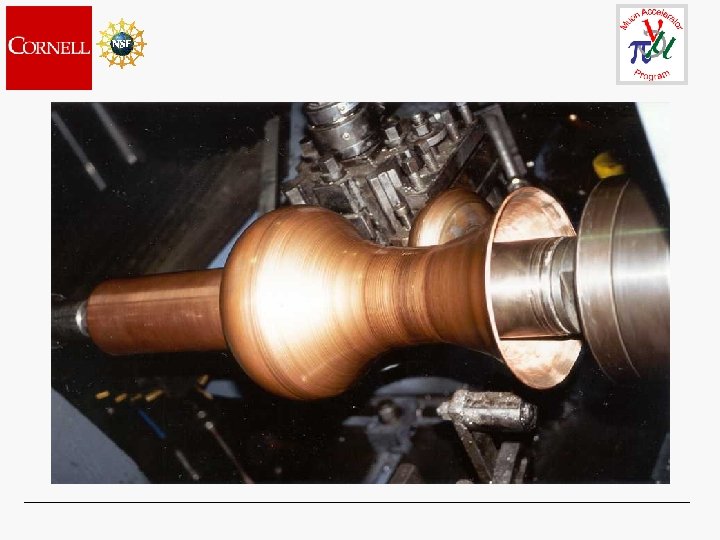
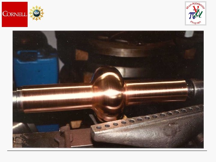
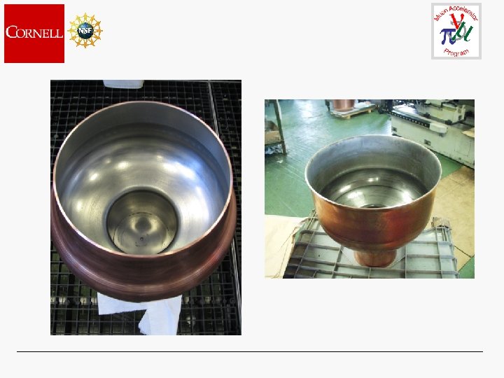
Spinning Cavities • A few slides illustrating the spinning process
Spinning of Bonded Nb-Cu § Both a hot isostatic pressure bonded (hipped) Nb-Cu and an explosion bonded Nb-Cu plate were spun into 500 MHz cavities. § The hipped material appeared to yield an excellent Nb inner surface after initial spinning. After annealing at 250°C, several small bubbles (10 mm 2) appeared indicating de-lamination of Nb from Cu. § Minor surface cracks were apparent in the cavity spun from the explosion bonded material. § With very light grinding and subsequent surface chemistry the cavity from explosion bonded material is likely to yield a cavity capable of > 17 MV/m accelerating gradient. The hipped cavity cannot be used because it would be thermally unstable in the bubble region. § A single cell 1300 MHz cavity spun from this material has achieved a 40 MV/m accelerating gradient.
Summary of Original Program § The first 201 -MHz SC cavities have been constructed. § Test results for the first cavity were Eacc = 11 MV/m with Q 0 = 2 1010 at low field. § MP barriers were present and could be processed through. § Cavity performance was not affected by Hext < 1200 Oe. § Some progress was made on the understanding of the Q-slope in sputtered cavities. § Currently a low temperature bake ~ 100°C seems to significantly reduce the Q slope in solid Nb cavities. This is not suitable for sputter-coated cavities because of the diffusion of Cu into the Nb layer. OK for the bonded material since Nb is 1 mm thick and diffusion rates are low.
Summary of Original Program § A 500 MHz cavity coated at ACCEL was assembled and tested twice to 4 MV/m with heavy field emission and quench. A second cavity reached 10 MV/m with large Q slope on its second test. § Recoated 201 MHz cavity #1 at CERN in 3/04 – peeling observed – recoated again, still bad – recoat again and retested with heavy field emission and quench – both cavities shipped back to CERN to avoid paying duty. § Used Auger surface analysis system and SIMS to further characterize sputtered Nb surfaces. Found that the oxygen level near the surface is an important player. § Spun cavities from bonded material were sent to ACCEL for flange installation.
Summary of Original Program § Cost of 1 mm Nb bonded to 4 mm of Cu is <1/3 that of 5 mm RRR 300 Nb sheet in small quantities for both hip and explosion bonding. § Program was terminated in the Fall of 2006.
Proposed Development Program • Program proposed to the National Science Foundation • Finish the explosion bonded cavity presently at Research Instruments. • Carry out surface preparation, chemistry and high pressure rinse. • Test the cavity taking advantage of the new helium recovery system and the new diagnostic technique based on second sound. This may be particularly interesting since these cavities have no equator weld zone. • Check sensitivity to external DC magnetic field. • Spin a new cavity from one of the remaining explosion bonded sheets at INFN. Pay particular attention to the annealing procedure to see if this influences the minor surface cracking. • Add flanges to the new cavity at Research Instruments. • Carry out surface preparation, chemistry and high pressure rinse. • Test the cavity.
Proposed Development Program • Order two sheets of explosion bonded material with thicker Nb (1. 5 to 2 mm) on 4 mm of Cu. • Spin a new cavity from the thicker material at INFN. • The thicker material may be less prone to minor surface cracking and if not, it provides more material to work with. • Add flanges at Research Instruments. • Carry out surface preparation, chemistry and high pressure rinse. • Test the cavity. • Check the sensitivity to external DC magnetic field. • Explore other possible construction techniques including electroplating Cu on a thin (1 to 2 mm) Nb cavity. • Assuming success of the 500 MHz program develop a proposal to construct and test a 200 MHz cavity using these same techniques.