TWEPP 22 nm CMOS vs 22 nm SOI


- Slides: 32

TWEPP 22 nm CMOS vs 22 nm SOI vs 16 nm Fin. FET BY SOFICS – BENJAMIN VAN CAMP 2020 -09 -22

CMOS vs SOI vs Fin. FETs • Introduction – Wafer Price – CMOS vs SOI vs Fin. FETS – TLP curve • ESD Design Window • ESD devices • Conclusion SOFICS © 2020 Proprietary & Confidential 2

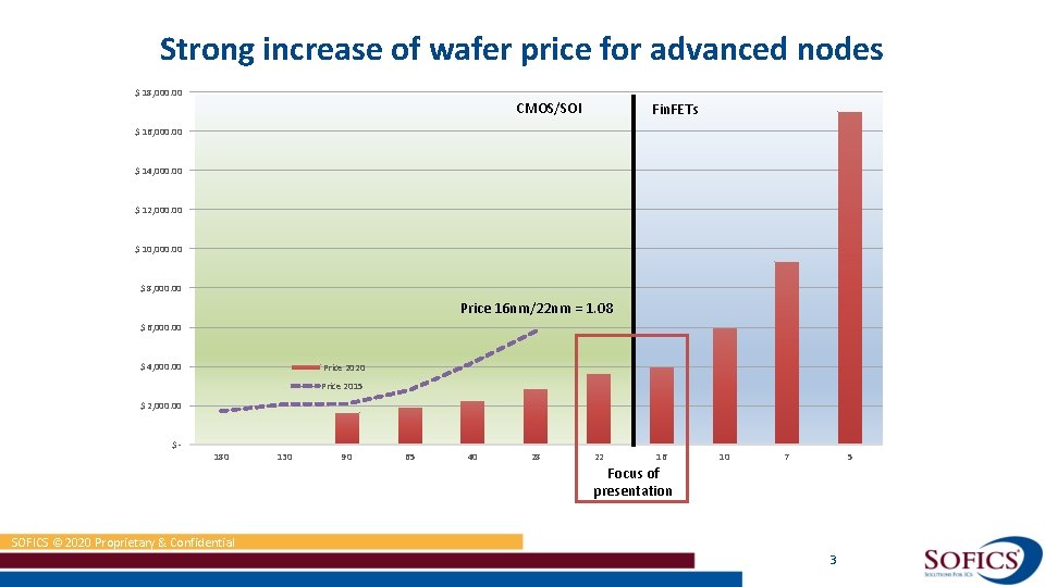
Strong increase of wafer price for advanced nodes $ 18, 000. 00 CMOS/SOI Fin. FETs $ 16, 000. 00 $ 14, 000. 00 $ 12, 000. 00 $ 10, 000. 00 $ 8, 000. 00 Price 16 nm/22 nm = 1. 08 $ 6, 000. 00 $ 4, 000. 00 Price 2020 Price 2015 $ 2, 000. 00 $- 180 130 90 65 40 28 22 16 10 7 5 Focus of presentation SOFICS © 2020 Proprietary & Confidential 3

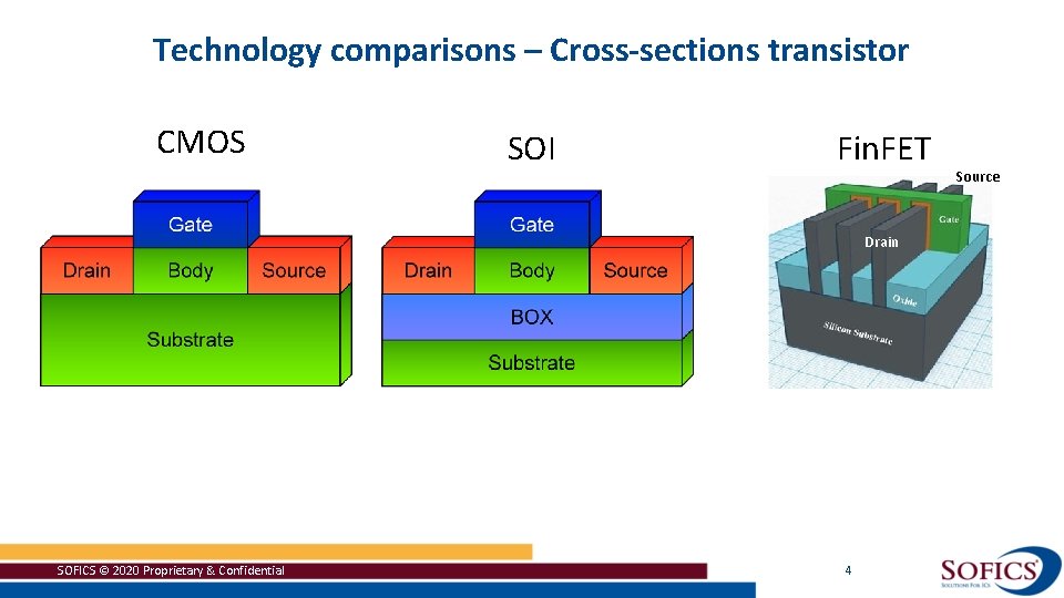
Technology comparisons – Cross-sections transistor CMOS SOI Fin. FET Drain SOFICS © 2020 Proprietary & Confidential 4 Source

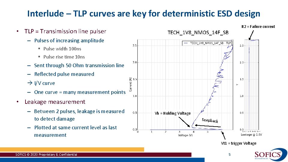
Interlude – TLP curves are key for deterministic ESD design It 2 = Failure current • TLP = Transimission line pulser – Pulses of increasing amplitude § Pulse width 100 ns § Pulse rise time 10 ns – Sent through 50 Ohm transmission line – Reflected pulse measured I/V curve – One curve = many measurement points • Leakage measurement – Between 2 pulses, leakage is measured to detect damage Vh = Holding Voltage Snapback – Plotted at same current level as last measurement Vt 1 = trigger Voltage SOFICS © 2020 Proprietary & Confidential 5

CMOS vs SOI vs Fin. FETs • Introduction • ESD Design Window – General Trend – LV NMOS comparison CMOS/SOI/Fin. FET – Technology options • ESD devices • Conclusion SOFICS © 2020 Proprietary & Confidential 6

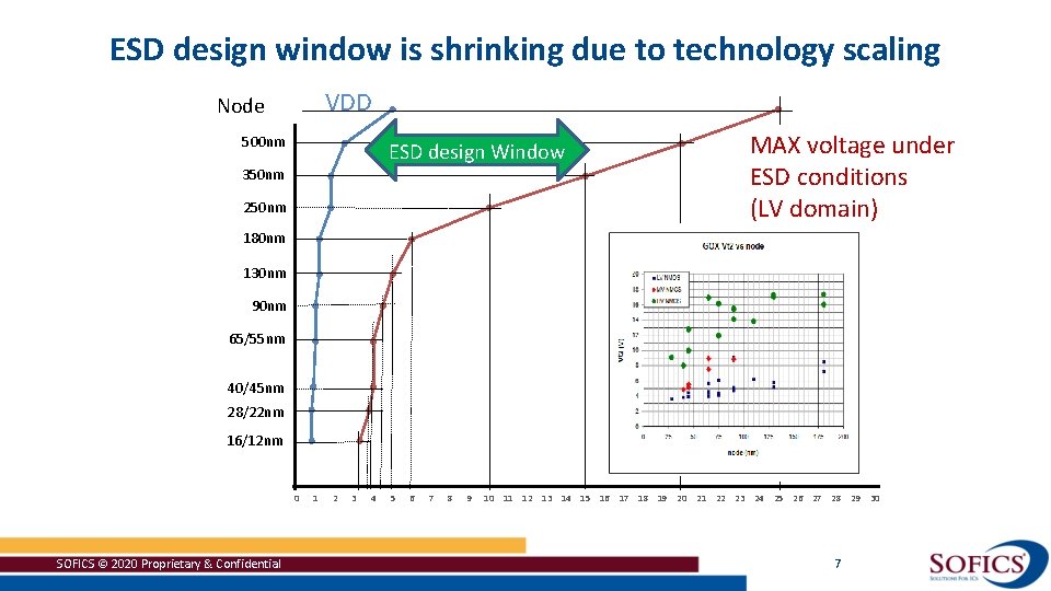
ESD design window is shrinking due to technology scaling VDD Node 500 nm ESD design Window 320 350 nm 250 nm 160 MAX voltage under ESD conditions (LV domain) 180 nm 130 nm 80 90 nm 65/55 nm 40 40/45 nm 28/22 nm 20 16/12 nm 25 V 10 SOFICS © 2020 Proprietary & Confidential 0 1 2 3 4 5 6 7 8 9 10 11 12 13 14 15 16 17 18 19 20 21 22 23 24 25 26 27 28 29 30 7

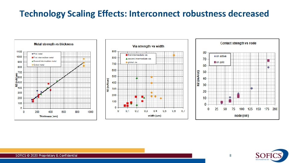
Technology Scaling Effects: Interconnect robustness decreased SOFICS © 2020 Proprietary & Confidential 8

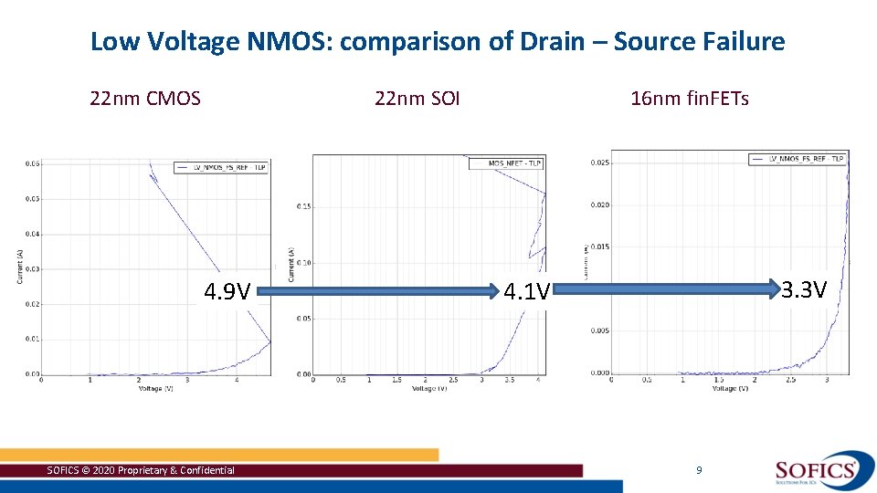
Low Voltage NMOS: comparison of Drain – Source Failure 22 nm CMOS 16 nm fin. FETs 22 nm SOI 4. 9 V SOFICS © 2020 Proprietary & Confidential 3. 3 V 4. 1 V 9

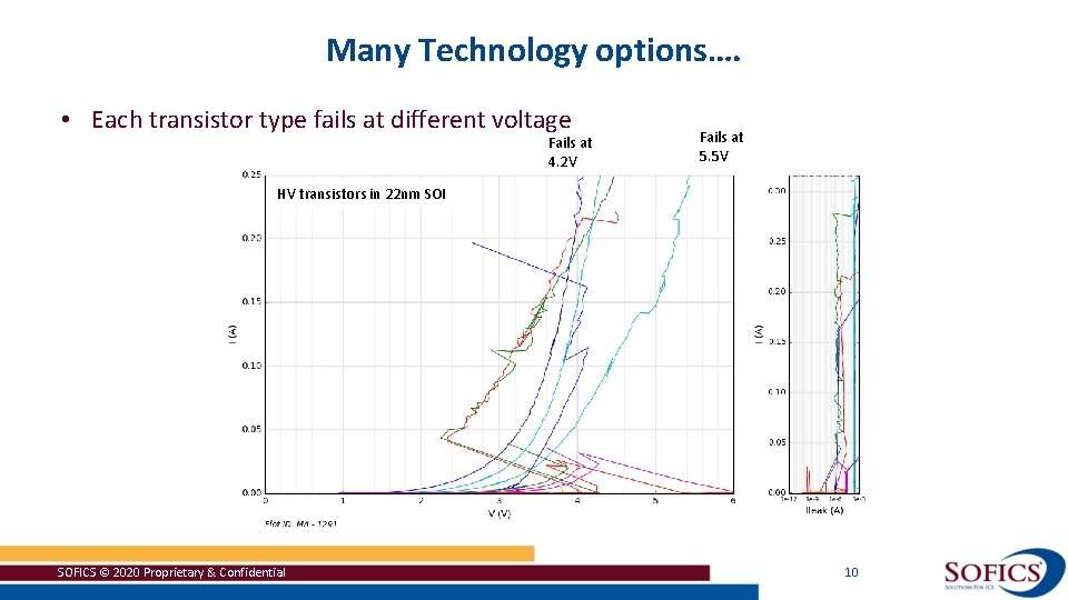
Many Technology options…. • Each transistor type fails at different voltage Fails at 4. 2 V Fails at 5. 5 V HV transistors in 22 nm SOI SOFICS © 2020 Proprietary & Confidential 10

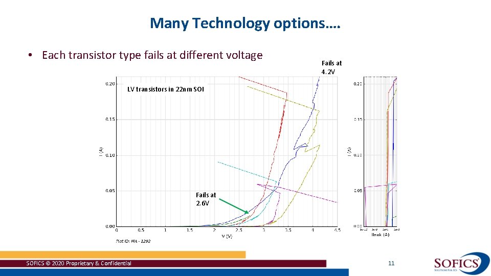
Many Technology options…. • Each transistor type fails at different voltage Fails at 4. 2 V LV transistors in 22 nm SOI Fails at 2. 6 V SOFICS © 2020 Proprietary & Confidential 11

CMOS vs SOI vs Fin. FETs • Introduction • ESD Design Window • ESD devices – ESD Strategy – Diodes – gg. NMOS – big. FET – SCR • Conclusion SOFICS © 2020 Proprietary & Confidential 12

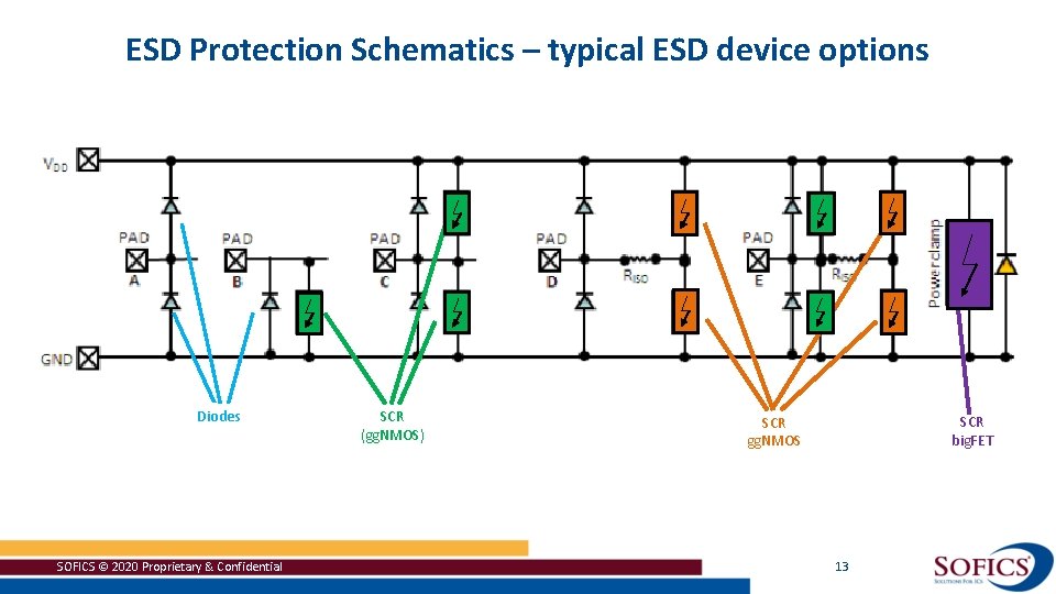
ESD Protection Schematics – typical ESD device options Diodes SOFICS © 2020 Proprietary & Confidential SCR (gg. NMOS) SCR big. FET SCR gg. NMOS 13

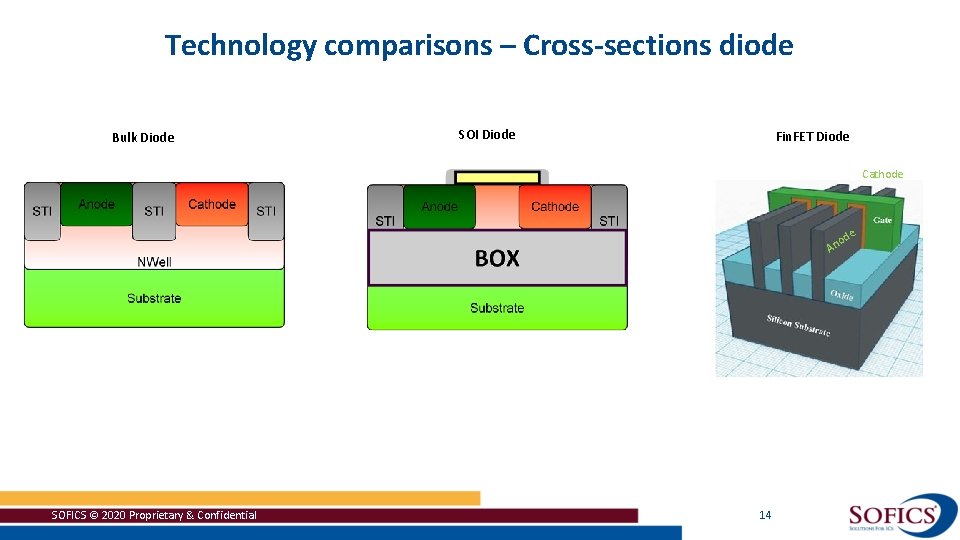
Technology comparisons – Cross-sections diode Bulk Diode SOI Diode Fin. FET Diode Cathode de o An SOFICS © 2020 Proprietary & Confidential 14

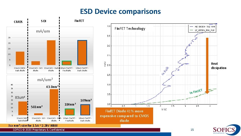
ESD Device comparisons Fin. FET SOI CMOS Fin. FET Technology m. A/um 25 20 15 10 5 16 nm Fin. FET Bulk Diode lk 22 nm SOI - SOI 22 nm SOI - Bulk 16 nm FIn. FET diode Fin diode In 22 nm CMOS Bulk diode Heat dissipation Bu 0 m. A/um² 40 43. 8 um² 35 FET In Fin 30 25 20 83 um² 15 581 um² 10 184 um² 109 um² 5 0 22 nm CMOS Bulk diode 22 nm SOI - SOI 22 nm SOI - Bulk 16 nm FIn. FET diode Fin diode 16 nm Fin. FET Bulk Diode Finf. ET Diode 41% more expensive compared to CMOS diode Xxx um²: size for 1. 5 A ~2. 2 k. V HBM SOFICS © 2020 Proprietary & Confidential 15

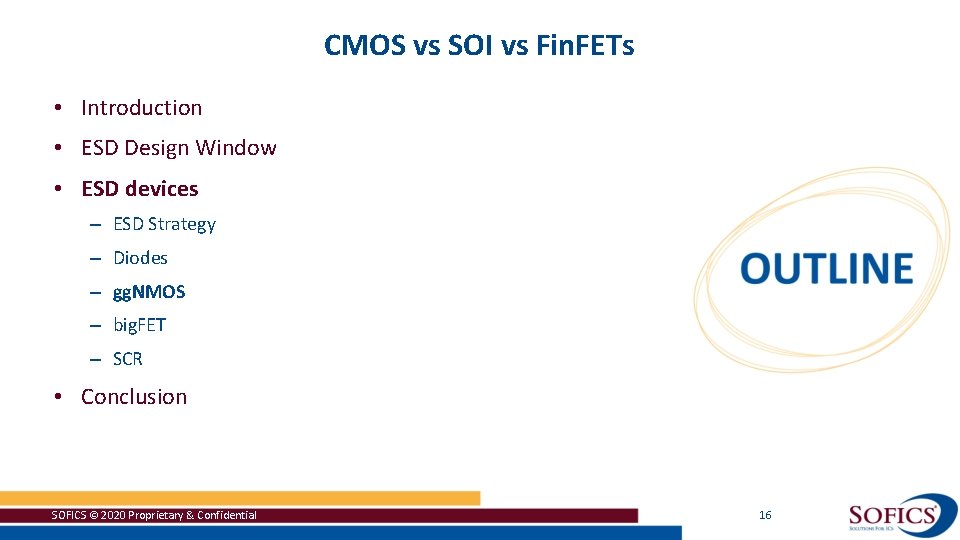
CMOS vs SOI vs Fin. FETs • Introduction • ESD Design Window • ESD devices – ESD Strategy – Diodes – gg. NMOS – big. FET – SCR • Conclusion SOFICS © 2020 Proprietary & Confidential 16

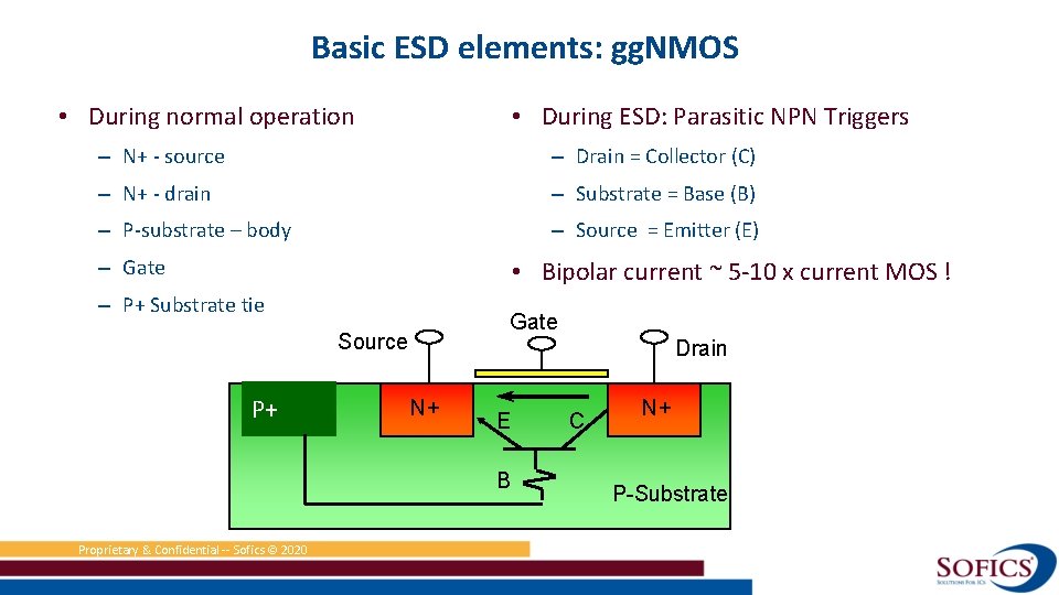
Basic ESD elements: gg. NMOS • During normal operation • During ESD: Parasitic NPN Triggers – N+ - source – Drain = Collector (C) – N+ - drain – Substrate = Base (B) – P-substrate – body – Source = Emitter (E) – Gate • Bipolar current ~ 5 -10 x current MOS ! – P+ Substrate tie Gate Source P+ Drain N+ E B Proprietary & Confidential -- Sofics © 2020 C N+ P-Substrate slide 17

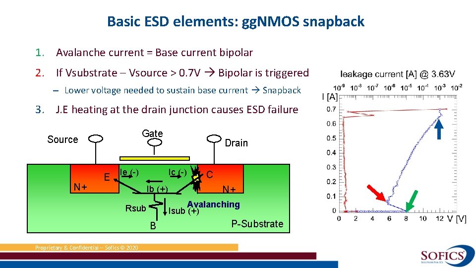
Basic ESD elements: gg. NMOS snapback 1. Avalanche current = Base current bipolar 2. If Vsubstrate – Vsource > 0. 7 V Bipolar is triggered – Lower voltage needed to sustain base current Snapback 3. J. E heating at the drain junction causes ESD failure Gate Source N+ E Ie (-) Ic (-) Ib (+) C N+ Avalanching Isub (+) Rsub B Proprietary & Confidential -- Sofics © 2020 Drain P-Substrate slide 18

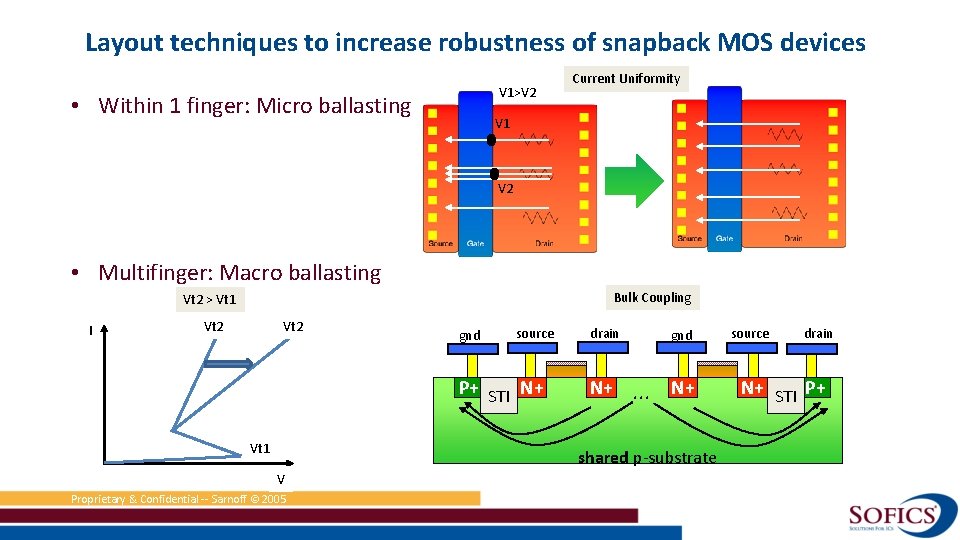
Layout techniques to increase robustness of snapback MOS devices V 1>V 2 • Within 1 finger: Micro ballasting Current Uniformity V 1 V 2 • Multifinger: Macro ballasting Bulk Coupling Vt 2 > Vt 1 I Vt 2 gnd source P+ STI N+ Vt 1 drain N+ gnd . . . N+ shared p-substrate V Proprietary & Confidential -- Sarnoff © 2005 slide 19 source drain N+ STI P+

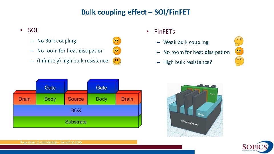
Bulk coupling effect – SOI/Fin. FET • SOI • Fin. FETs – No Bulk coupling – Weak bulk coupling – No room for heat dissipation – (Infinitely) high bulk resistance – High bulk resistance? Proprietary & Confidential -- Sarnoff © 2005 slide 20

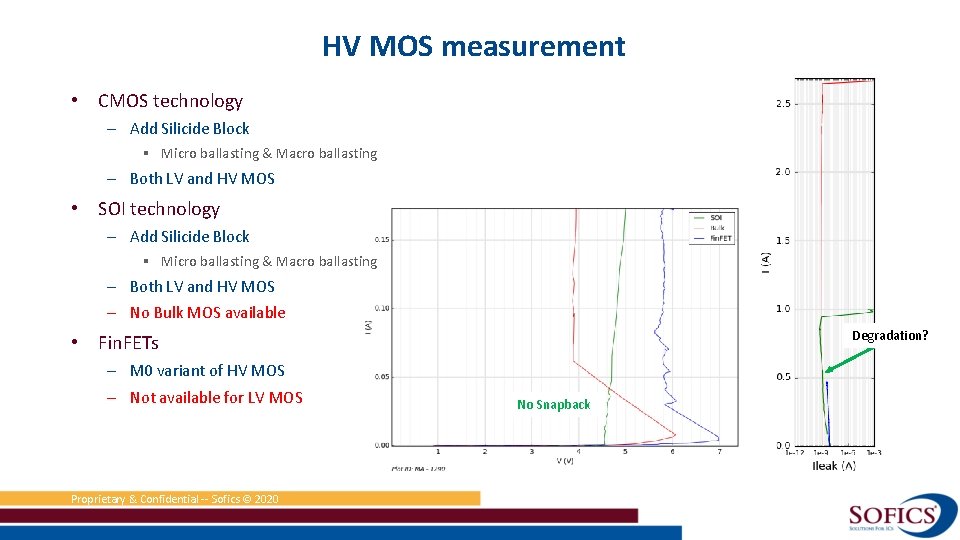
HV MOS measurement • CMOS technology – Add Silicide Block § Micro ballasting & Macro ballasting – Both LV and HV MOS • SOI technology – Add Silicide Block § Micro ballasting & Macro ballasting – Both LV and HV MOS – No Bulk MOS available Degradation? • Fin. FETs – M 0 variant of HV MOS – Not available for LV MOS Proprietary & Confidential -- Sofics © 2020 No Snapback slide 21

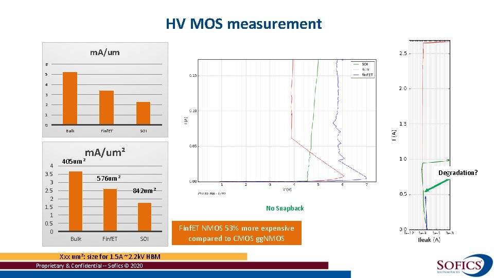
HV MOS measurement m. A/um 6 5 4 3 2 1 0 Bulk Finf. ET SOI m. A/um² 4 3. 5 3 2. 5 2 1. 5 1 0. 5 0 405 um² Degradation? 576 um² 842 um² No Snapback Bulk Finf. ET SOI Xxx um²: size for 1. 5 A ~2. 2 k. V HBM Proprietary & Confidential -- Sofics © 2020 Finf. ET NMOS 53% more expensive compared to CMOS gg. NMOS slide 22

CMOS vs SOI vs Fin. FETs • Introduction • ESD Design Window • ESD devices – ESD Strategy – Diodes – gg. NMOS – big. FET – SCR • Conclusion SOFICS © 2020 Proprietary & Confidential 23

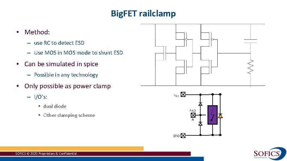
Big. FET railclamp • Method: – use RC to detect ESD – Use MOS in MOS mode to shunt ESD • Can be simulated in spice – Possible in any technology • Only possible as power clamp – I/O’s: § dual diode § Other clamping scheme SOFICS © 2020 Proprietary & Confidential

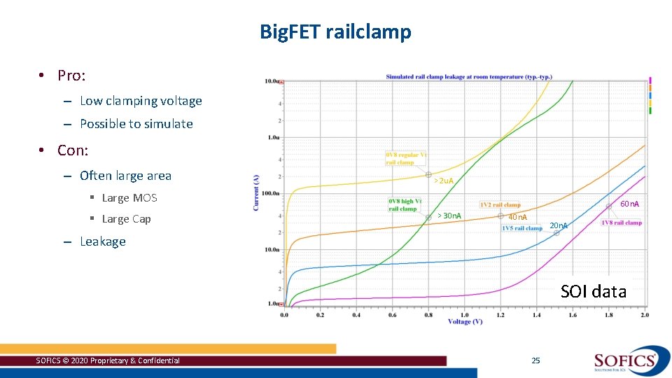
Big. FET railclamp • Pro: – Low clamping voltage – Possible to simulate • Con: – Often large area > 2 u. A § Large MOS § Large Cap 60 n. A > 30 n. A 40 n. A 20 n. A – Leakage SOI data SOFICS © 2020 Proprietary & Confidential 25

CMOS vs SOI vs Fin. FETs • Introduction • ESD Design Window • ESD devices – ESD Strategy – Diodes – gg. NMOS – big. FET – SCR • Conclusion SOFICS © 2020 Proprietary & Confidential 26

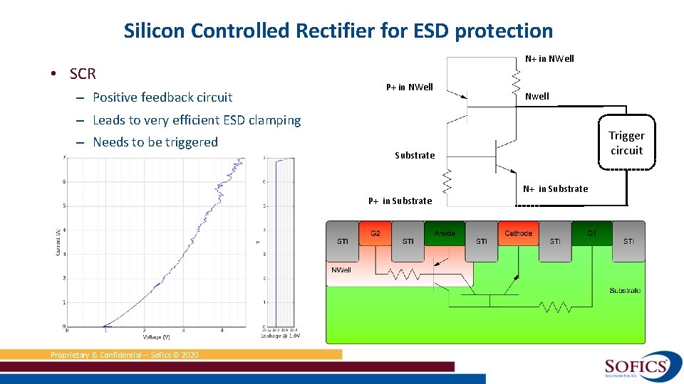
Silicon Controlled Rectifier for ESD protection • SCR – Positive feedback circuit N+ in NWell P+ in NWell Nwell – Leads to very efficient ESD clamping – Needs to be triggered Substrate P+ in Substrate Proprietary & Confidential -- Sofics © 2020 Trigger circuit slide 27 N+ in Substrate

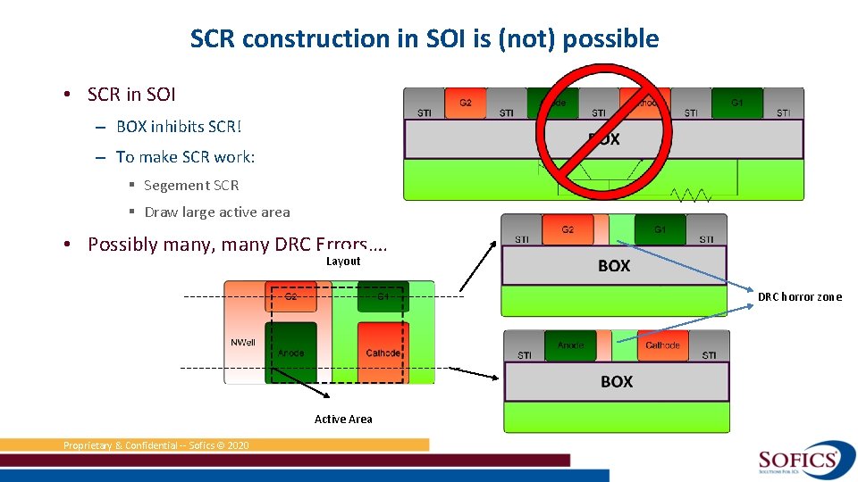
SCR construction in SOI is (not) possible • SCR in SOI – BOX inhibits SCR! – To make SCR work: § Segement SCR § Draw large active area • Possibly many, many DRC Errors…. Layout DRC horror zone Active Area Proprietary & Confidential -- Sofics © 2020 slide 28

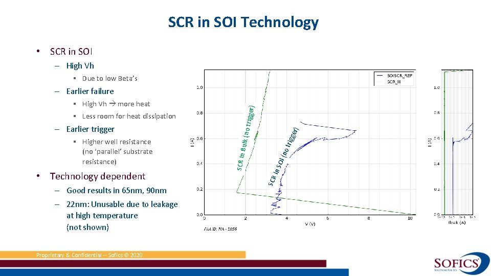
SCR in SOI Technology • SCR in SOI – High Vh § Due to low Beta’s • Technology dependent – Good results in 65 nm, 90 nm r) o tr igge OI ( n in S § Higher well resistance (no ‘parallel’ substrate resistance) SCR – Earlier trigger Bulk (n o § Less room for heat dissipation SCR in § High Vh more heat trigger ) – Earlier failure – 22 nm: Unusable due to leakage at high temperature (not shown) Proprietary & Confidential -- Sofics © 2020 slide 29

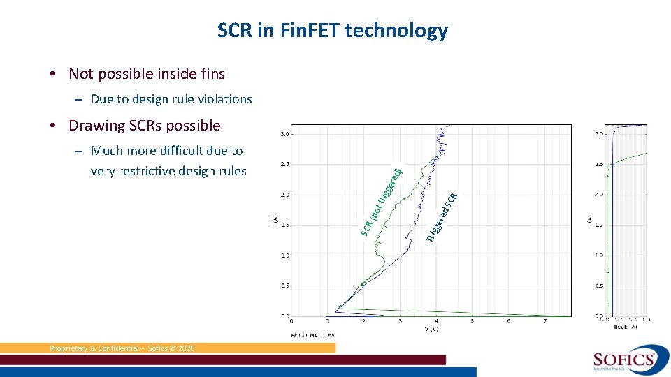
SCR in Fin. FET technology • Not possible inside fins – Due to design rule violations • Drawing SCRs possible Proprietary & Confidential -- Sofics © 2020 red gge Tri SCR (no t tr SCR igg ere d) – Much more difficult due to very restrictive design rules slide 30

Conclusion • Vulnerable technologies – CMOS > SOI > Fin. FET • Need for ‘bulk’ devices – Available in some SOI technologies – Available in fin. FET technology • Cost! – Wafer price: 8% different – ESD cost per device: upto 50% difference – Only based on failure current § On Resistance, small design window, …. Can make it worse Proprietary & Confidential -- Sofics © 2020 slide 31

Contact us • Sofics contact Benjamin Van Camp bvancamp@sofics. com SOFICS bv Sint-Godelievestraat 32 9880 Aalter, Belgium SOFICS © 2020 Proprietary & Confidential 32