
TWEPP 2019 Topical Workshop on Electronics for Particle

- Slides: 23
TWEPP 2019 Topical Workshop on Electronics for Particle Physics Highly-linear FPGA-based Data Acquisition System for Multi-channel Si. PM Readout Todd Townsend, Yuxuan Tang, Jinghong Chen Department of Electrical and Computer Engineering, University of Houston, TX 77204 September 5, 2019
Outline • • Motivation Si. PM FPGA DAQ Architecture Detection Pulse Energy TDC Results Summary 2
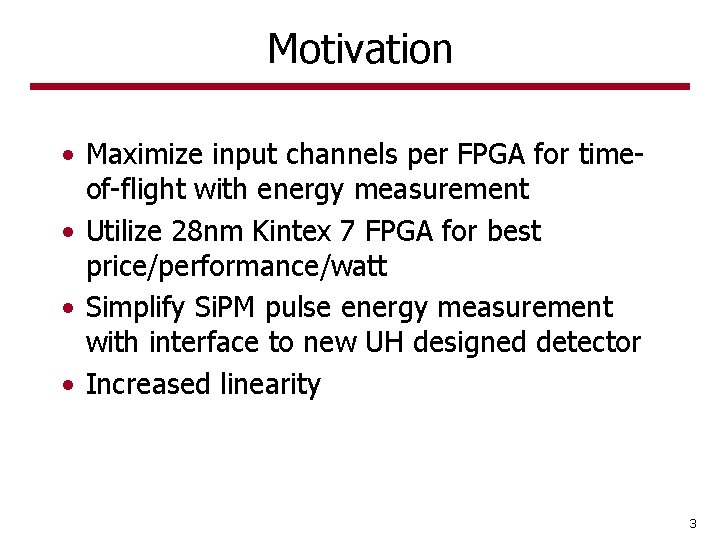
Motivation • Maximize input channels per FPGA for timeof-flight with energy measurement • Utilize 28 nm Kintex 7 FPGA for best price/performance/watt • Simplify Si. PM pulse energy measurement with interface to new UH designed detector • Increased linearity 3
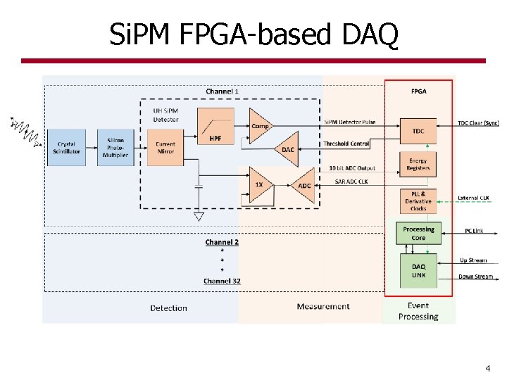
Si. PM FPGA-based DAQ 4
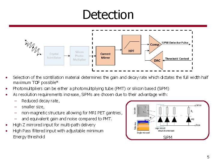
Detection • • • Selection of the scintillation material determines the gain and decay rate which dictates the full width half maximum TOF possible* Photomultipliers can be either a photomultiplying tube (PMT) or silicon based (Si. PM) As resolution requirements increase, Si. PMs are chosen due to their advantage with: Reduced decay rate, smaller size, non-magnetic structure allowing for MRI PET gantries, and equivalent gain and noise compared to PMT. High Z mirrored input for multi-path delivery High Pass filtered input with adjustable minimum Energy threshold Si. PM 5
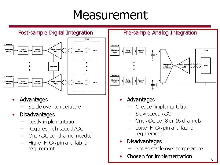
Measurement Post-sample Digital Integration • Advantages Pre-sample Analog Integration • Advantages Stable over temperature Cheaper implementation Slow-speed ADC One ADC per 8 or 16 channels Lower FPGA pin and fabric requirement • Disadvantages Costly implementation Requires high-speed ADC One ADC per channel needed Higher FPGA pin and fabric requirement • Disadvantages Not as stable over temperature • Chosen for implementation 6
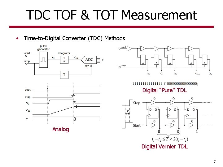
TDC TOF & TOT Measurement • Time-to-Digital Converter (TDC) Methods Digital “Pure” TDL Analog Digital Vernier TDL 7
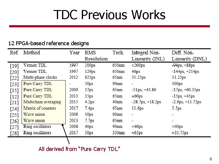
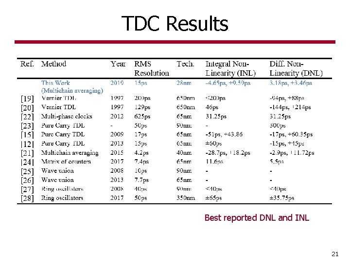
TDC Previous Works 12 FPGA-based reference designs All derived from “Pure Carry TDL” 8
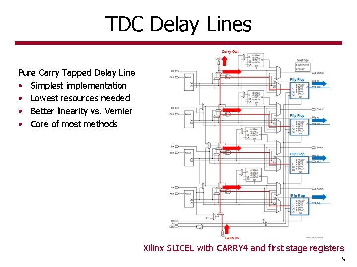
TDC Delay Lines Pure Carry Tapped Delay Line • Simplest implementation • Lowest resources needed • Better linearity vs. Vernier • Core of most methods Xilinx SLICEL with CARRY 4 and first stage registers 9
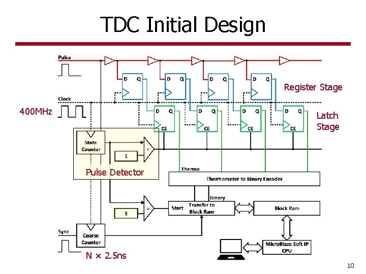
TDC Initial Design Register Stage 400 MHz Latch Stage Pulse Detector N × 2. 5 ns 10
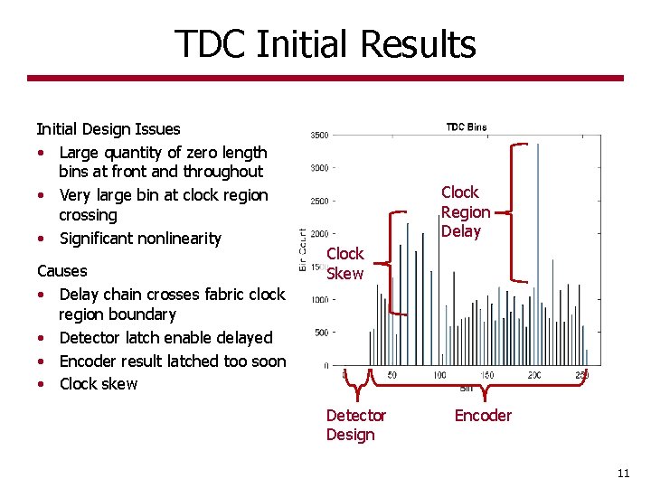
TDC Initial Results Initial Design Issues • Large quantity of zero length bins at front and throughout • Very large bin at clock region crossing • Significant nonlinearity Causes • Delay chain crosses fabric clock region boundary • Detector latch enable delayed • Encoder result latched too soon • Clock skew Clock Region Delay Clock Skew Detector Design Encoder 11
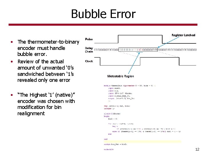
Bubble Error • The thermometer-to-binary encoder must handle bubble error. • Review of the actual amount of unwanted ‘ 0’s sandwiched between ‘ 1’s revealed only one error • “The Highest ‘ 1’ (native)” encoder was chosen with modification for bin realignment 12
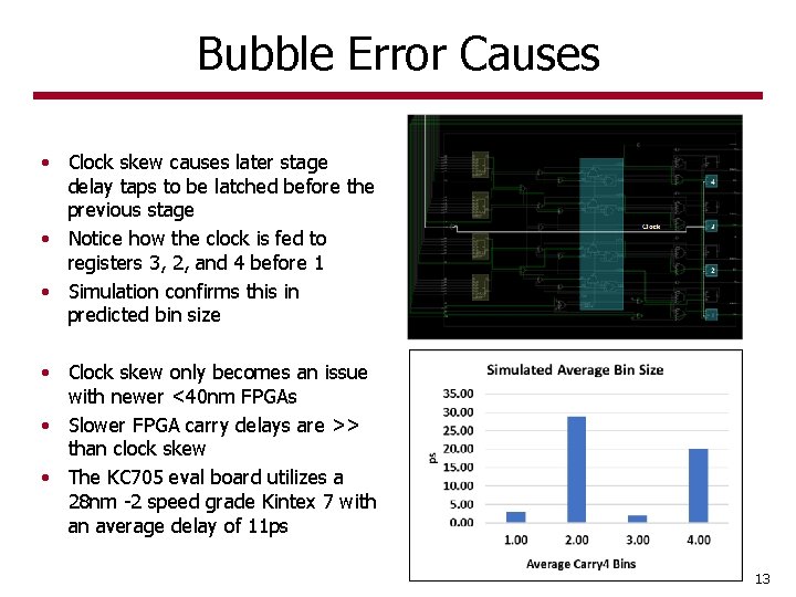
Bubble Error Causes • Clock skew causes later stage delay taps to be latched before the previous stage • Notice how the clock is fed to registers 3, 2, and 4 before 1 • Simulation confirms this in predicted bin size • Clock skew only becomes an issue with newer <40 nm FPGAs • Slower FPGA carry delays are >> than clock skew • The KC 705 eval board utilizes a 28 nm -2 speed grade Kintex 7 with an average delay of 11 ps 13
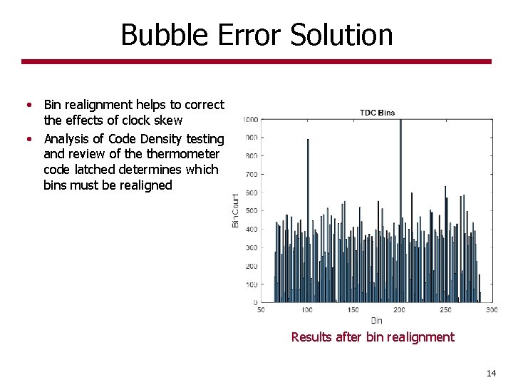
Bubble Error Solution • Bin realignment helps to correct the effects of clock skew • Analysis of Code Density testing and review of thermometer code latched determines which bins must be realigned Results after bin realignment 14
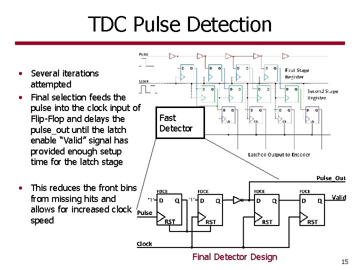
TDC Pulse Detection • Several iterations attempted • Final selection feeds the pulse into the clock input of Flip-Flop and delays the pulse_out until the latch enable “Valid” signal has provided enough setup time for the latch stage Fast Detector • This reduces the front bins from missing hits and allows for increased clock speed Final Detector Design 15
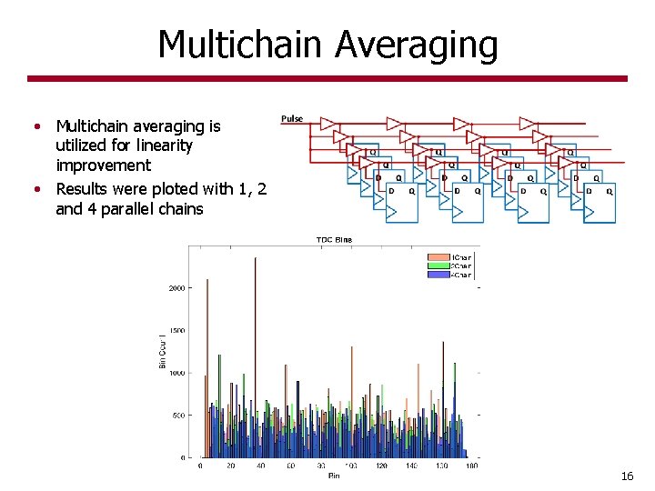
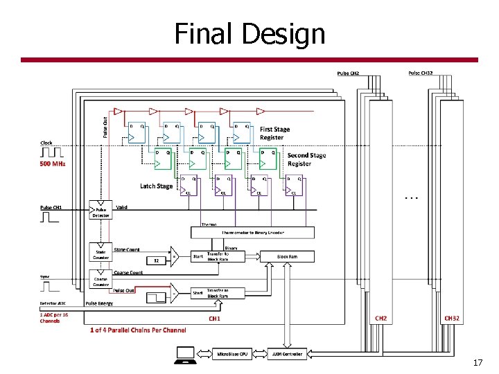
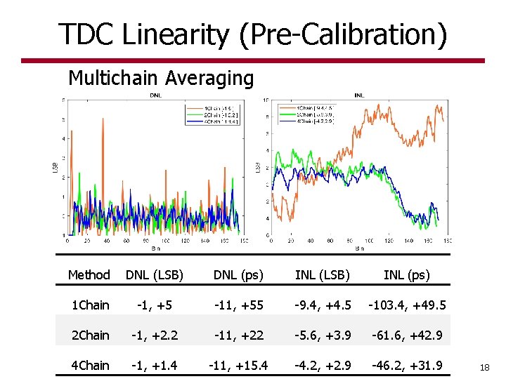
Multichain Averaging • Multichain averaging is utilized for linearity improvement • Results were ploted with 1, 2 and 4 parallel chains 16
Final Design 17
TDC Linearity (Pre-Calibration) Multichain Averaging Method DNL (LSB) DNL (ps) INL (LSB) INL (ps) 1 Chain -1, +5 -11, +55 -9. 4, +4. 5 -103. 4, +49. 5 2 Chain -1, +2. 2 -11, +22 -5. 6, +3. 9 -61. 6, +42. 9 4 Chain -1, +1. 4 -11, +15. 4 -4. 2, +2. 9 -46. 2, +31. 9 18
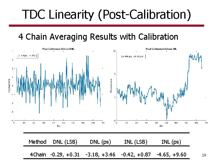
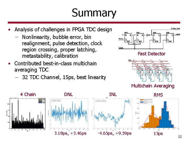
TDC Linearity (Post-Calibration) 4 Chain Averaging Results with Calibration Method DNL (LSB) 4 Chain -0. 29, +0. 31 DNL (ps) INL (LSB) INL (ps) -3. 18, +3. 46 -0. 42, +0. 87 -4. 65, +9. 60 19
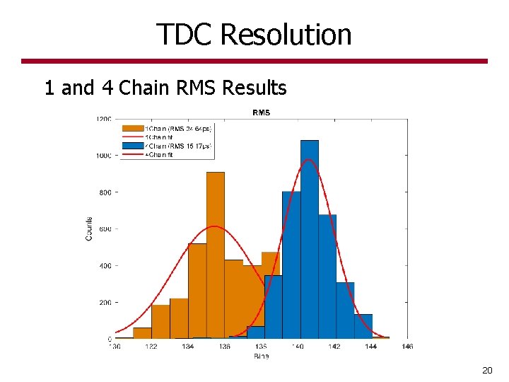
TDC Resolution 1 and 4 Chain RMS Results 20
TDC Results Best reported DNL and INL 21
Summary • Analysis of challenges in FPGA TDC design Nonlinearity, bubble error, bin realignment, pulse detection, clock region crossing, proper latching, metastability, calibration • Contributed best-in-class multichain averaging TDC 32 TDC Channel, 15 ps, best linearity Fast Detector Multichain Averaging 4 Chain DNL 3. 18 ps, +3. 46 ps INL -4. 65 ps, +9. 59 ps RMS 15 ps 22
Thank you for your attention! Q&A 23