
Silicon On Insulator Technology NanoMOSFETs with Giga Effects







- Slides: 67
Silicon On Insulator Technology: Nano-MOSFETs with Giga Effects Sorin Cristoloveanu - Short introduction to warm up - Self-heating & Novel SOI materials - Gate tunneling and new floating-body effects - Fringing fields, short-channel effects and scaling - Narrow-channel effects - Extremely thin film effects - Double-gate operation - Fin. FETs and Triple-gate MOSFETs - Four-Gate transistor - Next speaker
SOI Technology - Definition & Questions Definition: SOI is a young technology for the future of the microelectronics Questions: • Is SOI really young ? • Is SOI for the future ? • Is the future what it used to be ? Free answers available during lunch … Sorin 20 -05
MOSFET Scaling - Concerns Roadmap Traffic Lights Sorin 30 -01
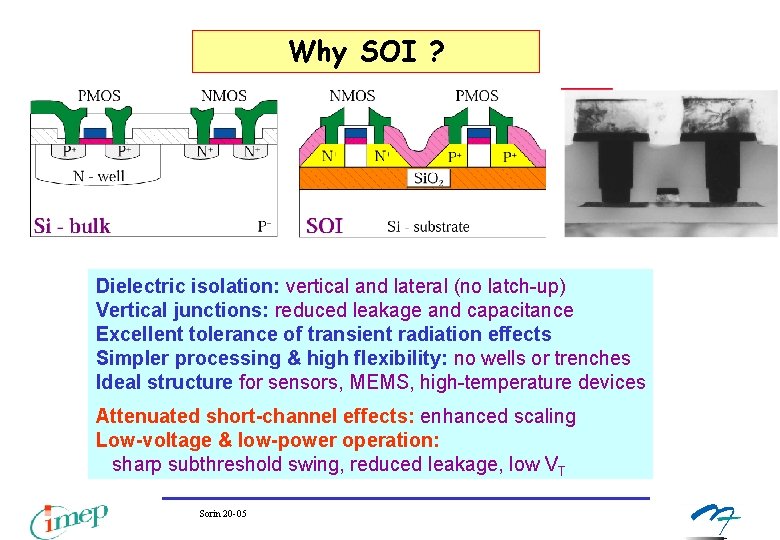
Why SOI ? Dielectric isolation: vertical and lateral (no latch-up) Vertical junctions: reduced leakage and capacitance Excellent tolerance of transient radiation effects Simpler processing & high flexibility: no wells or trenches Ideal structure for sensors, MEMS, high-temperature devices Attenuated short-channel effects: enhanced scaling Low-voltage & low-power operation: sharp subthreshold swing, reduced leakage, low VT Sorin 20 -05
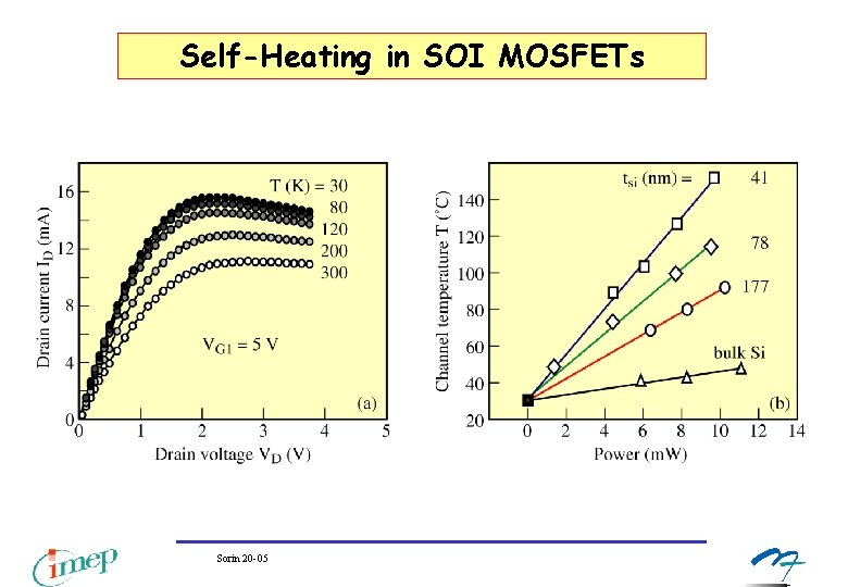
Self-Heating in SOI MOSFETs Sorin 20 -05
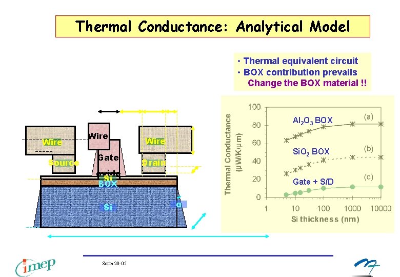
Thermal Conductance: Analytical Model • Thermal equivalent circuit • BOX contribution prevails Change the BOX material !! Al 2 O 3 BOX Wire Source Wire Gate oxide Si BOX Si Sorin 20 -05 Wire Si. O 2 BOX Drain Gate + S/D α
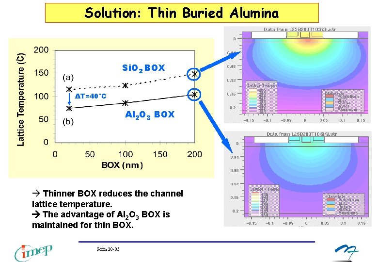
Solution: Thin Buried Alumina o Si. O 2 BOX ΔT=40°C Al 2 O 3 BOX à Thinner BOX reduces the channel lattice temperature. The advantage of Al 2 O 3 BOX is maintained for thin BOX. Sorin 20 -05
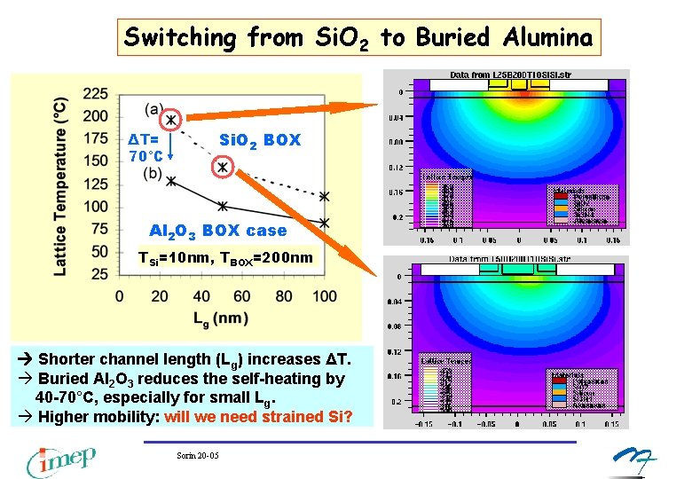
Switching from Si. O 2 to Buried Alumina o Si. O 2 BOX ΔT= 70°C Al 2 O 3 BOX case TSi=10 nm, TBOX=200 nm Shorter channel length (Lg) increases ΔT. à Buried Al 2 O 3 reduces the self-heating by 40 -70°C, especially for small Lg. à Higher mobility: will we need strained Si? Sorin 20 -05
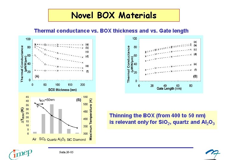
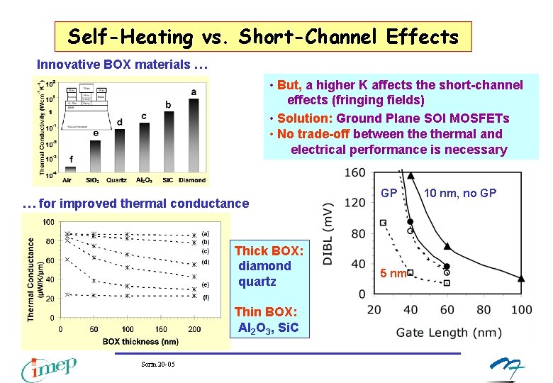
Novel BOX Materials Thermal conductance vs. BOX thickness and vs. Gate length Thinning the BOX (from 400 to 50 nm) is relevant only for Si. O 2, quartz and Al 2 O 3 Sorin 20 -05
Self-Heating vs. Short-Channel Effects Innovative BOX materials … • But, a higher K affects the short-channel effects (fringing fields) • Solution: Ground Plane SOI MOSFETs • No trade-off between thermal and electrical performance is necessary … for improved thermal conductance Thick BOX: diamond quartz Thin BOX: Al 2 O 3, Si. C Sorin 20 -05 GP 5 nm 10 nm, no GP
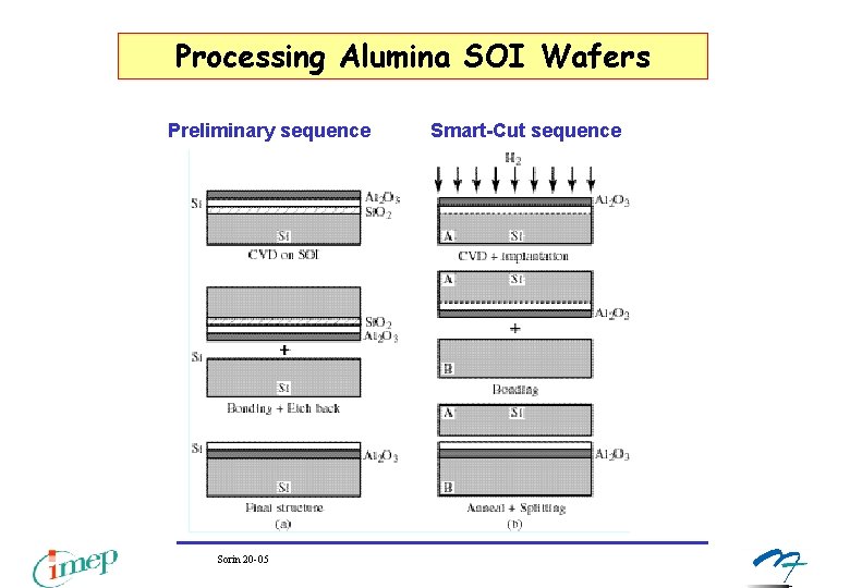
Processing Alumina SOI Wafers Preliminary sequence Smart-Cut sequence Sorin 20 -05
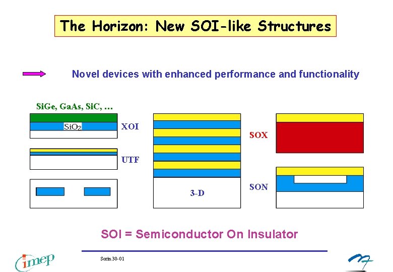
The Horizon: New SOI-like Structures Novel devices with enhanced performance and functionality Si. Ge, Ga. As, Si. C, … XOI SOX UTF 3 -D SON SOI = Semiconductor On Insulator Sorin 30 -01
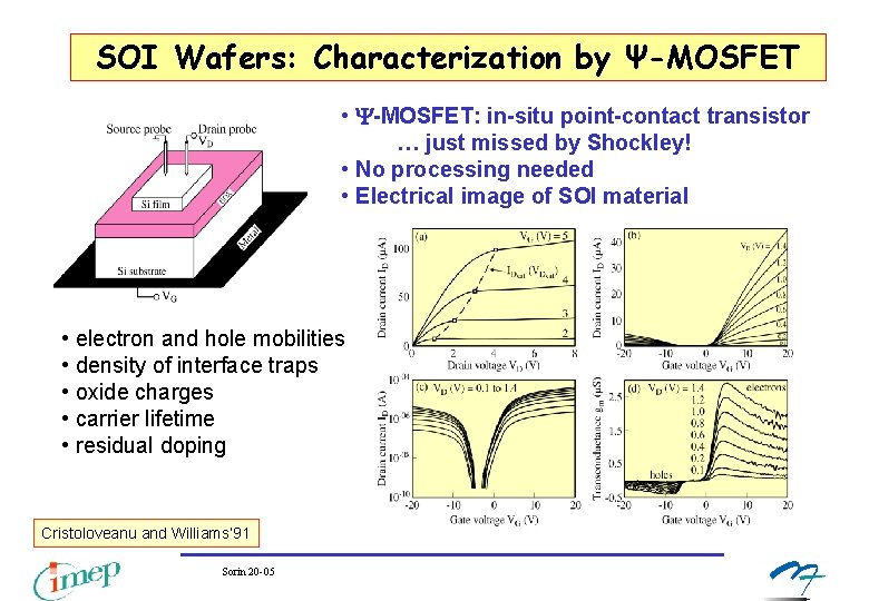
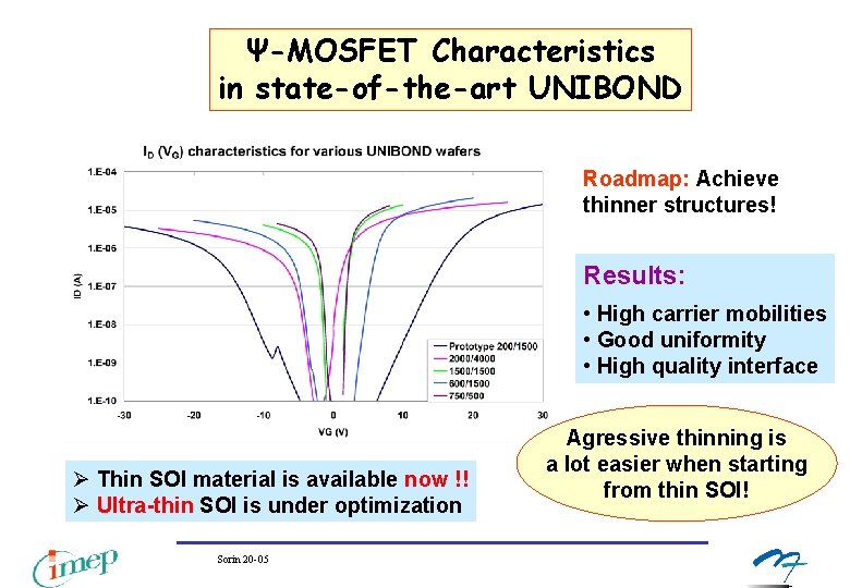
SOI Wafers: Characterization by Ψ-MOSFET • -MOSFET: in-situ point-contact transistor … just missed by Shockley! • No processing needed • Electrical image of SOI material • electron and hole mobilities • density of interface traps • oxide charges • carrier lifetime • residual doping Cristoloveanu and Williams’ 91 Sorin 20 -05
Ψ-MOSFET Characteristics in state-of-the-art UNIBOND Roadmap: Achieve thinner structures! Results: • High carrier mobilities • Good uniformity • High quality interface Ø Thin SOI material is available now !! Ø Ultra-thin SOI is under optimization Sorin 20 -05 Agressive thinning is a lot easier when starting from thin SOI!
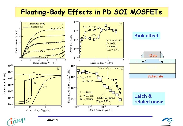
Floating-Body Effects in PD SOI MOSFETs Kink effect Gate S BOX Substrate Latch & related noise Sorin 20 -05 D
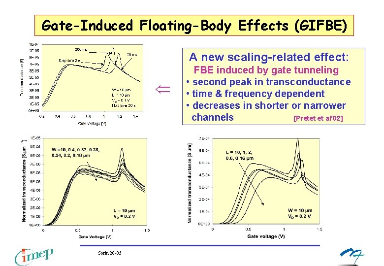
Gate-Induced Floating-Body Effects (GIFBE) A new scaling-related effect: Sorin 20 -05 FBE induced by gate tunneling • second peak in transconductance • time & frequency dependent • decreases in shorter or narrower channels [Pretet et al’ 02]
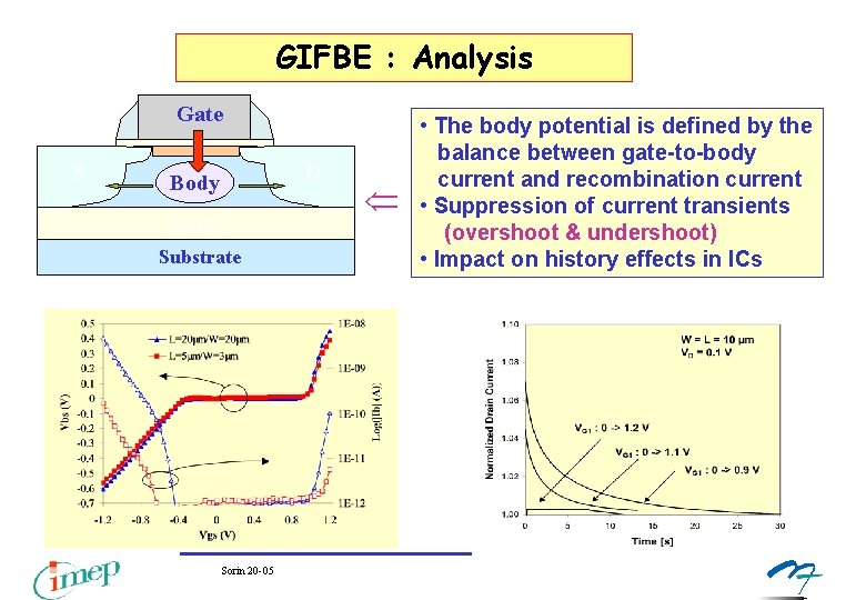
GIFBE : Analysis Gate S D Body BOX Substrate Sorin 20 -05 • The body potential is defined by the balance between gate-to-body current and recombination current • Suppression of current transients (overshoot & undershoot) • Impact on history effects in ICs
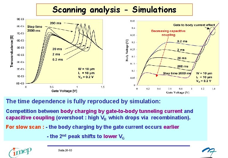
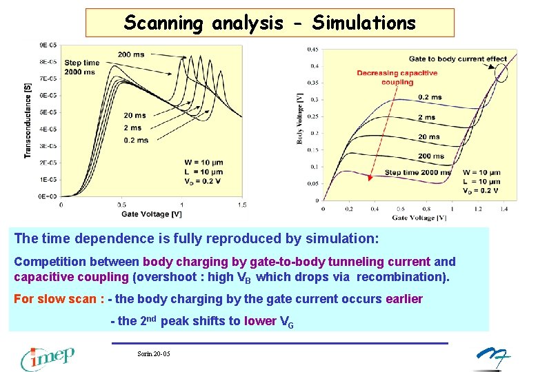
Scanning analysis - Simulations The time dependence is fully reproduced by simulation: Competition between body charging by gate-to-body tunneling current and capacitive coupling (overshoot : high VB which drops via recombination). For slow scan : - the body charging by the gate current occurs earlier - the 2 nd peak shifts to lower VG Sorin 20 -05
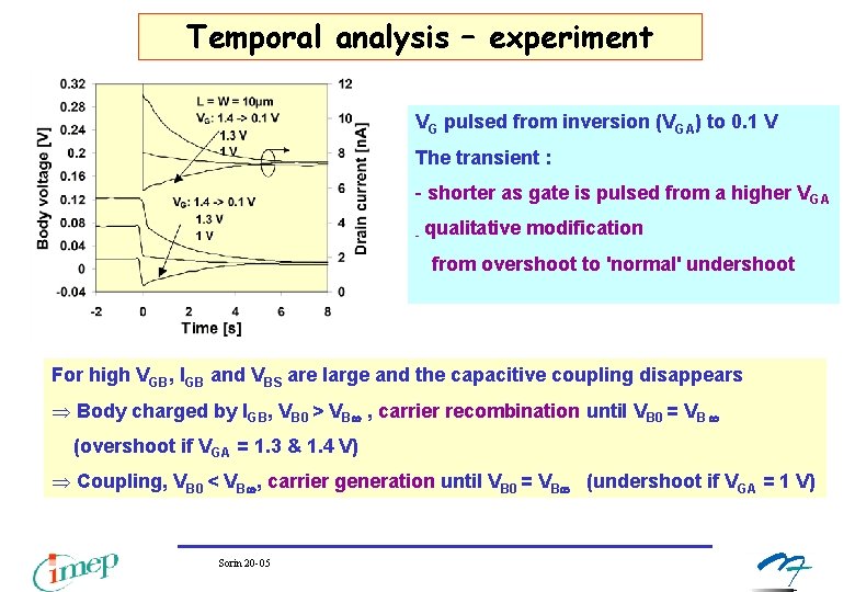
Temporal analysis – experiment VG pulsed from inversion (VGA) to 0. 1 V The transient : - shorter as gate is pulsed from a higher VGA - qualitative modification from overshoot to 'normal' undershoot For high VGB, IGB and VBS are large and the capacitive coupling disappears Þ Body charged by IGB, VB 0 > VB , carrier recombination until VB 0 = VB (overshoot if VGA = 1. 3 & 1. 4 V) Þ Coupling, VB 0 < VB , carrier generation until VB 0 = VB (undershoot if VGA = 1 V) Sorin 20 -05
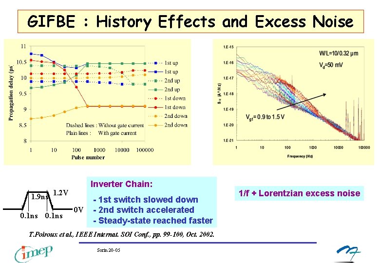
GIFBE : History Effects and Excess Noise 1. 9 ns 1. 2 V 0. 1 ns Inverter Chain: - 1 st switch slowed down 0 V - 2 nd switch accelerated - Steady-state reached faster T. Poiroux et al. , IEEE Internat. SOI Conf. , pp. 99 -100, Oct. 2002. Sorin 20 -05 1/f + Lorentzian excess noise
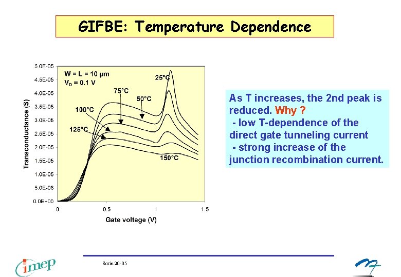
GIFBE: Temperature Dependence As T increases, the 2 nd peak is reduced. Why ? - low T-dependence of the direct gate tunneling current - strong increase of the junction recombination current. Sorin 20 -05
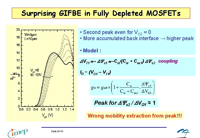
Surprising GIFBE in Fully Depleted MOSFETs • Second peak even for VG 2 = 0 • More accumulated back interface → higher peak • Model : VT 1 - s 1 -Csi/(Csi + Cox 1) s 2 coupling ID ~ (VG 1 – VT 1) Peak for s 2 / VG 1 ≈ 1 Wrong mobility extraction from peak!!! Sorin 20 -05
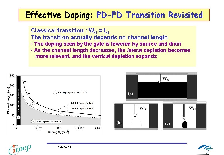
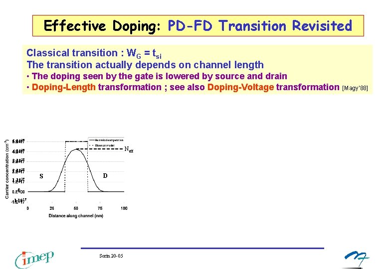
Effective Doping: PD-FD Transition Revisited Classical transition : WG = tsi The transition actually depends on channel length • The doping seen by the gate is lowered by source and drain • As the channel length decreases, the lateral depletion becomes more relevant, and the vertical depletion expands Sorin 20 -05
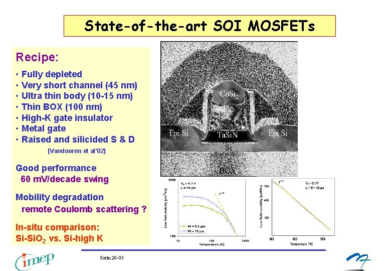
State-of-the-art SOI MOSFETs Recipe: • Fully depleted • Very short channel (45 nm) • Ultra thin body (10 -15 nm) • Thin BOX (100 nm) • High-K gate insulator • Metal gate • Raised and silicided S & D [Vandooren et al’ 02] Good performance 60 m. V/decade swing Mobility degradation remote Coulomb scattering ? In-situ comparison: Si-Si. O 2 vs. Si-high K Sorin 20 -05
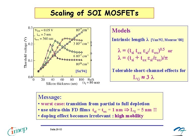
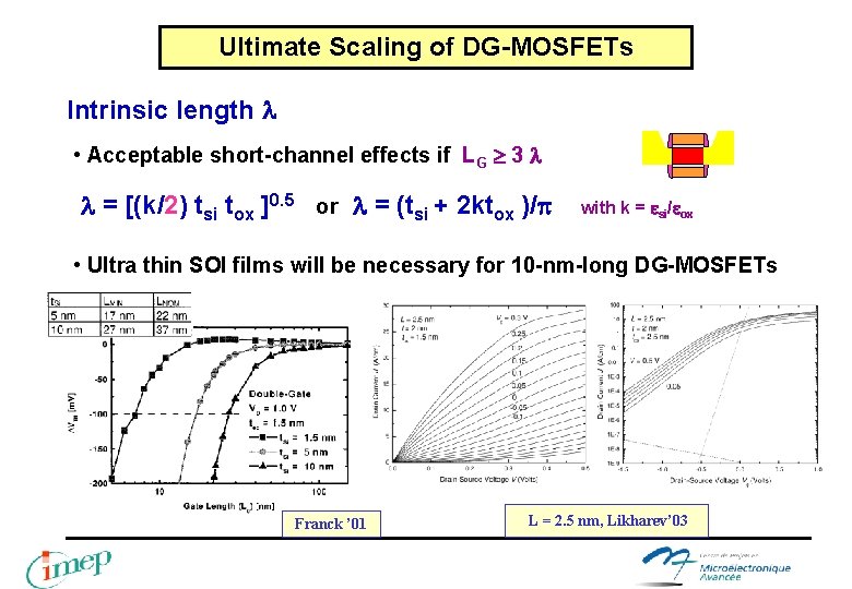
Scaling of SOI MOSFETs Models Intrinsic length λ [Yan’ 92, Monroe ’ 00] λ = (tsi tox εsi/ εox)0. 5 or λ = (tsi + tox εsi/εox)/π [Su’ 94] Tolerable short-channel effects for LG 3 λ Message: • worst case: transition from partial to full depletion • use ultra-thin FD films tsi = tox = 1 nm LG = 5 nm !! • doping effect becomes irrelevant : high mobility Sorin 20 -05
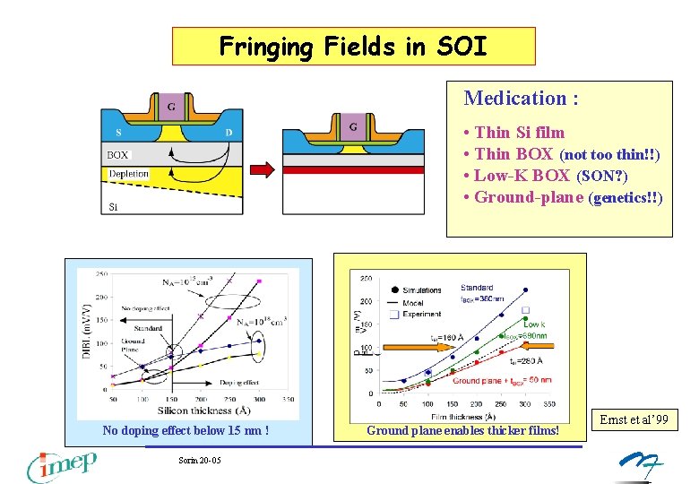
Fringing Fields in SOI Medication : • Thin Si film • Thin BOX (not too thin!!) • Low-K BOX (SON? ) • Ground-plane (genetics!!) No doping effect below 15 nm ! Sorin 20 -05 Ground plane enables thicker films! Ernst et al’ 99
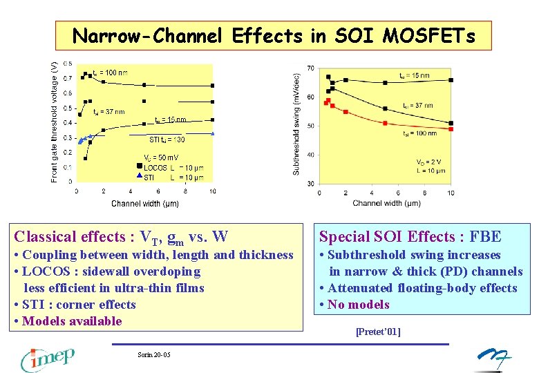
Narrow-Channel Effects in SOI MOSFETs Classical effects : VT, gm vs. W • Coupling between width, length and thickness • LOCOS : sidewall overdoping less efficient in ultra-thin films • STI : corner effects • Models available Sorin 20 -05 Special SOI Effects : FBE • Subthreshold swing increases in narrow & thick (PD) channels • Attenuated floating-body effects • No models [Pretet’ 01]
Floating-Body Effects in Narrow SOI MOSFETs • Breakdown and snapback voltages increase in narrow channels • Transients effects are much shorter • Reduced history effects [Pretet’ 01] Sorin 20 -05 Why are FBE attenuated ? • Degraded carrier lifetime on the sidewalls - stress-induced defects ? • Dopant out-diffusion & segregation into the lateral isolation oxide - reduced doping, lower S-body barrier - enhanced junction leakage current
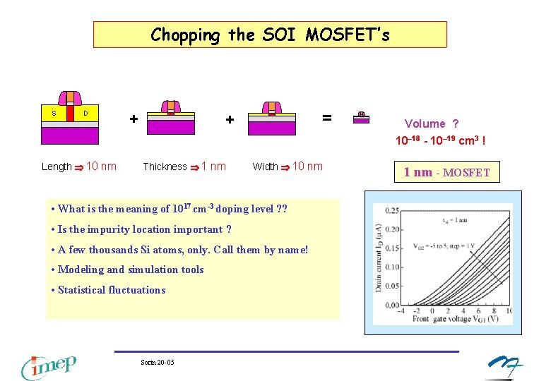
Chopping the SOI MOSFET’s S D + = + Volume ? 10– 18 - 10– 19 cm 3 ! Length 10 nm Thickness 1 nm Width 10 nm • What is the meaning of 1017 cm-3 doping level ? ? • Is the impurity location important ? • A few thousands Si atoms, only. Call them by name! • Modeling and simulation tools • Statistical fluctuations Sorin 20 -05 1 nm - MOSFET
Ultimate Scaling of DG-MOSFETs Intrinsic length • Acceptable short-channel effects if LG 3 = [(k/2) tsi tox ]0. 5 or = (tsi + 2 ktox )/ with k = si/ ox • Ultra thin SOI films will be necessary for 10 -nm-long DG-MOSFETs Franck ’ 01 L = 2. 5 nm, Likharev’ 03
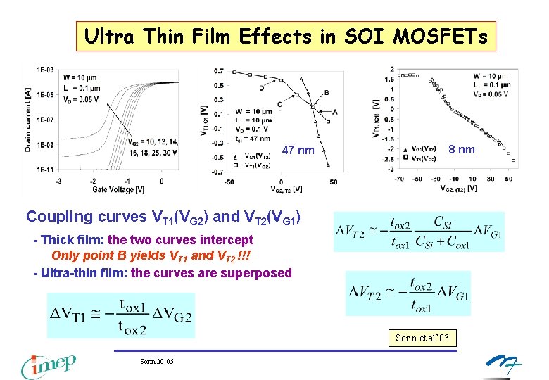
Ultra Thin Film Effects in SOI MOSFETs 47 nm 8 nm Coupling curves VT 1(VG 2) and VT 2(VG 1) - Thick film: the two curves intercept Only point B yields VT 1 and VT 2 !!! - Ultra-thin film: the curves are superposed Sorin et al’ 03 Sorin 20 -05
SOI Dictionary Super-coupling effect Sorin 20 -05
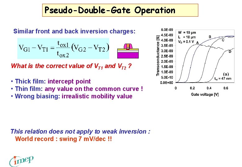
Pseudo-Double-Gate Operation Similar front and back inversion charges: What is the correct value of VT 1 and VT 2 ? • Thick film: intercept point • Thin film: any value on the common curve ! • Wrong biasing: irrealistic mobility value This relation does not apply to weak inversion : World record : swing 7 m. V/dec !!
Ultimately Thin Double-Gate MOSFETs • 3 -nm-thick DG-MOSFET • simultaneous biasing of front and back gates: VG 2 = 1. 2 VG 1 • outstanding transconductance gain: up to 400% • mobility effect rather than charge effect Impact of volume inversion Cristoloveanu et al’ 99 Sorin 20 -05
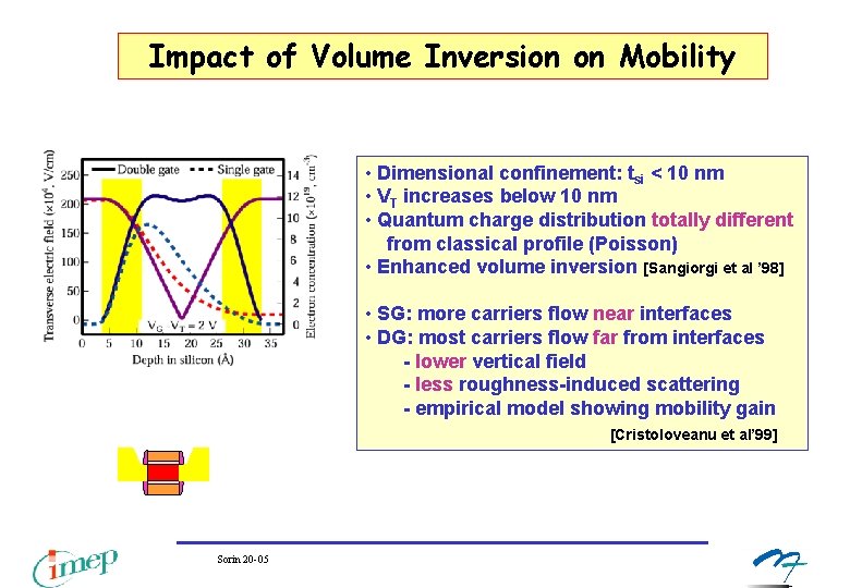
Impact of Volume Inversion on Mobility • Dimensional confinement: tsi < 10 nm • VT increases below 10 nm • Quantum charge distribution totally different from classical profile (Poisson) • Enhanced volume inversion [Sangiorgi et al ’ 98] • SG: more carriers flow near interfaces • DG: most carriers flow far from interfaces - lower vertical field - less roughness-induced scattering - empirical model showing mobility gain [Cristoloveanu et al’ 99] Sorin 20 -05
Carrier Mobility in Ultra Thin SOI MOSFETs • Monte-Carlo simulations indicate [Gamiz’ 01] : (including phonon + Coulomb + surface roughness scattering) - enhanced mobility in sub-10 -nm thickness range - higher mobility in DG-MOSFETs • Experiments in MOS-Hall devices demonstrate [Mastrapasqua’ 01] : - impoved mobility in recent SOI materials - good mobility in sub-10 -nm thick MOSFETs Compact models ? ? - higher mobility in DG-MOSFETs
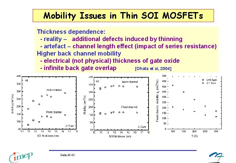
Mobility Issues in Thin SOI MOSFETs Thickness dependence: - reality – additional defects induced by thinning - artefact – channel length effect (impact of series resistance) Higher back channel mobility - electrical (not physical) thickness of gate oxide - infinite back gate overlap [Ohata et al, 2004] Sorin 20 -05
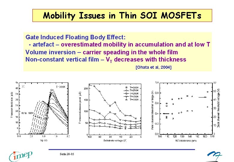
Mobility Issues in Thin SOI MOSFETs Gate Induced Floating Body Effect: - artefact – overestimated mobility in accumulation and at low T Volume inversion – carrier speading in the whole film Non-constant vertical film – VT decreases with thickness [Ohata et al, 2004] Sorin 20 -05
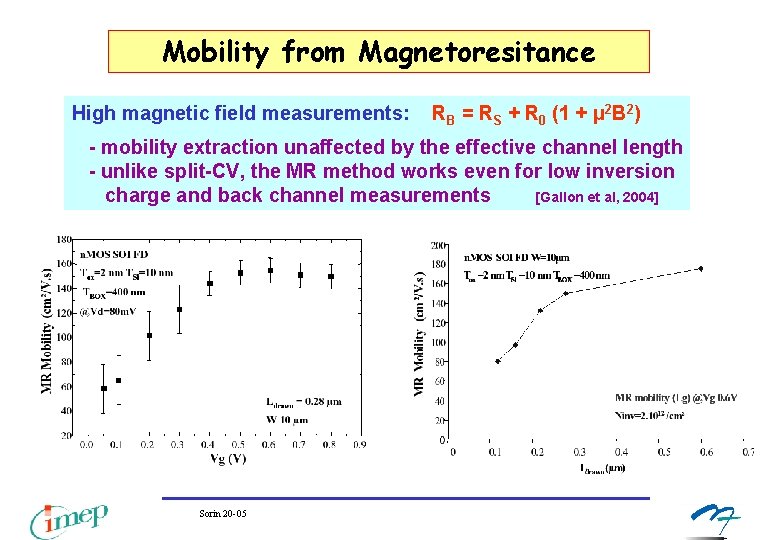
Mobility from Magnetoresitance High magnetic field measurements: RB = RS + R 0 (1 + μ 2 B 2) - mobility extraction unaffected by the effective channel length - unlike split-CV, the MR method works even for low inversion charge and back channel measurements [Gallon et al, 2004] Sorin 20 -05
Superior Radiation Hardness of DG-MOSFETs Lower VT shift in DG mode due to volume inversion [B. Jun et al, 2004] Experiment Sorin 20 -05 Simulations
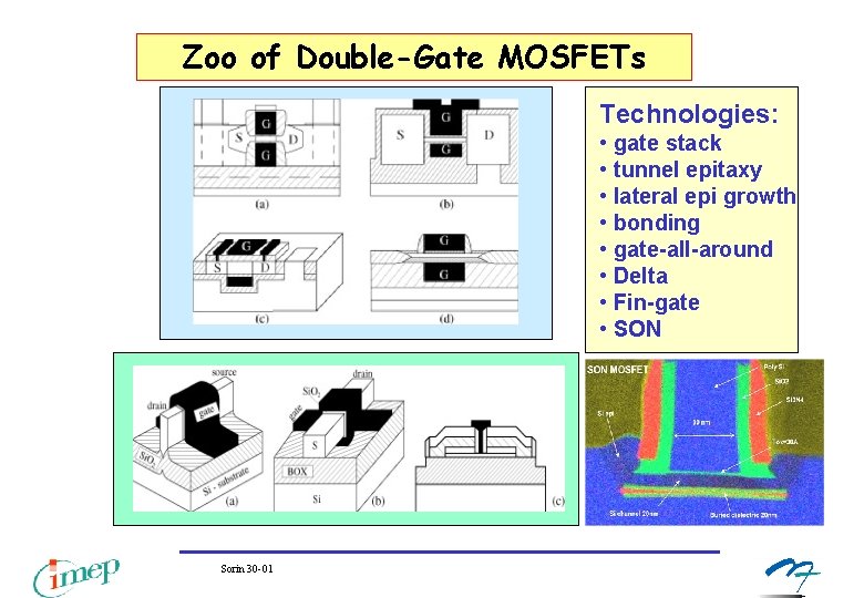
Zoo of Double-Gate MOSFETs Technologies: • gate stack • tunnel epitaxy • lateral epi growth • bonding • gate-all-around • Delta • Fin-gate • SON Sorin 30 -01
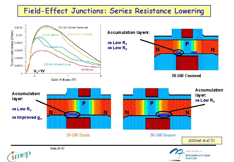
Field-Effect Junctions: Series Resistance Lowering Accumulation layers: Low RS Low RD N VD=1 V Improved gm N 50 -100 Centered Accumulation layer: Low RS P P N 50 -100 Drain Accumulation layer: Low RD N N 50 -100 Source Allibert et al’ 01 Sorin 20 -05
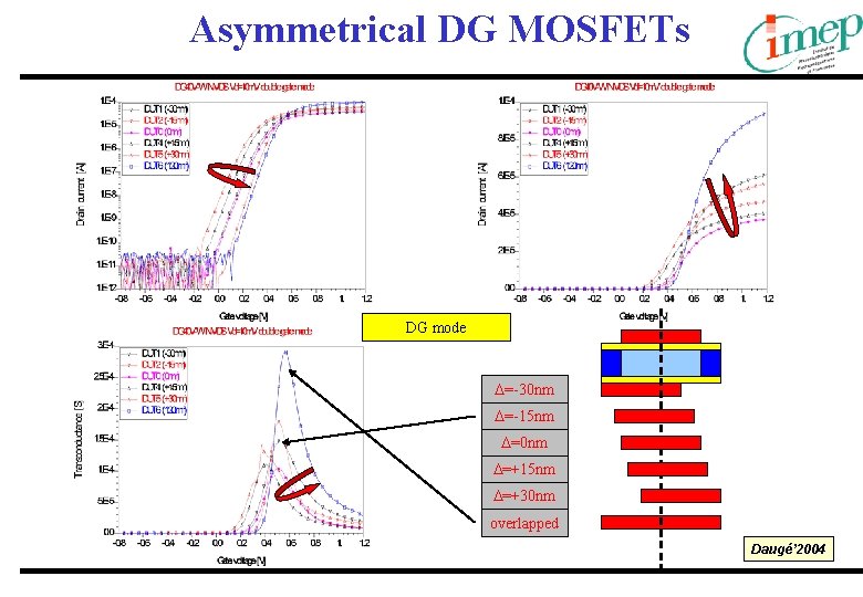
Asymmetrical DG MOSFETs DG mode =-30 nm =-15 nm =0 nm =+15 nm =+30 nm overlapped Daugé’ 2004
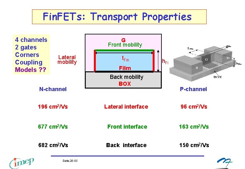
Fin. FETs: Transport Properties 4 channels 2 gates Corners Coupling Models ? ? G Front mobility Lateral mobility N-channel t. Fin Film Back mobility BOX h. Fin P-channel 196 cm 2/Vs Lateral interface 96 cm 2/Vs 677 cm 2/Vs Front interface 163 cm 2/Vs 682 cm 2/Vs Back interface Sorin 20 -05 150 cm 2/Vs
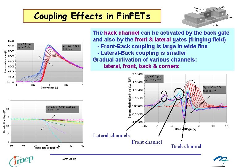
Coupling Effects in Fin. FETs The back channel can be activated by the back gate and also by the front & lateral gates (fringing field) - Front-Back coupling is large in wide fins - Lateral-Back coupling is smaller Gradual activation of various channels: lateral, front, back & corners Lateral channels Front channel Sorin 20 -05 Back channel
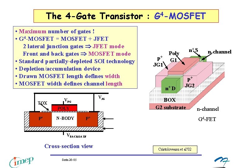
The 4 -Gate Transistor : G 4 -MOSFET • Maximum number of gates ! • G 4 -MOSFET = MOSFET + JFET 2 lateral junction gates JFET mode Front and back gates MOSFET mode • Standard partially-depleted SOI technology • Depletion/accumulation device • Drawn MOSFET length defines width • MOSFET width defines channel length TOX VJG VPG POLY P+ N -BODY n+ S Poly G 1 JG 1 n+ D p+ JG 2 BOX G 2 substrate VBACKGATE Sorin 20 -05 n-channel G 4 -FET P+ Cross-section view n-channel p+ Cristoloveanu et al’ 02
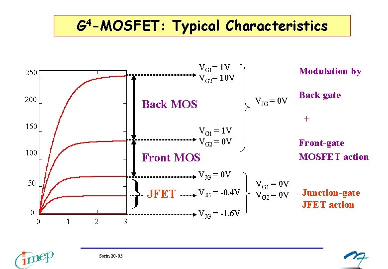
G 4 -MOSFET: Typical Characteristics VG 1= 1 V VG 2= 10 V 250 200 Back MOS VJG = 0 V Back gate + 150 VG 1 = 1 V VG 2 = 0 V 100 Front-gate MOSFET action Front MOS } 50 0 0 Modulation by 1 2 3 Sorin 20 -05 VJG = 0 V JFET VJG = -0. 4 V VJG = -1. 6 V VG 1 = 0 V VG 2 = 0 V Junction-gate JFET action
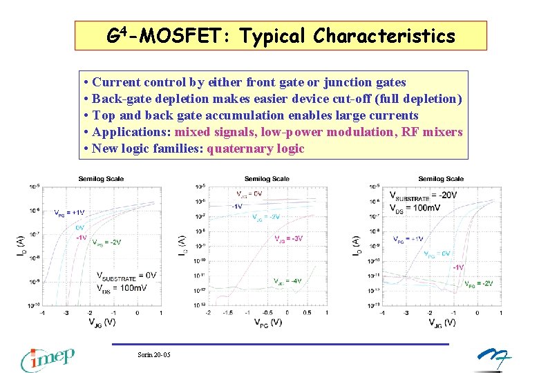
G 4 -MOSFET: Typical Characteristics • Current control by either front gate or junction gates • Back-gate depletion makes easier device cut-off (full depletion) • Top and back gate accumulation enables large currents • Applications: mixed signals, low-power modulation, RF mixers • New logic families: quaternary logic Sorin 20 -05
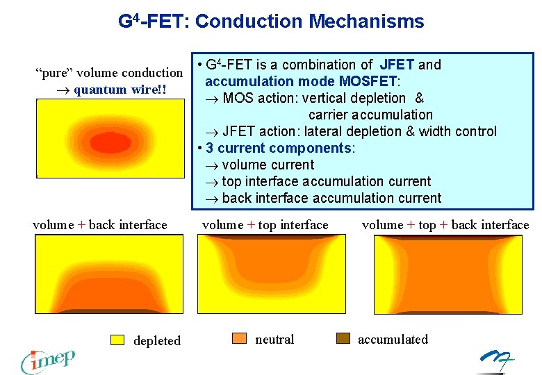
G 4 -FET: Conduction Mechanisms • G 4 -FET is a combination of JFET and “pure” volume conduction accumulation mode MOSFET: quantum wire!! MOS action: vertical depletion & carrier accumulation JFET action: lateral depletion & width control • 3 current components: volume current top interface accumulation current back interface accumulation current volume + back interface depleted volume + top interface neutral volume + top + back interface accumulated
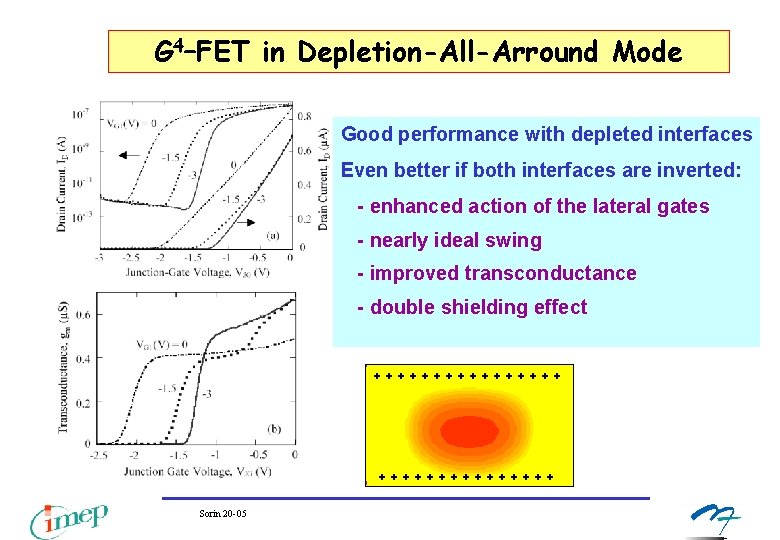
G 4–FET in Depletion-All-Arround Mode Good performance with depleted interfaces Even better if both interfaces are inverted: - enhanced action of the lateral gates - nearly ideal swing - improved transconductance - double shielding effect ++++++++ Sorin 20 -05
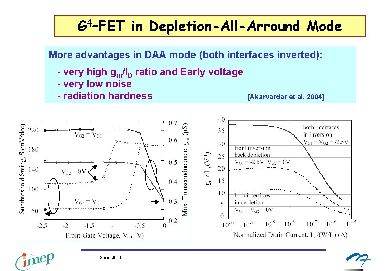
G 4–FET in Depletion-All-Arround Mode More advantages in DAA mode (both interfaces inverted): - very high gm/ID ratio and Early voltage - very low noise - radiation hardness [Akarvardar et al, 2004] Sorin 20 -05
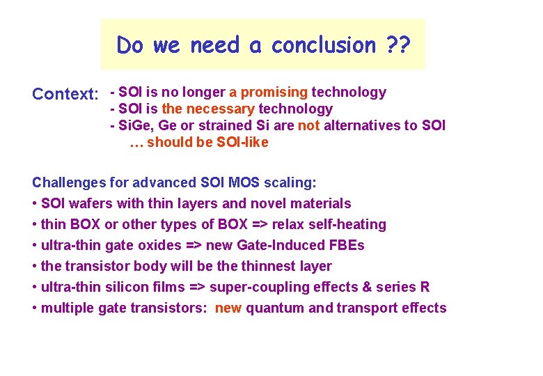
Do we need a conclusion ? ? Context: - SOI is no longer a promising technology - SOI is the necessary technology - Si. Ge, Ge or strained Si are not alternatives to SOI … should be SOI-like Challenges for advanced SOI MOS scaling: • SOI wafers with thin layers and novel materials • thin BOX or other types of BOX => relax self-heating • ultra-thin gate oxides => new Gate-Induced FBEs => • the transistor body will be thinnest layer • ultra-thin silicon films => super-coupling effects & series R • multiple gate transistors: new quantum and transport effects
Questions & More Questions Video Tutorial SOI Technologies: Materials, Devices, Characterization, and Ultimate Architectures http: //isde. vanderbilt. edu/download. php Sorin 20 -05
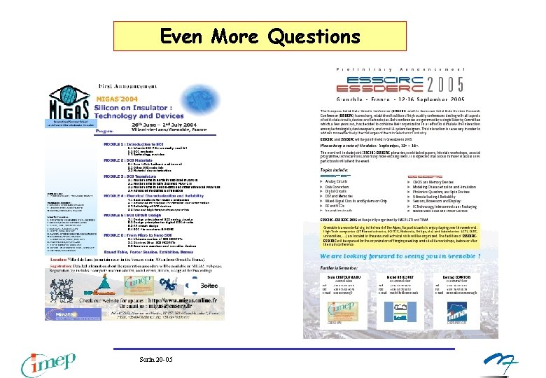
Even More Questions Sorin 20 -05
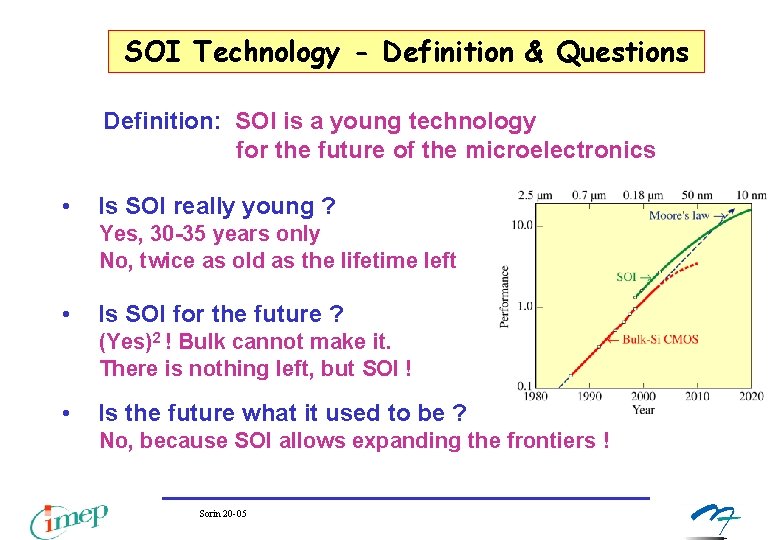
SOI Technology - Definition & Questions Definition: SOI is a young technology for the future of the microelectronics • Is SOI really young ? Yes, 30 -35 years only No, twice as old as the lifetime left • Is SOI for the future ? (Yes)2 ! Bulk cannot make it. There is nothing left, but SOI ! • Is the future what it used to be ? No, because SOI allows expanding the frontiers ! Sorin 20 -05
Scanning analysis - Simulations The time dependence is fully reproduced by simulation: Competition between body charging by gate-to-body tunneling current and capacitive coupling (overshoot : high VB which drops via recombination). For slow scan : - the body charging by the gate current occurs earlier - the 2 nd peak shifts to lower VG Sorin 20 -05
Distribution of Fringing Fields in SOI MOSFETs Analytical model based on conformal mapping Ernst et al’ 99 Sorin 20 -05
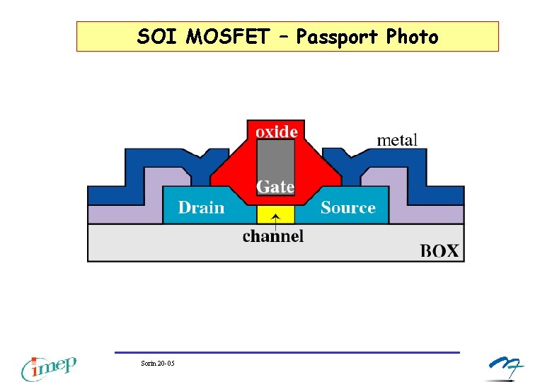
SOI MOSFET – Passport Photo Sorin 20 -05
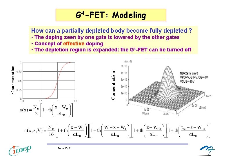
G 4 -FET: Modeling How can a partially depleted body become fully depleted ? Concentration • The doping seen by one gate is lowered by the other gates • Concept of effective doping • The depletion region is expanded: the G 4 -FET can be turned off Sorin 20 -05
Effective Doping: PD-FD Transition Revisited Classical transition : WG = tsi The transition actually depends on channel length • The doping seen by the gate is lowered by source and drain • Doping-Length transformation ; see also Doping-Voltage transformation [Magy’ 88] 5 1017 Neff 4 1017 3 1017 2 1017 1 1017 S D 0 -1 1017 Sorin 20 -05
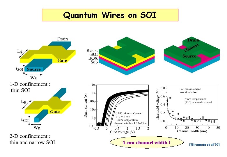
Quantum Wires on SOI 1 -nm channel width !
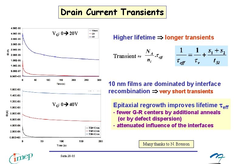
Drain Current Transients VG: 0 20 V Higher lifetime longer transients Transient 10 nm films are dominated by interface recombination very short transients VG: 0 40 V Epitaxial regrowth improves lifetime eff - fewer G-R centers by additional anneals (or by defect dispersion) - attenuated influence of the interfaces Many thanks to N. Bresson Sorin 20 -05
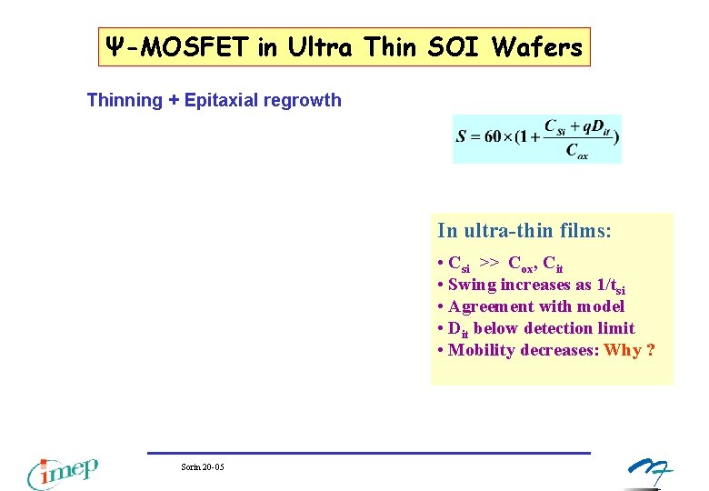
Ψ-MOSFET in Ultra Thin SOI Wafers Thinning + Epitaxial regrowth In ultra-thin films: • Csi >> Cox, Cit • Swing increases as 1/tsi • Agreement with model • Dit below detection limit • Mobility decreases: Why ? Sorin 20 -05
Self-Heating in SOI MOSFETs Sorin 20 -05
Self-Heating in SOI MOSFETs Sorin 20 -05