
OUTLINE 1 2 3 4 5 Introduction SOI

- Slides: 28
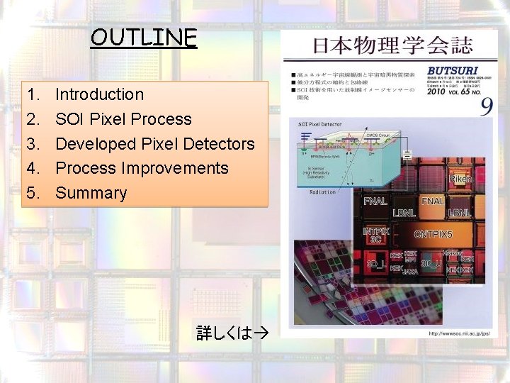
OUTLINE 1. 2. 3. 4. 5. Introduction SOI Pixel Process Developed Pixel Detectors Process Improvements Summary 詳しくは
Silicon-On-Insulator (SOI) Wafer Smart. Cut (1991) Michel. Bruel Leti(仏)) Layer Transfer 3
Metal contact & p+ implant 1 st Al Handle Wafer Copyright 2007 Oki Electric Industry Co. , Ltd 6
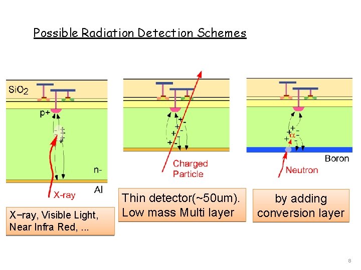
Possible Radiation Detection Schemes X−ray, Visible Light, Near Infra Red, . . . Thin detector(~50 um). Low mass Multi layer by adding conversion layer 8
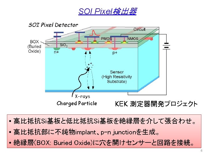
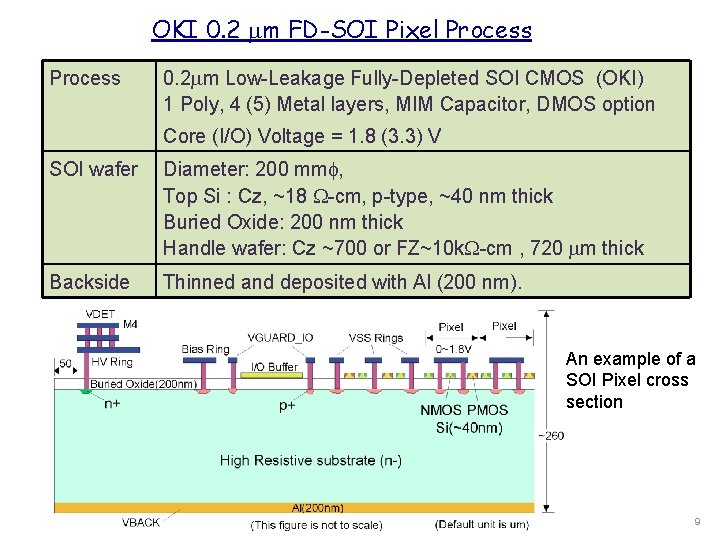
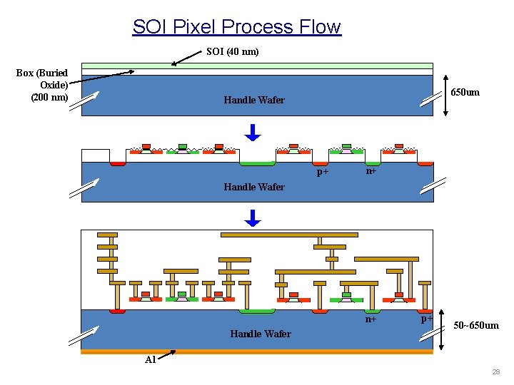
OKI 0. 2 m FD-SOI Pixel Process 0. 2 m Low-Leakage Fully-Depleted SOI CMOS (OKI) 1 Poly, 4 (5) Metal layers, MIM Capacitor, DMOS option Core (I/O) Voltage = 1. 8 (3. 3) V SOI wafer Diameter: 200 mm , Top Si : Cz, ~18 -cm, p-type, ~40 nm thick Buried Oxide: 200 nm thick Handle wafer: Cz ~700 or FZ~10 k -cm , 720 m thick Backside Thinned and deposited with Al (200 nm). An example of a SOI Pixel cross section 9
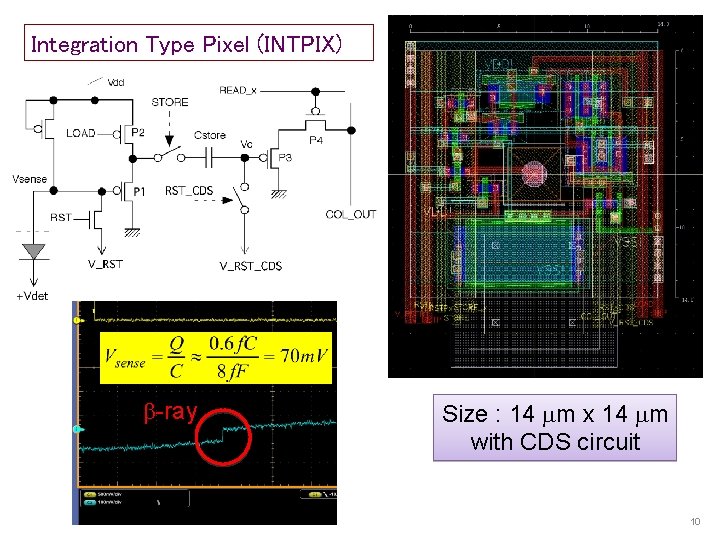
Integration Type Pixel (INTPIX) b-ray Size : 14 m x 14 m with CDS circuit 10
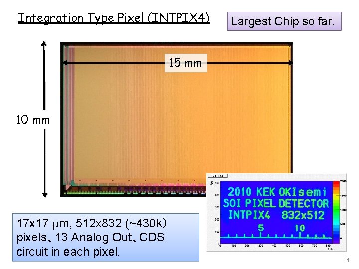
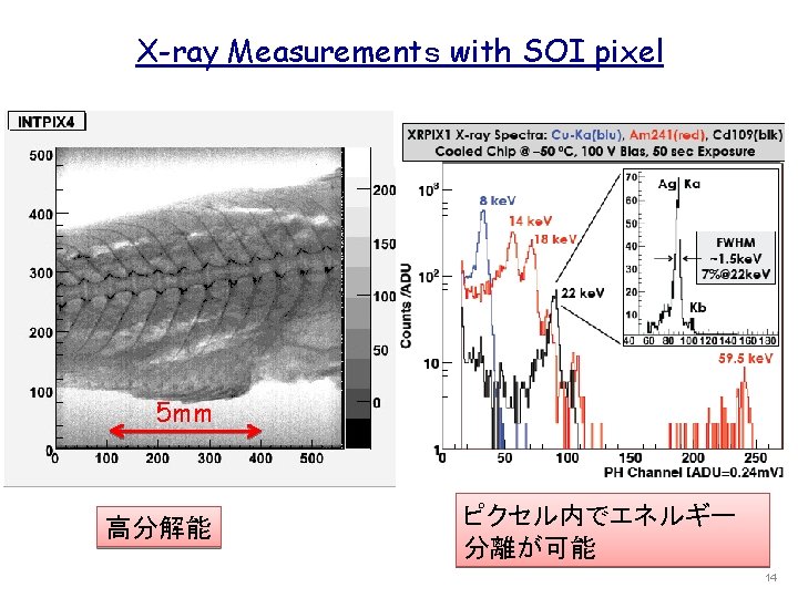
Integration Type Pixel (INTPIX 4) Largest Chip so far. 15 mm 10 mm 17 x 17 m, 512 x 832 (~430 k) pixels、13 Analog Out、CDS circuit in each pixel. 11
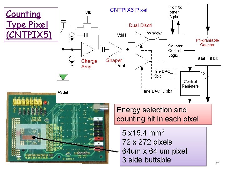
Counting Type Pixel (CNTPIX 5) Energy selection and counting hit in each pixel 5 x 15. 4 mm 2 72 x 272 pixels 64 um x 64 um pixel 3 side buttable 12
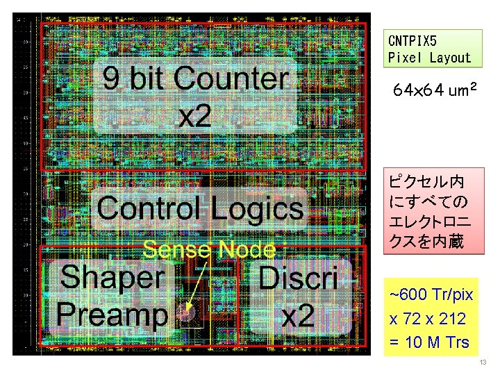
CNTPIX 5 Pixel Layout 64 x 64 um 2 ピクセル内 にすべての エレクトロニ クスを内蔵 ~600 Tr/pix x 72 x 212 = 10 M Trs 13
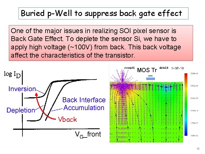
Buried p-Well to suppress back gate effect One of the major issues in realizing SOI pixel sensor is Back Gate Effect. To deplete the sensor Si, we have to apply high voltage (~100 V) from back. This back voltage affect the characteristics of the transistor. MOS Tr Vback 15
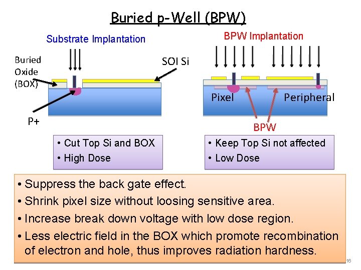
Buried p-Well (BPW) BPW Implantation Substrate Implantation SOI Si Buried Oxide (BOX) Pixel P+ Peripheral BPW • Cut Top Si and BOX • High Dose • Keep Top Si not affected • Low Dose • Suppress the back gate effect. • Shrink pixel size without loosing sensitive area. • Increase break down voltage with low dose region. • Less electric field in the BOX which promote recombination of electron and hole, thus improves radiation hardness. 16
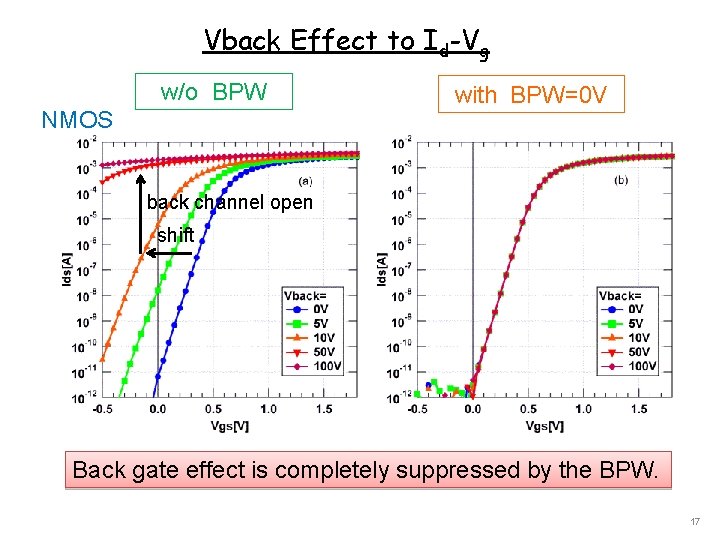
Vback Effect to Id-Vg w/o BPW NMOS with BPW=0 V back channel open shift Back gate effect is completely suppressed by the BPW. 17
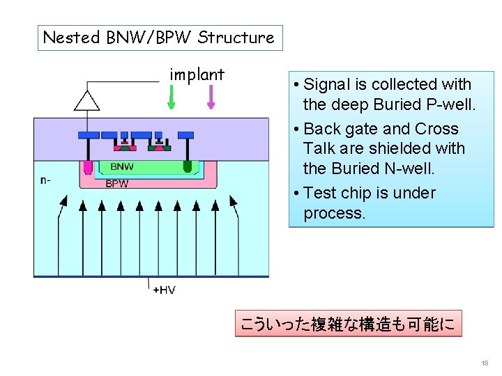
Nested BNW/BPW Structure implant • Signal is collected with the deep Buried P-well. • Back gate and Cross Talk are shielded with the Buried N-well. • Test chip is under process. こういった複雑な構造も可能に 18
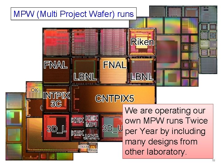
MPW (Multi Project Wafer) runs We are operating our own MPW runs Twice per Year by including many designs from other laboratory. 19
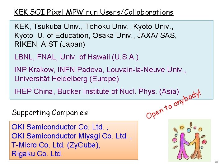
KEK SOI Pixel MPW run Users/Collaborations KEK, Tsukuba Univ. , Tohoku Univ. , Kyoto U. of Education, Osaka Univ. , JAXA/ISAS, RIKEN, AIST (Japan) LBNL, FNAL, Univ. of Hawaii (U. S. A. ) INP Krakow, INFN Padova, Louvain-la-Neuve Univ. , Universität Heidelberg (Europe) IHEP China, Budker Institute of Nucl. Phys. (Asia) Supporting Companies en p O t ny a o ! y d bo OKI Semiconductor Co. Ltd. , OKI Semiconductor Miyagi Co. Ltd. , T-Micro Co. Ltd. (Zy. Cube), Rigaku Co. Ltd. 20
Supplement 22
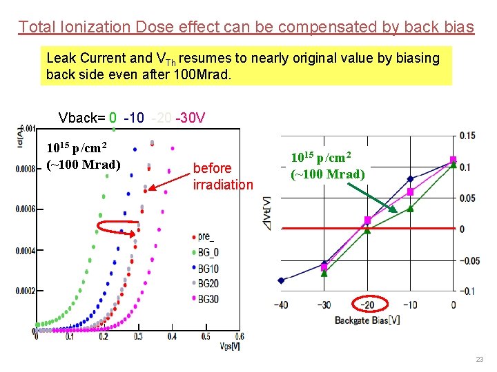
Total Ionization Dose effect can be compensated by back bias Leak Current and VTh resumes to nearly original value by biasing back side even after 100 Mrad. Vback= 0 -10 -20 -30 V 1015 p/cm 2 (~100 Mrad) before irradiation 1015 p/cm 2 (~100 Mrad) 23
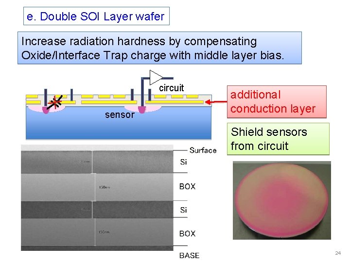
e. Double SOI Layer wafer Increase radiation hardness by compensating Oxide/Interface Trap charge with middle layer bias. circuit sensor additional conduction layer Shield sensors from circuit 24
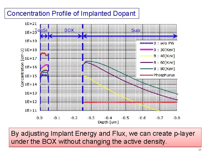
Concentration Profile of Implanted Dopant By adjusting Implant Energy and Flux, we can create p-layer under the BOX without changing the active density. 25
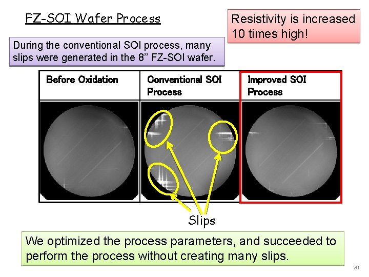
FZ-SOI Wafer Process During the conventional SOI process, many slips were generated in the 8’’ FZ-SOI wafer. Before Oxidation Conventional SOI Process Resistivity is increased 10 times high! Improved SOI Process Slips We optimized the process parameters, and succeeded to perform the process without creating many slips. 26
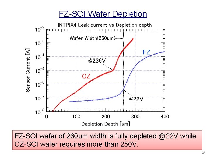
FZ-SOI Wafer Depletion FZ-SOI wafer of 260 um width is fully depleted @22 V while CZ-SOI wafer requires more than 250 V. 27
SOI Pixel Process Flow SOI (40 nm) Box (Buried Oxide) (200 nm) 650 um Handle Wafer p+ n+ Handle Wafer p+ 50~650 um Al 28