Silicon on Insulator Advanced Electronic Devices Karthik Swaminathan
- Slides: 25

Silicon on Insulator Advanced Electronic Devices Karthik Swaminathan

Reasons for SOI • Replacement for SOS • Need to extend Moore’s Law • Commercial Availability of SOI wafers

Advantages of SOI • Reduced Source and Drain to Substrate Capacitance. • Absence of Latchup. • Lower Passive current. • Denser Layout Low cost.

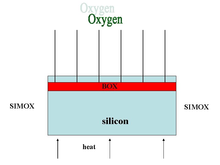
SOI Wafer Fabrication • Bond and Etch Back • SIMOX (Separation by IMplantation Of o. Xygen) • SIMON(Separation by IMplantation Of Nitrogen)

BOX SIMOX silicon heat

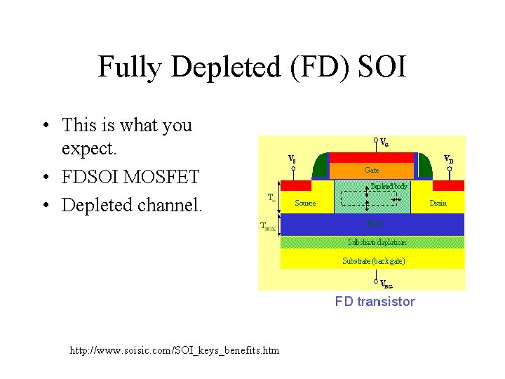
Fully Depleted (FD) SOI • This is what you expect. • FDSOI MOSFET • Depleted channel. http: //www. soisic. com/SOI_keys_benefits. htm

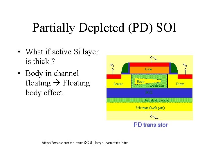
Partially Depleted (PD) SOI • What if active Si layer is thick ? • Body in channel floating Floating body effect. http: //www. soisic. com/SOI_keys_benefits. htm

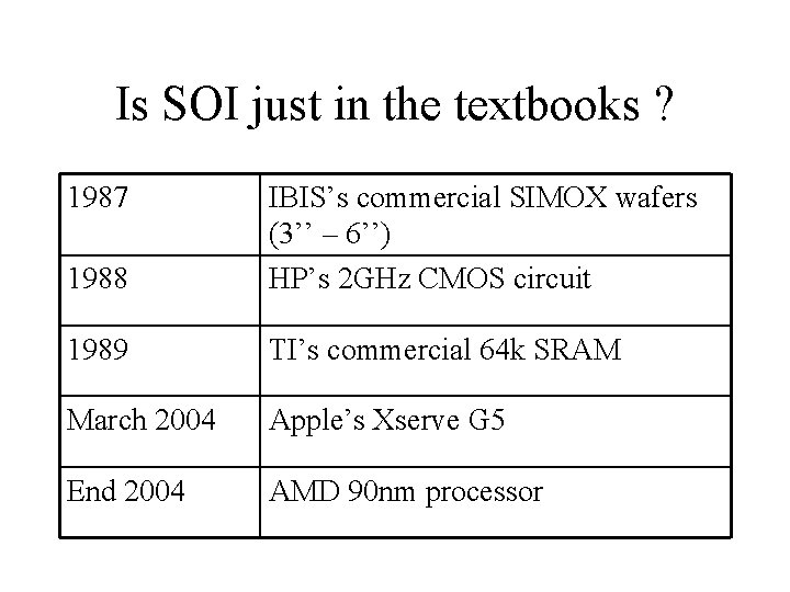
Is SOI just in the textbooks ? 1987 1988 IBIS’s commercial SIMOX wafers (3’’ – 6’’) HP’s 2 GHz CMOS circuit 1989 TI’s commercial 64 k SRAM March 2004 Apple’s Xserve G 5 End 2004 AMD 90 nm processor

Novel SOI Devices • Dual gate SOI. • SOI Single electron transistors.

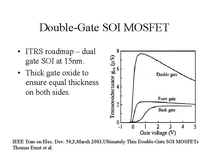
Double-Gate SOI MOSFET • ITRS roadmap – dual gate SOI at 15 nm. • Thick gate oxide to ensure equal thickness on both sides. IEEE Tran on Elec. Dev. 50, 3, March 2003, Ultimately Thin Double-Gate SOI MOSFETs Thomas Ernst et al.

Issues – Negative resist for EBL • PMMA resist is a good positive resist for EBL. • Do we have a good negative EBL resist high resolution. • NO alternate techniques.

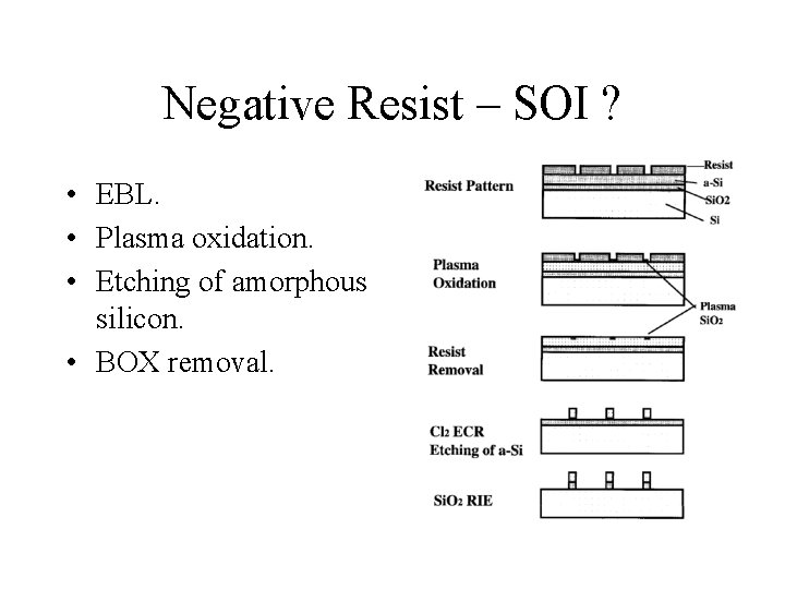
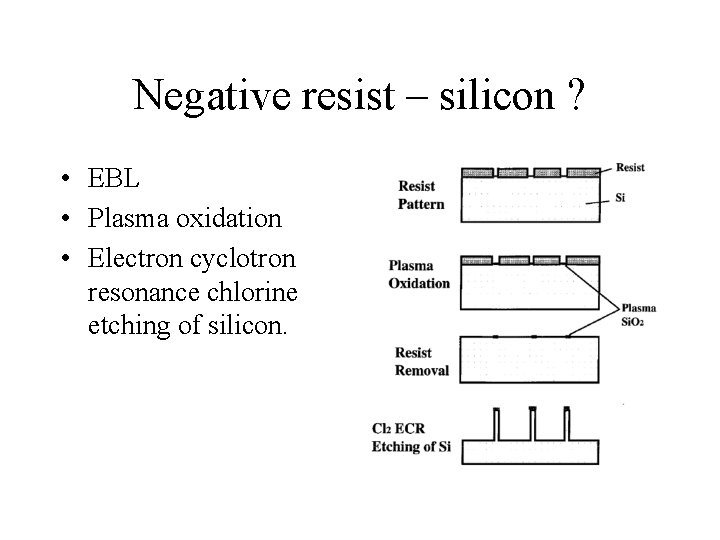
Negative Resist – SOI ? • EBL. • Plasma oxidation. • Etching of amorphous silicon. • BOX removal.

Negative resist – silicon ? • EBL • Plasma oxidation • Electron cyclotron resonance chlorine etching of silicon.

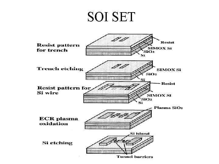
SOI SET

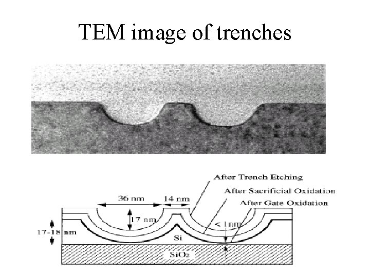
TEM image of trenches

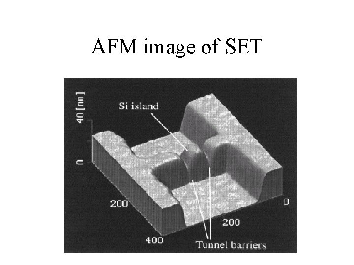
AFM image of SET

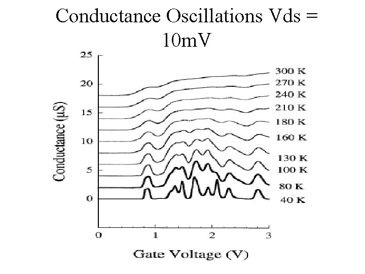
Conductance Oscillations Vds = 10 m. V

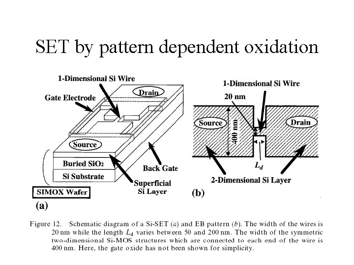
SET by pattern dependent oxidation

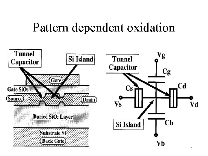
Pattern dependent oxidation

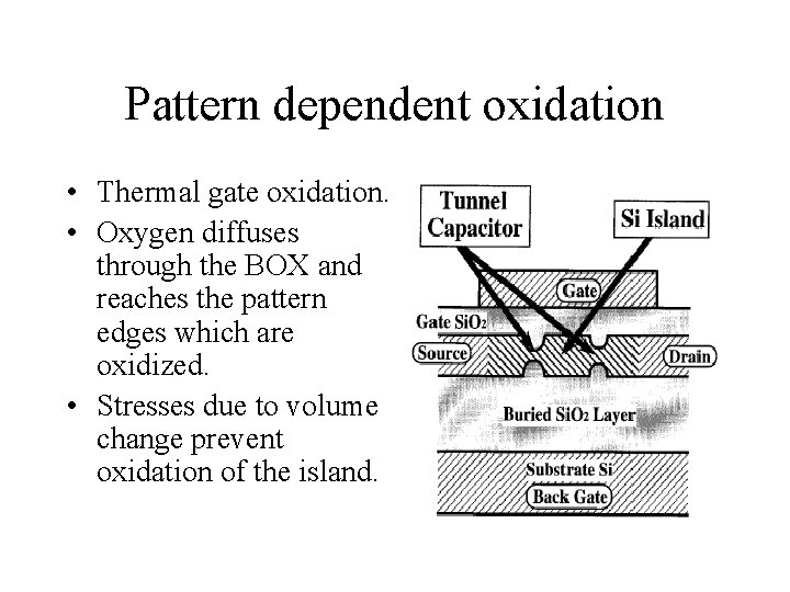
Pattern dependent oxidation • Thermal gate oxidation. • Oxygen diffuses through the BOX and reaches the pattern edges which are oxidized. • Stresses due to volume change prevent oxidation of the island.

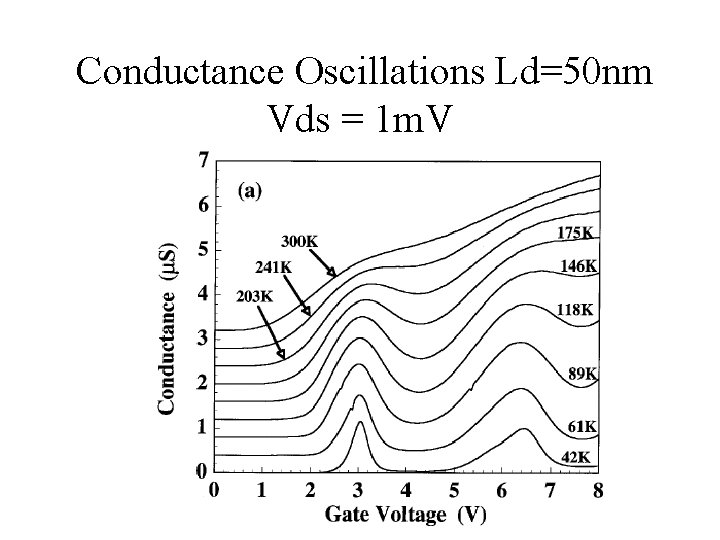
Conductance Oscillations Ld=50 nm Vds = 1 m. V

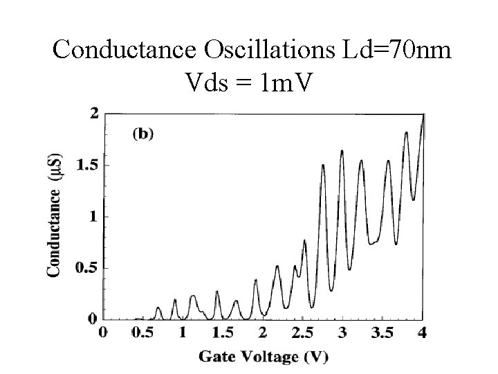
Conductance Oscillations Ld=70 nm Vds = 1 m. V

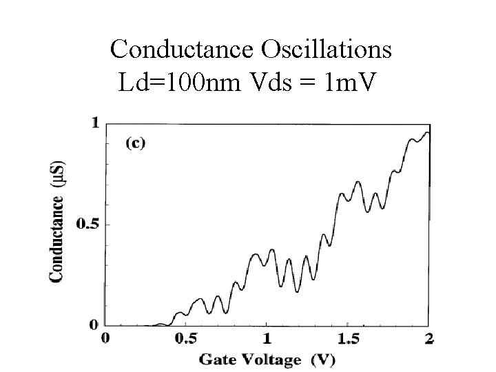
Conductance Oscillations Ld=100 nm Vds = 1 m. V

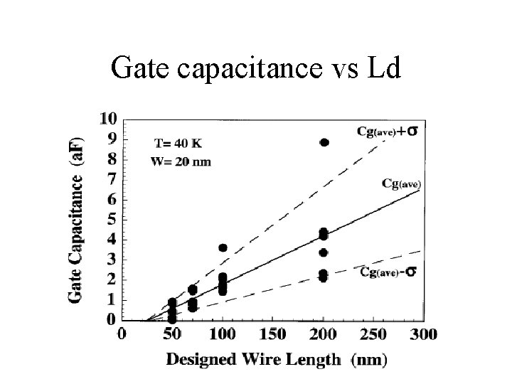
Gate capacitance vs Ld

Summary • Future devices will involve SOI. • SOI provides certain benefits over bulk CMOS for smaller gate lengths. • SOI SETs may become a promising technology in the future.