
SOIEnabled 3 D Integrated Circuit Technology TIPP 2011
SOI-Enabled 3 D Integrated Circuit Technology TIPP 2011 14 June 2011 C. K. Chen, B Wheeler, D. R. W. Yost, J. M. Knecht, and C. L. Keast MIT Lincoln Laboratory *This work was sponsored by the Defense Advanced Research Projects Agency under Air Force contract #FA 8721 -05 -C 0002. Opinions, interpretations, conclusions, and recommendations are those of the authors and are not necessarily endorsed by the United States Government. TIPP 2011 p 1 14 June 2011 ckc MIT Lincoln Laboratory

Why 3 D? Exploiting Different Process Technologies High Performance m-Processors Density, Speed, & Power 3 DIC Cross Section Mixed Material Integration Compound Semiconductors TIPP 2011 p 2 14 June 2011 ckc Advanced Focal Plane Imagers 100% Fill Factor MIT Lincoln Laboratory
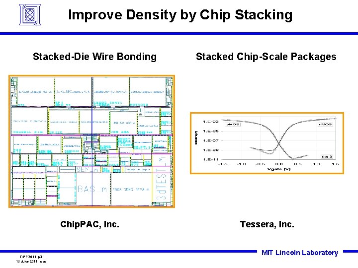
Improve Density by Chip Stacking Stacked-Die Wire Bonding Stacked Chip-Scale Packages 1 mm Chip. PAC, Inc. TIPP 2011 p 3 14 June 2011 ckc Tessera, Inc. MIT Lincoln Laboratory
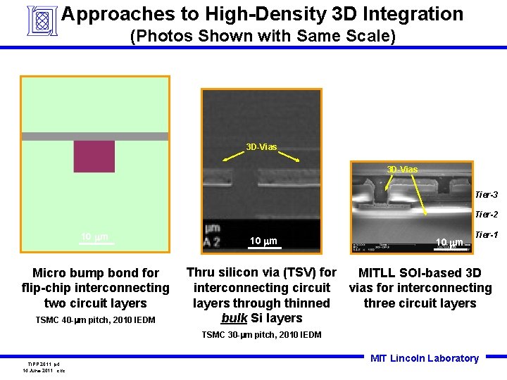
Approaches to High-Density 3 D Integration (Photos Shown with Same Scale) 3 D-Vias Tier-3 Tier-2 10 mm Micro bump bond for flip-chip interconnecting two circuit layers TSMC 40 -mm pitch, 2010 IEDM 10 mm Tier-1 Thru silicon via (TSV) for MITLL SOI-based 3 D interconnecting circuit vias for interconnecting layers through thinned three circuit layers bulk Si layers TSMC 30 -mm pitch, 2010 IEDM TIPP 2011 p 4 14 June 2011 ckc MIT Lincoln Laboratory
Outline • • TIPP 2011 p 5 14 June 2011 ckc Motivation Lincoln’s 3 D Integrated Circuit Process 3 D Circuit Demonstrations Summary MIT Lincoln Laboratory
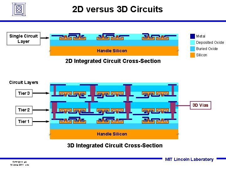
2 D versus 3 D Circuits Single Circuit Layer Metal Deposited Oxide Handle Silicon Buried Oxide Silicon 2 D Integrated Circuit Cross-Section Circuit Layers Tier 3 3 D Vias Tier 2 Tier 1 Handle Silicon 3 D Integrated Circuit Cross-Section TIPP 2011 p 6 14 June 2011 ckc MIT Lincoln Laboratory
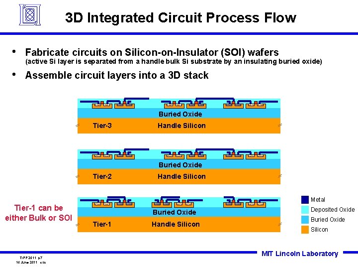
3 D Integrated Circuit Process Flow • Fabricate circuits on Silicon-on-Insulator (SOI) wafers • Assemble circuit layers into a 3 D stack (active Si layer is separated from a handle bulk Si substrate by an insulating buried oxide) Buried Oxide Tier-3 Handle Silicon Buried Oxide Tier-2 Handle Silicon Metal Tier-1 can be either Bulk or SOI TIPP 2011 p 7 14 June 2011 ckc Buried Oxide Tier-1 Handle Silicon Deposited Oxide Buried Oxide Silicon MIT Lincoln Laboratory
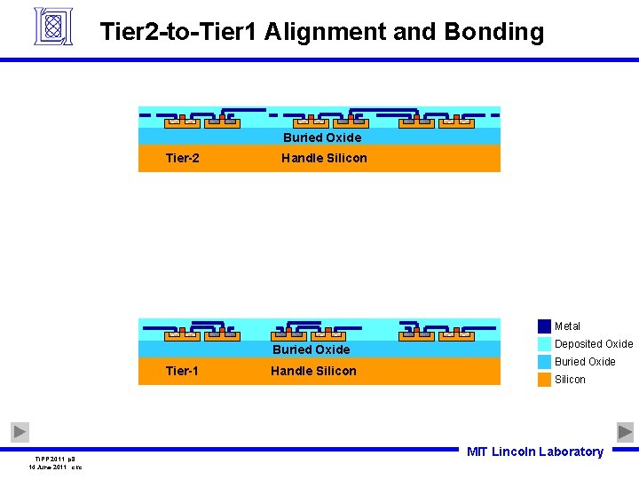
Tier 2 -to-Tier 1 Alignment and Bonding Buried Oxide Tier-2 Handle Silicon Metal Buried Oxide Tier-1 TIPP 2011 p 8 14 June 2011 ckc Handle Silicon Deposited Oxide Buried Oxide Silicon MIT Lincoln Laboratory
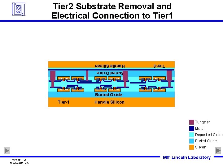
Tier 2 Substrate Removal and Electrical Connection to Tier 1 Tier-2 Handle Silicon Buried Oxide Tier-1 Handle Silicon Tungsten Metal Deposited Oxide Buried Oxide Silicon TIPP 2011 p 9 14 June 2011 ckc MIT Lincoln Laboratory
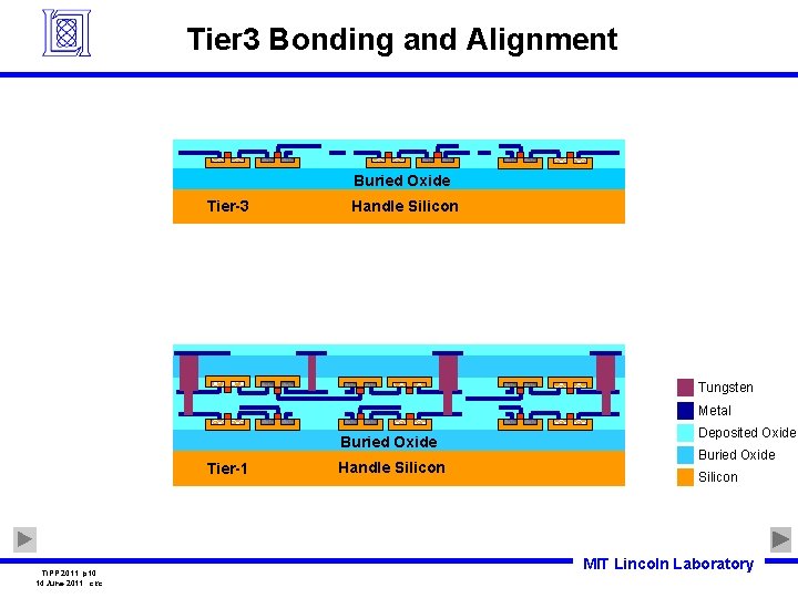
Tier 3 Bonding and Alignment Buried Oxide Tier-3 Handle Silicon Tungsten Metal Buried Oxide Tier-1 TIPP 2011 p 10 14 June 2011 ckc Handle Silicon Deposited Oxide Buried Oxide Silicon MIT Lincoln Laboratory
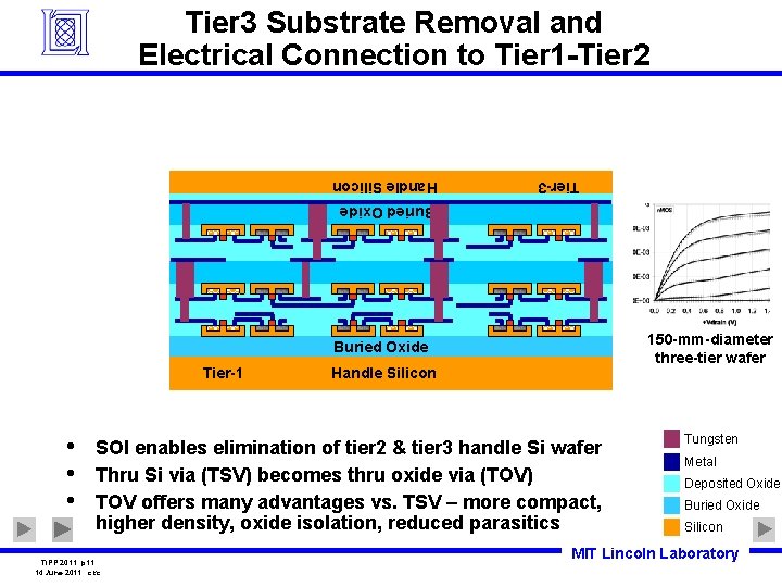
Tier 3 Substrate Removal and Electrical Connection to Tier 1 -Tier 2 Tier-3 Handle Silicon Buried Oxide 150 -mm-diameter three-tier wafer Buried Oxide Tier-1 • • • Handle Silicon SOI enables elimination of tier 2 & tier 3 handle Si wafer Thru Si via (TSV) becomes thru oxide via (TOV) TOV offers many advantages vs. TSV – more compact, higher density, oxide isolation, reduced parasitics TIPP 2011 p 11 14 June 2011 ckc Tungsten Metal Deposited Oxide Buried Oxide Silicon MIT Lincoln Laboratory
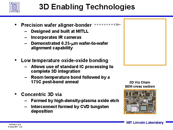
3 D Enabling Technologies • Precision wafer aligner-bonder – Designed and built at MITLL – Incorporates IR cameras – Demonstrated 0. 25 -mm wafer-to-wafer alignment capability • Low temperature oxide-oxide bonding – Allows use of standard IC processing to complete 3 D integration – Room temperature bond followed by a 175 C post-bond anneal • 3 D Via Chain SEM cross section Concentric 3 D via – Formed by high-density-plasma oxide etch – Interconnect formed by CVD tungsten deposition TIPP 2011 p 12 14 June 2011 ckc MIT Lincoln Laboratory
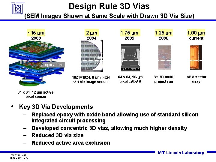
Design Rule 3 D Vias (SEM Images Shown at Same Scale with Drawn 3 D Via Size) ~15 mm 2 mm 1. 75 mm 1. 25 mm 1. 00 mm 2000 2004 2005 2008 current 64 x 64, 50 -mm pixel LADAR 3 rd 3 D multi project run In. P detector array oxide bond epoxy bond 10 um 1024× 1024, 8 -μm pixel visible image sensor 64 x 64, 12 -μm activepixel sensor • Key 3 D Via Developments – Replaced epoxy with oxide bond allowing use of standard silicon integrated circuit processing – Developed concentric 3 D vias, allowing much higher density – Reduced 3 D via size – Reduced active area exclusion TIPP 2011 p 13 14 June 2011 ckc MIT Lincoln Laboratory
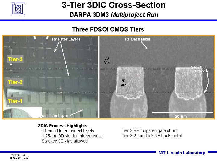
3 -Tier 3 DIC Cross-Section DARPA 3 DM 3 Multiproject Run Three FDSOI CMOS Tiers Transistor Layers Tier-3 RF Back Metal 3 D Via Oxide Bond Interface 3 D Via Tier-2 Tier-1 Transistor Layer 3 DIC Process Highlights 11 metal interconnect levels 1. 25 -mm 3 D via tier interconnect Stacked 3 D vias allowed TIPP 2011 p 14 14 June 2011 ckc 20 mm Tier-3 RF tungsten gate shunt Tier-3 2 -mm-thick RF back metal MIT Lincoln Laboratory
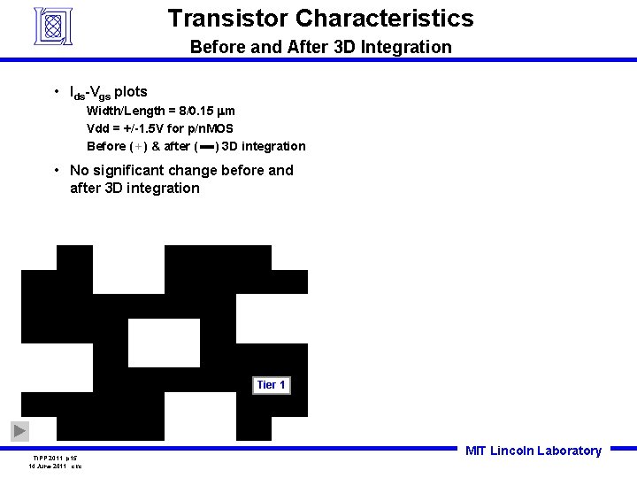
Transistor Characteristics Before and After 3 D Integration • Ids-Vgs plots Width/Length = 8/0. 15 mm Vdd = +/-1. 5 V for p/n. MOS Before ( + ) & after ( ▬ ) 3 D integration • No significant change before and after 3 D integration Tier 2 Tier 1 TIPP 2011 p 15 14 June 2011 ckc Tier 3 MIT Lincoln Laboratory
Outline • • TIPP 2011 p 16 14 June 2011 ckc Motivation Lincoln’s 3 D Integrated Circuit Process 3 D Circuit Demonstrations Summary MIT Lincoln Laboratory
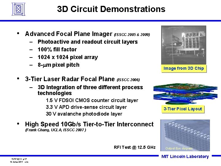
3 D Circuit Demonstrations • Advanced Focal Plane Imager (ISSCC 2005 & 2009) – – • Photoactive and readout circuit layers 100% fill factor 1024 x 1024 pixel array 8 -mm pixel pitch Image from 3 D Chip 3 -Tier Laser Radar Focal Plane (ISSCC 2006) – 3 D Integration of three different process technologies 1. 5 V FDSOI CMOS counter circuit layer 3. 3 V APD drive-sense circuit layer 30 V avalanche photodiode layer • 3 -Tier Pixel Layout High Speed 10 Gb/s Tier-to-Tier Interconnect (Frank Chang, UCLA, ISSCC 2007 ) RFI Test @ 12. 5 GHz TIPP 2011 p 17 14 June 2011 ckc Output Eye diagram MIT Lincoln Laboratory
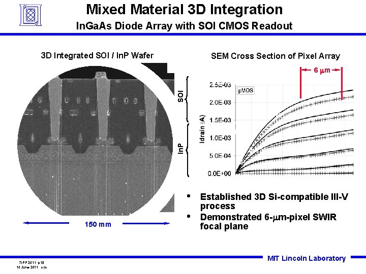
Mixed Material 3 D Integration In. Ga. As Diode Array with SOI CMOS Readout 3 D Integrated SOI / In. P Wafer SEM Cross Section of Pixel Array 6 mm FET 3 D TOV SOI Top metal M 2 M 3 Oxide In. P p In. P In. Ga. As n In. P • 150 mm TIPP 2011 p 18 14 June 2011 ckc • Established 3 D Si-compatible III-V process Demonstrated 6 -mm-pixel SWIR focal plane MIT Lincoln Laboratory
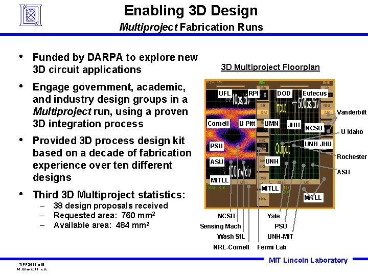
Enabling 3 D Design Multiproject Fabrication Runs • Funded by DARPA to explore new 3 D circuit applications • Engage government, academic, and industry design groups in a Multiproject run, using a proven 3 D integration process • • Provided 3 D process design kit based on a decade of fabrication experience over ten different designs 3 D Multiproject Floorplan UFL RPI 38 design proposals received Requested area: 760 mm 2 Available area: 484 mm 2 Cornell U Pitt UMN JHU NCSU ASU U Idaho UNH JHU PSU Rochester UNH ASU MITLL NCSU Sensing Mach Wash St. L NRL-Cornell TIPP 2011 p 19 14 June 2011 ckc Eutecus Vanderbilt Third 3 D Multiproject statistics: – – – DOD Yale PSU UNH-MIT Fermi Lab MIT Lincoln Laboratory
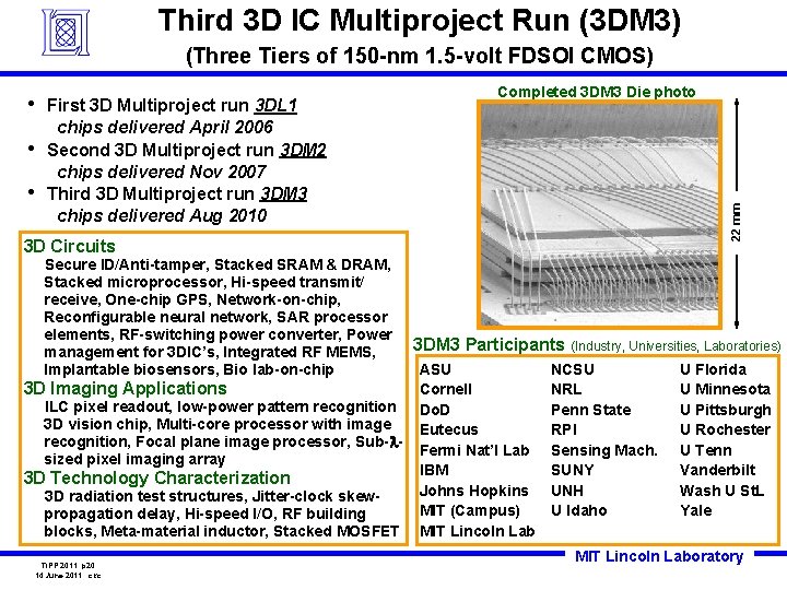
Third 3 D IC Multiproject Run (3 DM 3) (Three Tiers of 150 -nm 1. 5 -volt FDSOI CMOS) • • First 3 D Multiproject run 3 DL 1 chips delivered April 2006 Second 3 D Multiproject run 3 DM 2 chips delivered Nov 2007 Third 3 D Multiproject run 3 DM 3 chips delivered Aug 2010 Completed 3 DM 3 Die photo 22 mm • 3 D Circuits Secure ID/Anti-tamper, Stacked SRAM & DRAM, Stacked microprocessor, Hi-speed transmit/ receive, One-chip GPS, Network-on-chip, Reconfigurable neural network, SAR processor elements, RF-switching power converter, Power management for 3 DIC’s, Integrated RF MEMS, Implantable biosensors, Bio lab-on-chip 3 D Imaging Applications ILC pixel readout, low-power pattern recognition 3 D vision chip, Multi-core processor with image recognition, Focal plane image processor, Sub-lsized pixel imaging array 3 D Technology Characterization 3 D radiation test structures, Jitter-clock skewpropagation delay, Hi-speed I/O, RF building blocks, Meta-material inductor, Stacked MOSFET TIPP 2011 p 20 14 June 2011 ckc 3 DM 3 Participants ASU Cornell Do. D Eutecus Fermi Nat’l Lab IBM Johns Hopkins MIT (Campus) MIT Lincoln Lab (Industry, Universities, Laboratories) NCSU NRL Penn State RPI Sensing Mach. SUNY UNH U Idaho U Florida U Minnesota U Pittsburgh U Rochester U Tenn Vanderbilt Wash U St. L Yale MIT Lincoln Laboratory
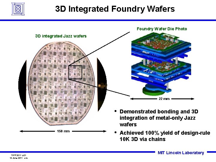
3 D Integrated Foundry Wafers Foundry Wafer Die Photo 3 D integrated Jazz wafers 22 mm 150 mm TIPP 2011 p 21 14 June 2011 ckc • Demonstrated bonding and 3 D integration of metal-only Jazz wafers • Achieved 100% yield of design-rule 10 K 3 D via chains MIT Lincoln Laboratory
Summary • • • SOI-Enabled 3 DIC Process • 3 D Circuit Demonstrations Process characterization TOV (thru oxide via) vs. TSV (thru silicon via) smaller, higher density, reduced parasitics – Advanced Focal Planes (100% fill factor) – 3 D LADAR Chip (mixed technologies) – High Speed 10 Gbps Interconnect – In. P-Si Integration (mixed materials) – 3 D Multiproject Designs • TIPP 2011 p 22 14 June 2011 ckc 3 D Integration of Foundry Wafers MIT Lincoln Laboratory
Supplemental Slides TIPP 2011 p 23 14 June 2011 ckc MIT Lincoln Laboratory
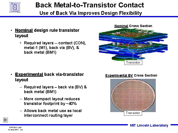
Back Metal-to-Transistor Contact Use of Back Via Improves Design Flexibility • Nominal design rule transistor layout Nominal Cross Section • Required layers -- contact (CON), metal-1 (M 1), back via (BV), & back metal (BM 1) Transistor • Experimental back via-transistor layout Experimental BV Cross Section – Required layers – back via (BV) & back metal (BM 1) – More compact layout reduces transistor footprint by ~40% – Allows back metal use as local interconnect routing layer TIPP 2011 p 24 14 June 2011 ckc Transistor MIT Lincoln Laboratory
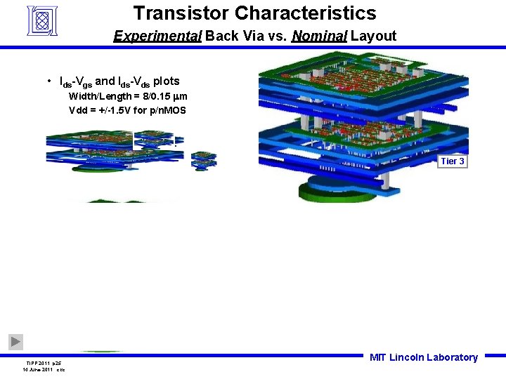
Transistor Characteristics Experimental Back Via vs. Nominal Layout • Ids-Vgs and Ids-Vds plots Width/Length = 8/0. 15 mm Vdd = +/-1. 5 V for p/n. MOS Tier 3 Vg = 0 to -1. 5 V in 0. 25 V steps TIPP 2011 p 25 14 June 2011 ckc Vg = 0 to 1. 5 V in 0. 25 V steps MIT Lincoln Laboratory
- Slides: 25