
MIMOSIS the CMOS Pixel Sensor for the CBM
MIMOSIS, the CMOS Pixel Sensor for the CBM Micro-Vertex Detector Frédéric Morel on behalf of the m. Ic. PHC team of IPHC and IKF team
Outline • MVD • Requirements • MIMOSIS • Global architecture • MIMOSIS 0 • Preliminary results • Conclusion TWEPP 2018 frederic. morel@iphc. cnrs. fr • Introduction 18/09/2018 • CBM 2
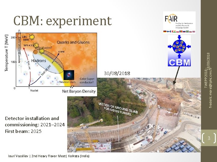
30/08/2018 TWEPP 2018 18/09/2018 frederic. morel@iphc. cnrs. fr CBM: experiment Detector installation and commissioning: 2021– 2024 First beam: 2025 3 Iouri Vassiliev | 2 nd Heavy Flavor Meet| Kolkata (India)
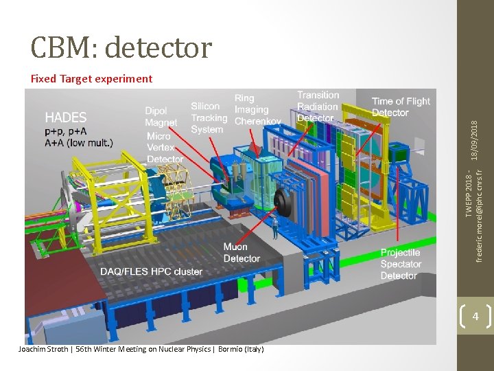
CBM: detector TWEPP 2018 frederic. morel@iphc. cnrs. fr 18/09/2018 Fixed Target experiment 4 Joachim Stroth | 56 th Winter Meeting on Nuclear Physics | Bormio (Italy)
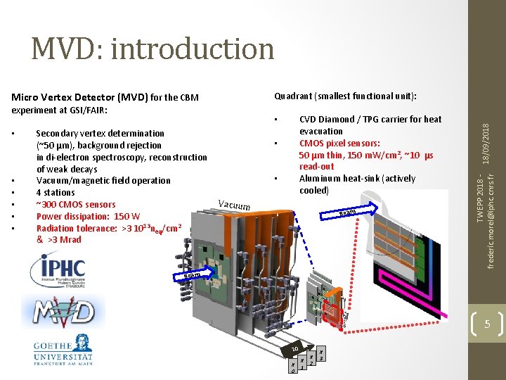
MVD: introduction • • • CVD Diamond / TPG carrier for heat evacuation CMOS pixel sensors: 50 µm thin, 150 m. W/cm², ~10 µs read-out Aluminum heat-sink (actively cooled) • Secondary vertex determination (~50 µm), background rejection in di-electron spectroscopy, reconstruction of weak decays Vacuum/magnetic field operation 4 stations ~300 CMOS sensors Power dissipation: 150 W Radiation tolerance: >3 1013 neq/cm 2 & >3 Mrad • • Vacuum Beam TWEPP 2018 frederic. morel@iphc. cnrs. fr experiment at GSI/FAIR: 18/09/2018 Quadrant (smallest functional unit): Micro Vertex Detector (MVD) for the CBM Beam ea B m 5 20 cm # 0 # 1 # 2 # 3
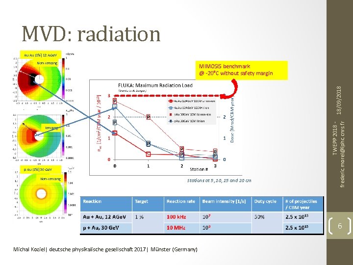
MVD: radiation Au Au (1%) 12 AGe. V Non-ionizing Ionizing p Au (1%) 30 Ge. V Non-ionizing Stations at 5, 10, 15 and 20 cm TWEPP 2018 frederic. morel@iphc. cnrs. fr 18/09/2018 MIMOSIS benchmark @ -20°C without safety margin 6 Michal Koziel| deutsche physikalische gesellschaft 2017| Münster (Germany)
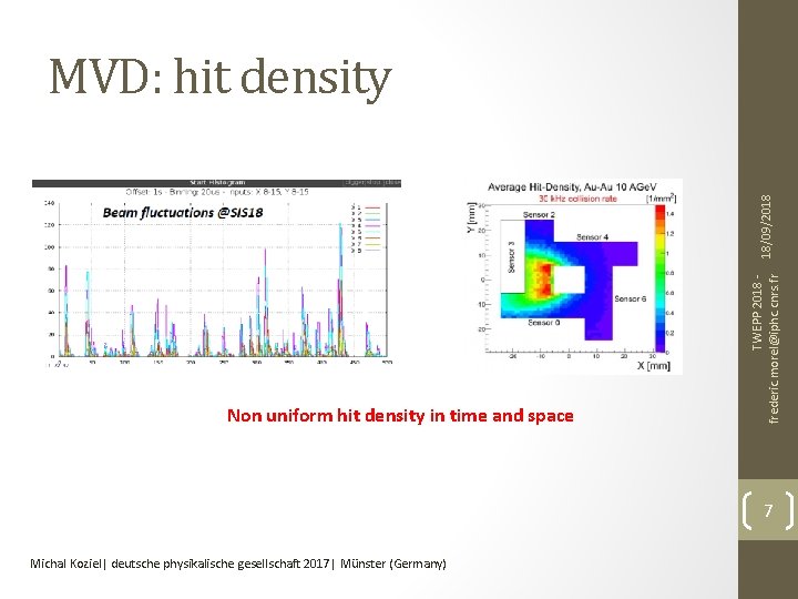
Non uniform hit density in time and space TWEPP 2018 frederic. morel@iphc. cnrs. fr 18/09/2018 MVD: hit density 7 Michal Koziel| deutsche physikalische gesellschaft 2017| Münster (Germany)
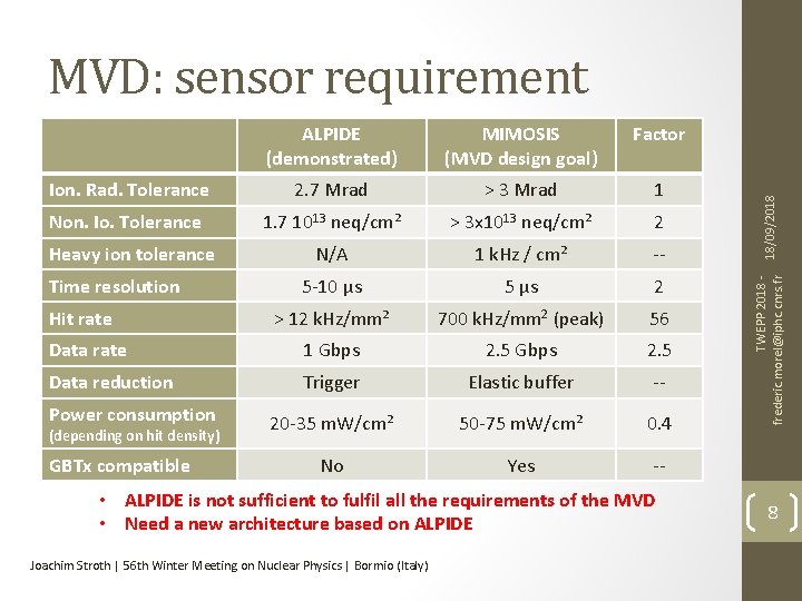
MIMOSIS (MVD design goal) Factor Ion. Rad. Tolerance 2. 7 Mrad > 3 Mrad 1 Non. Io. Tolerance 1. 7 1013 neq/cm² > 3 x 10¹³ neq/cm² 2 N/A 1 k. Hz / cm² -- 5 -10 μs 5 μs 2 > 12 k. Hz/mm² 700 k. Hz/mm 2 (peak) 56 Data rate 1 Gbps 2. 5 Data reduction Trigger Elastic buffer -- 20 -35 m. W/cm² 50 -75 m. W/cm² 0. 4 No Yes -- Heavy ion tolerance Time resolution Hit rate Power consumption (depending on hit density) GBTx compatible • ALPIDE is not sufficient to fulfil all the requirements of the MVD • Need a new architecture based on ALPIDE Joachim Stroth | 56 th Winter Meeting on Nuclear Physics | Bormio (Italy) TWEPP 2018 frederic. morel@iphc. cnrs. fr ALPIDE (demonstrated) 18/09/2018 MVD: sensor requirement 8
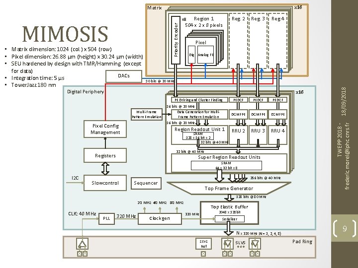
x 16 Matrix Region 1 504 x 2 x 8 pixels x 8 Reg. 3 Reg. 4 PEDCF DGMFPE RRU 2 RRU 3 RRU 4 Pixel Pixel Dig Analog FE 10 bits @ 20 MHz Digital Periphery Multi-Frame Pattern Emulation Pixel Config Management 16 bits @ 20 MHz Data Generation for Multi. Frame Pattern Emulation 16 bits @ 20 MHz Region Readout Unit 1 SRAM 128 x 16 bit x 2 32 bits @ 40 MHz TWEPP 2018 frederic. morel@iphc. cnrs. fr x 16 PE Driving and Cluster Finding 32 bits @ 40 MHz Registers Super Region Readout Units SRAM 64 x 32 bit x 8 I 2 C Slowcontrol 256 bits @ 40 MHz Sequencer 18/09/2018 • Matrix dimension: 1024 (col. ) x 504 (row) • Pixel dimension: 26. 88 µm (height) x 30. 24 µm (width) • SEU hardened by design with TMR/Hamming (except for data) DACs • Integration time: 5 µs • Tower. Jazz 180 nm Priority Encoder MIMOSIS Reg. 2 Top Frame Generator 128 bits @ 80 MHz 20 MHz 40 MHz 80 MHz CLK: 40 MHz PLL 320 MHz Clock gen Top Elastic Buffer 2048 x 128 bit 320 MHz Serializer 9 N x 320 MHz (N = 1, 2, 4, 8) SLVS Ref SLVS Pad Ring
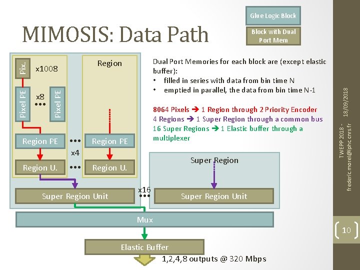
Glue Logic Block Region PE • • • 8064 Pixels 1 Region through 2 Priority Encoder 4 Regions 1 Super Region through a common bus 16 Super Regions 1 Elastic buffer through a multiplexer Region PE x 4 Region U. • • • Super Region Unit x 16 • • • Super Region Unit Mux Elastic Buffer 1, 2, 4, 8 outputs @ 320 Mbps 18/09/2018 • • • TWEPP 2018 frederic. morel@iphc. cnrs. fr x 8 Block with Dual Port Memories for each block are (except elastic buffer): • filled in series with data from bin time N • emptied in parallel, the data from bin time N-1 Region Pixel PE Pix. x 1008 Pixel PE MIMOSIS: Data Path 10
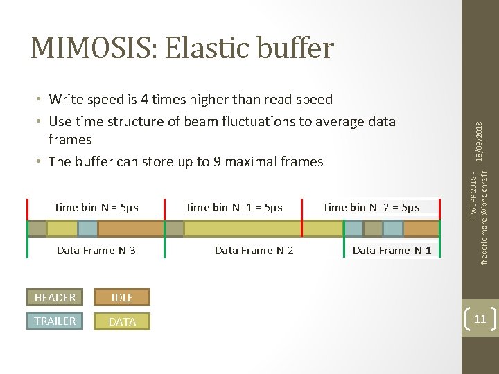
Time bin N = 5µs Data Frame N-3 HEADER IDLE TRAILER DATA Time bin N+1 = 5µs Data Frame N-2 Time bin N+2 = 5µs Data Frame N-1 TWEPP 2018 frederic. morel@iphc. cnrs. fr • Write speed is 4 times higher than read speed • Use time structure of beam fluctuations to average data frames • The buffer can store up to 9 maximal frames 18/09/2018 MIMOSIS: Elastic buffer 11
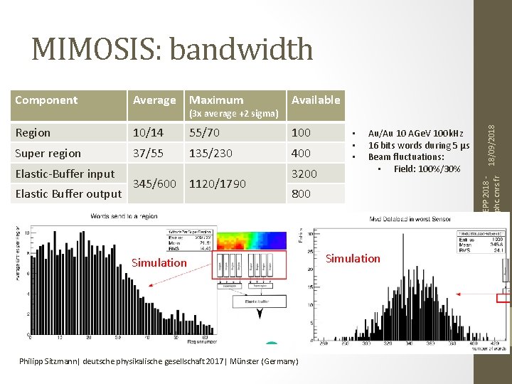
Average Maximum Available Region 10/14 55/70 100 Super region 37/55 135/230 400 Elastic-Buffer input Elastic Buffer output (3 x average +2 sigma) 345/600 1120/1790 3200 • • • Au/Au 10 AGe. V 100 k. Hz 16 bits words during 5 µs Beam fluctuations: • Field: 100%/30% 800 Simulation TWEPP 2018 frederic. morel@iphc. cnrs. fr Component 18/09/2018 MIMOSIS: bandwidth 12 Philipp Sitzmann| deutsche physikalische gesellschaft 2017| Münster (Germany)
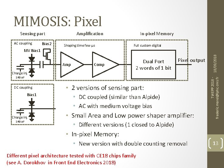
MIMOSIS: Pixel Sensing part AC coupling Bias 2 Amplification Shaping time few µs In-pixel Memory Full custom digital Comp Charge inj. Pixel output 160 a. F DC coupling Bias 1 Charge inj. 160 a. F • 2 versions of sensing part: • DC coupled (similar than Alpide) • AC with medium voltage bias • Small Area and Low power shaper amplifier: TWEPP 2018 frederic. morel@iphc. cnrs. fr Amp Dual Port 2 words of 1 bit 18/09/2018 MV Bias 1 • Different versions (1 closed to Alpide) • In-pixel Memory: • New version with double counting removal Different pixel architecture tested with CE 18 chips family (see A. Dorokhov in Front End Electronics 2018) 13
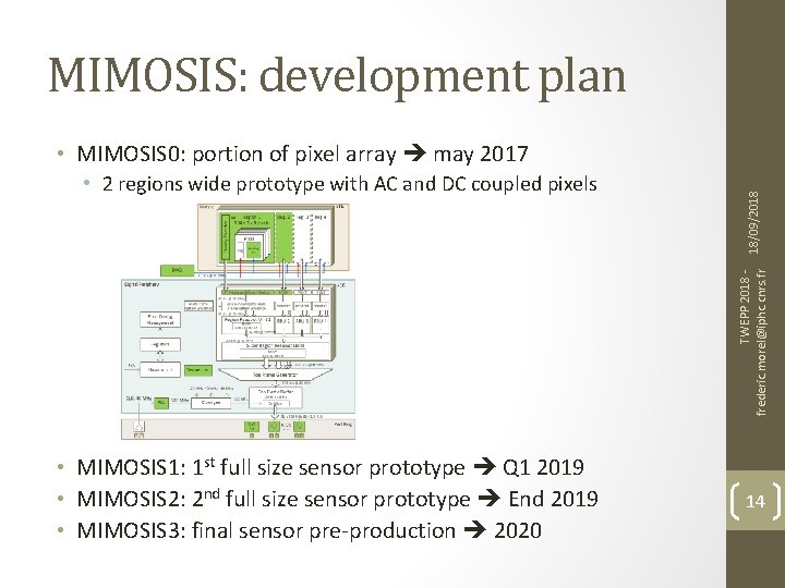
MIMOSIS: development plan TWEPP 2018 frederic. morel@iphc. cnrs. fr • 2 regions wide prototype with AC and DC coupled pixels 18/09/2018 • MIMOSIS 0: portion of pixel array may 2017 • MIMOSIS 1: 1 st full size sensor prototype Q 1 2019 • MIMOSIS 2: 2 nd full size sensor prototype End 2019 • MIMOSIS 3: final sensor pre-production 2020 14
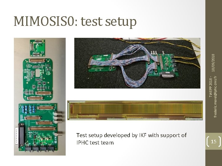
TWEPP 2018 frederic. morel@iphc. cnrs. fr 18/09/2018 MIMOSIS 0: test setup Test setup developed by IKF with support of IPHC test team 15
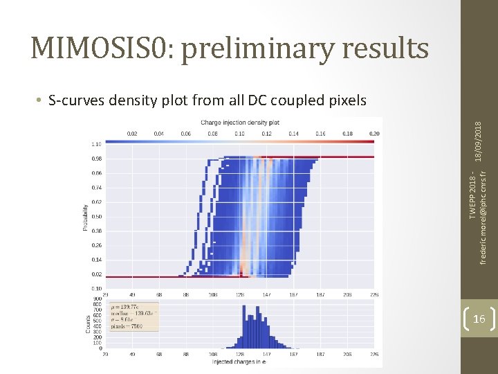
MIMOSIS 0: preliminary results TWEPP 2018 frederic. morel@iphc. cnrs. fr 18/09/2018 • S-curves density plot from all DC coupled pixels 16
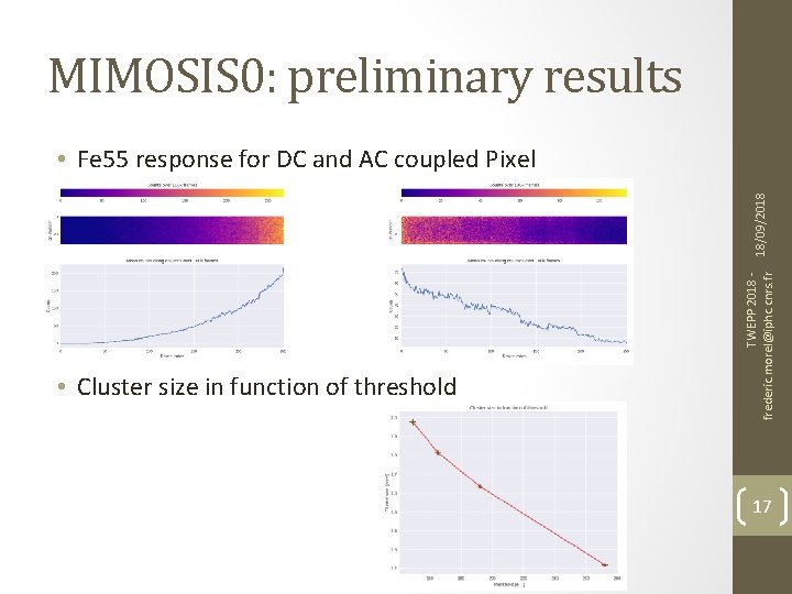
MIMOSIS 0: preliminary results • Cluster size in function of threshold TWEPP 2018 frederic. morel@iphc. cnrs. fr 18/09/2018 • Fe 55 response for DC and AC coupled Pixel 17
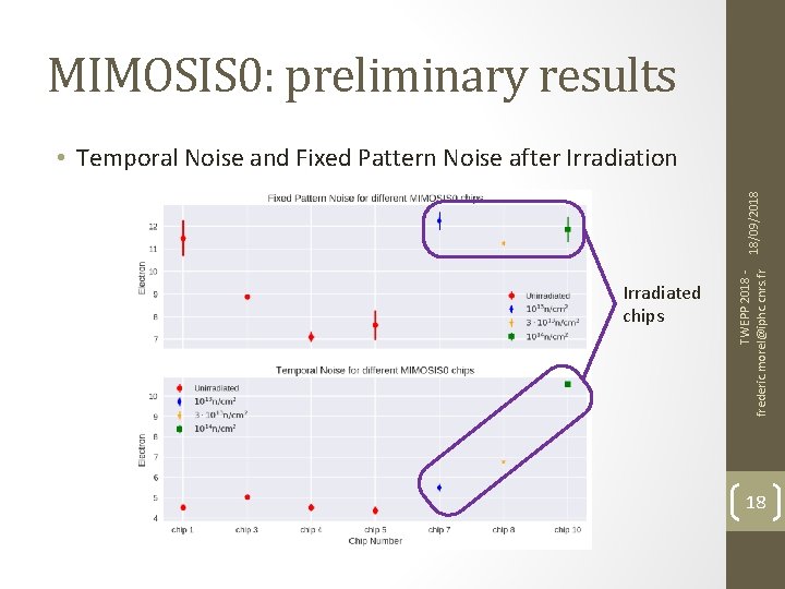
MIMOSIS 0: preliminary results Irradiated chips TWEPP 2018 frederic. morel@iphc. cnrs. fr 18/09/2018 • Temporal Noise and Fixed Pattern Noise after Irradiation 18
• Preliminary results of MIMOSIS 0 are encouraging • AC coupled pixels are promising • Good accordance between tests from MIMOSIS 0 and CE 18 chips family • Design: • MIMOSIS 0 has validated a part of digital readout of MIMOSIS 1 • Digital periphery is under development no showstopper seen • Next steps: • Continuing heavy testing (radiations) of MIMOSIS 0 and CE 18 chips family • Finalize design of MIMOSIS 1 which will be very closed to the final sensors TWEPP 2018 frederic. morel@iphc. cnrs. fr • Close collaboration between IPHC and IKF for tests and design • Tests: 18/09/2018 Conclusion 19
- Slides: 19