Single Cycle CPU Design CS 365 Lecture 7
- Slides: 63
Single Cycle CPU Design CS 365 Lecture 7 Single-cycle CPU CS 365 Spring 2008 GMU
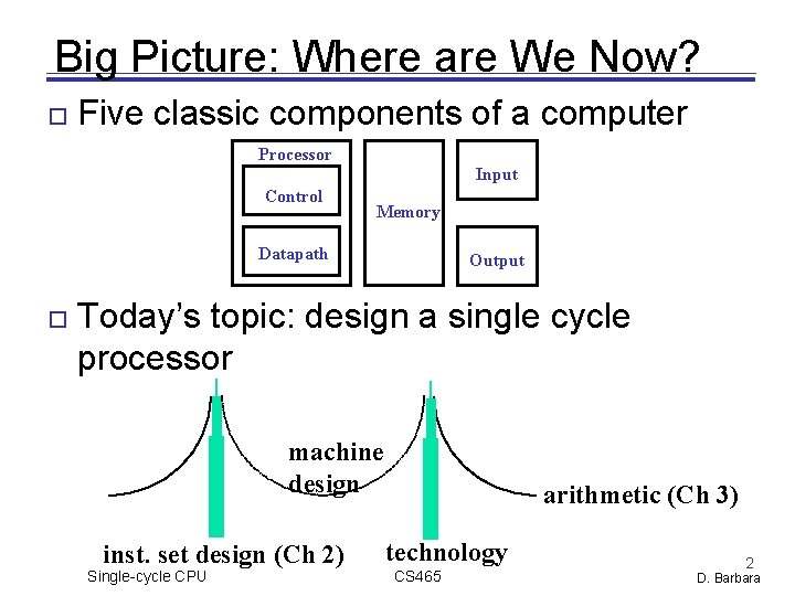
Big Picture: Where are We Now? Five classic components of a computer Processor Input Control Memory Datapath Output Today’s topic: design a single cycle processor machine design inst. set design (Ch 2) Single-cycle CPU arithmetic (Ch 3) technology CS 465 2 D. Barbara
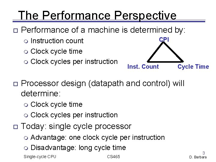
The Performance Perspective Performance of a machine is determined by: Instruction count Clock cycle time Clock cycles per instruction CPI Inst. Count Cycle Time Processor design (datapath and control) will determine: Clock cycle time Clock cycles per instruction Today: single cycle processor Advantage: one clock cycle per instruction Disadvantage: long cycle time Single-cycle CPU CS 465 3 D. Barbara
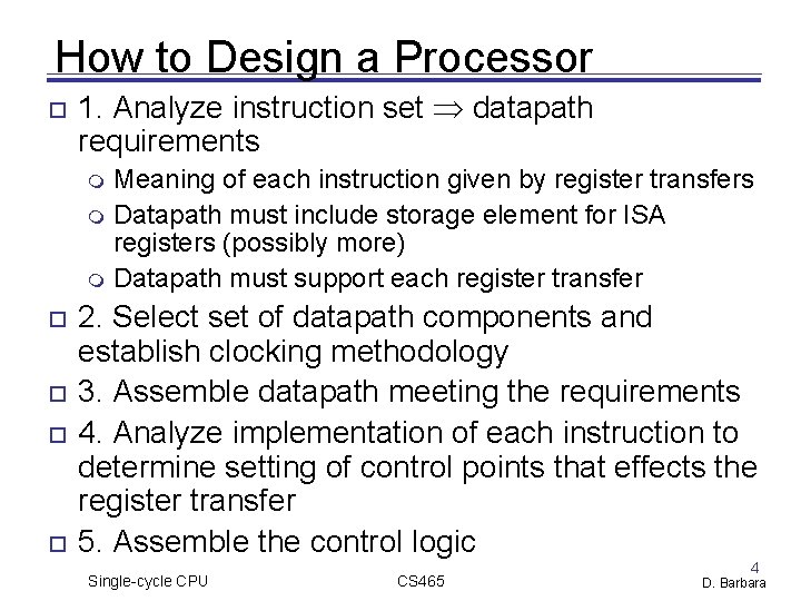
How to Design a Processor 1. Analyze instruction set datapath requirements Meaning of each instruction given by register transfers Datapath must include storage element for ISA registers (possibly more) Datapath must support each register transfer 2. Select set of datapath components and establish clocking methodology 3. Assemble datapath meeting the requirements 4. Analyze implementation of each instruction to determine setting of control points that effects the register transfer 5. Assemble the control logic Single-cycle CPU CS 465 4 D. Barbara
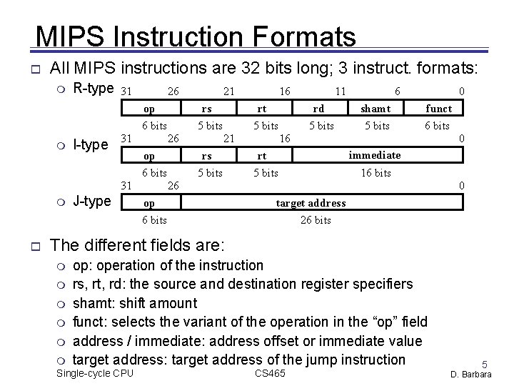
MIPS Instruction Formats All MIPS instructions are 32 bits long; 3 instruct. formats: R-type 31 26 op rs 6 bits I-type 31 op 6 bits J-type 16 rt 5 bits 26 31 21 5 bits 21 rs 5 bits 11 6 0 rd shamt funct 5 bits 6 bits 16 rt 5 bits 0 immediate 16 bits 26 op 6 bits 0 target address 26 bits The different fields are: op: operation of the instruction rs, rt, rd: the source and destination register specifiers shamt: shift amount funct: selects the variant of the operation in the “op” field address / immediate: address offset or immediate value target address: target address of the jump instruction Single-cycle CPU CS 465 5 D. Barbara
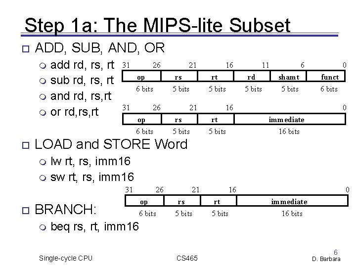
Step 1 a: The MIPS-lite Subset ADD, SUB, AND, OR add rd, rs, rt sub rd, rs, rt and rd, rs, rt or rd, rs, rt 31 26 op 6 bits 31 rs 5 bits 26 op 16 rt 5 bits 21 rs 6 bits 21 rd 5 bits 6 shamt 5 bits 0 funct 6 bits 16 rt 5 bits 11 0 immediate 5 bits 16 bits LOAD and STORE Word lw rt, rs, imm 16 sw rt, rs, imm 16 31 BRANCH: 26 op 6 bits 21 rs 5 bits 16 rt 5 bits 0 immediate 16 bits beq rs, rt, imm 16 Single-cycle CPU CS 465 6 D. Barbara
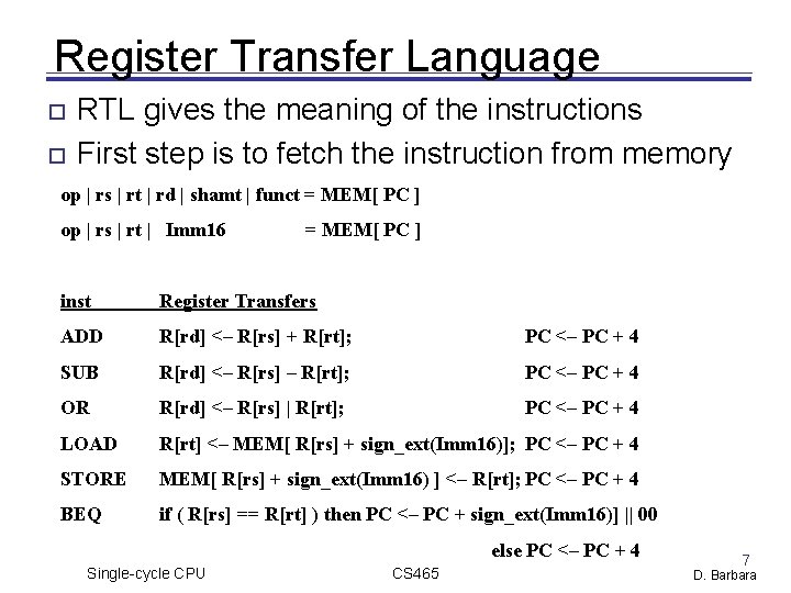
Register Transfer Language RTL gives the meaning of the instructions First step is to fetch the instruction from memory op | rs | rt | rd | shamt | funct = MEM[ PC ] op | rs | rt | Imm 16 = MEM[ PC ] inst Register Transfers ADD R[rd] <– R[rs] + R[rt]; PC <– PC + 4 SUB R[rd] <– R[rs] – R[rt]; PC <– PC + 4 OR R[rd] <– R[rs] | R[rt]; PC <– PC + 4 LOAD R[rt] <– MEM[ R[rs] + sign_ext(Imm 16)]; PC <– PC + 4 STORE MEM[ R[rs] + sign_ext(Imm 16) ] <– R[rt]; PC <– PC + 4 BEQ if ( R[rs] == R[rt] ) then PC <– PC + sign_ext(Imm 16)] || 00 else PC <– PC + 4 Single-cycle CPU CS 465 7 D. Barbara
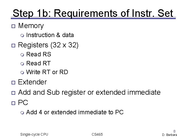
Step 1 b: Requirements of Instr. Set Memory Instruction & data Registers (32 x 32) Read RS Read RT Write RT or RD Extender Add and Sub register or extended immediate PC Add 4 or extended immediate to PC Single-cycle CPU CS 465 8 D. Barbara
Step 2: Components of Datapath Combinational elements Storage elements Clocking Single-cycle CPU methodology CS 465 9 D. Barbara
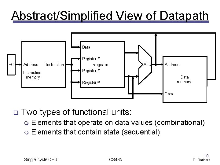
Abstract/Simplified View of Datapath Data PC Address Instruction memory Register # Registers Register # ALU Address Data memory Register # Data Two types of functional units: Elements that operate on data values (combinational) Elements that contain state (sequential) Single-cycle CPU CS 465 10 D. Barbara
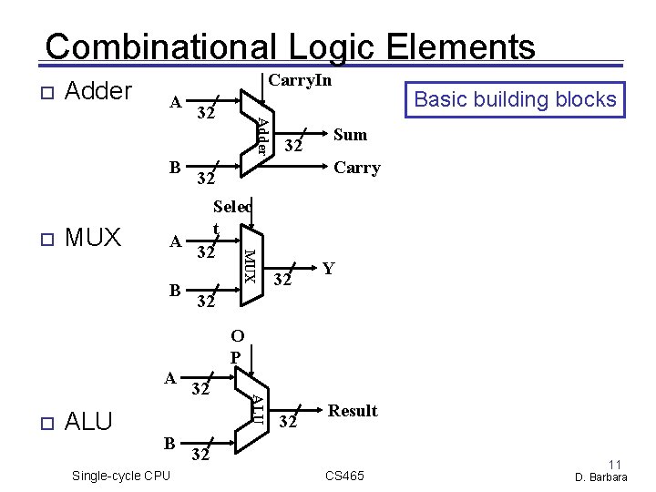
Combinational Logic Elements Adder Carry. In A MUX 32 Selec t A 32 B Basic building blocks Sum Carry 32 MUX Adder B 32 32 Y 32 O P A ALU B Single-cycle CPU ALU 32 32 Result 32 CS 465 11 D. Barbara
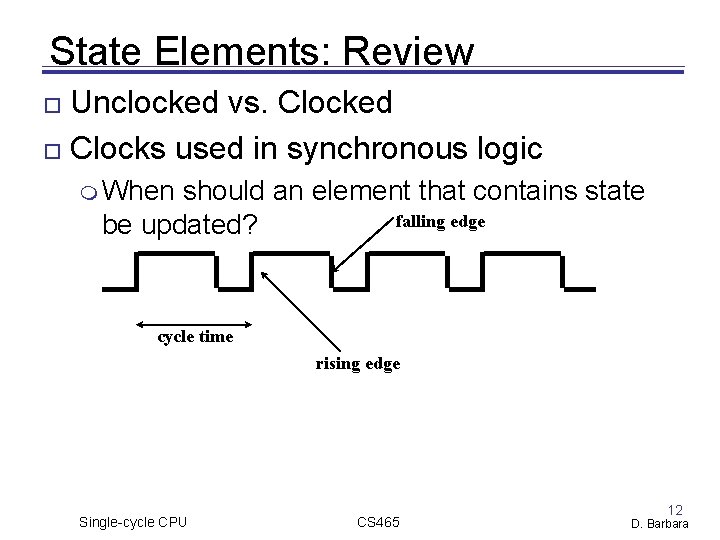
State Elements: Review Unclocked vs. Clocked Clocks used in synchronous logic When should an element that contains state falling edge be updated? cycle time rising edge Single-cycle CPU CS 465 12 D. Barbara
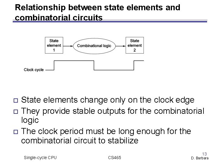
Relationship between state elements and combinatorial circuits State elements change only on the clock edge They provide stable outputs for the combinatorial logic The clock period must be long enough for the combinatorial circuit to stabilize Single-cycle CPU CS 465 13 D. Barbara
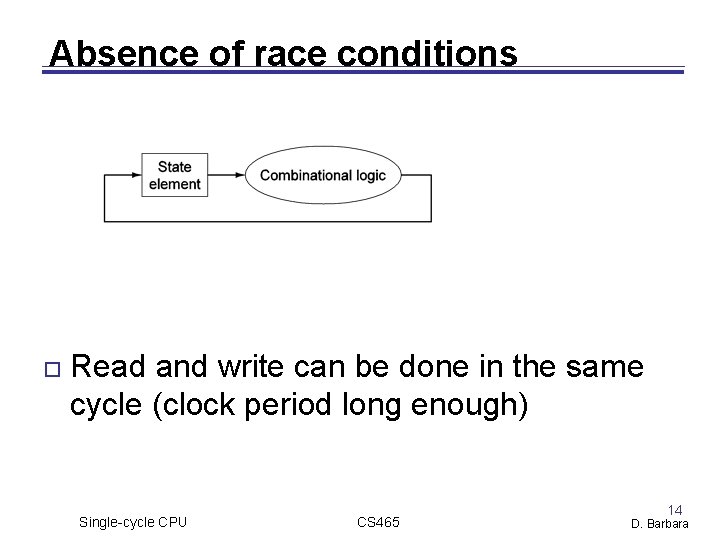
Absence of race conditions Read and write can be done in the same cycle (clock period long enough) Single-cycle CPU CS 465 14 D. Barbara
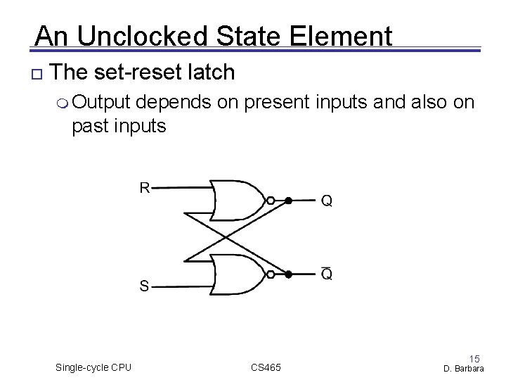
An Unclocked State Element The set-reset latch Output depends on present inputs and also on past inputs Single-cycle CPU CS 465 15 D. Barbara
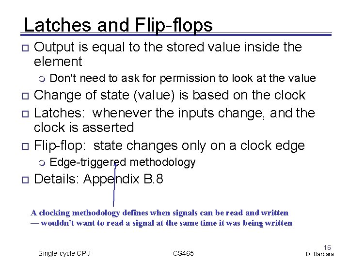
Latches and Flip-flops Output is equal to the stored value inside the element Change of state (value) is based on the clock Latches: whenever the inputs change, and the clock is asserted Flip-flop: state changes only on a clock edge Don't need to ask for permission to look at the value Edge-triggered methodology Details: Appendix B. 8 A clocking methodology defines when signals can be read and written — wouldn't want to read a signal at the same time it was being written Single-cycle CPU CS 465 16 D. Barbara
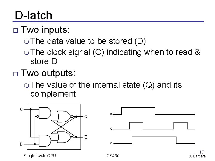
D-latch Two inputs: The data value to be stored (D) The clock signal (C) indicating when to read & store D Two outputs: The value of the internal state (Q) and its complement D C Q Single-cycle CPU CS 465 17 D. Barbara
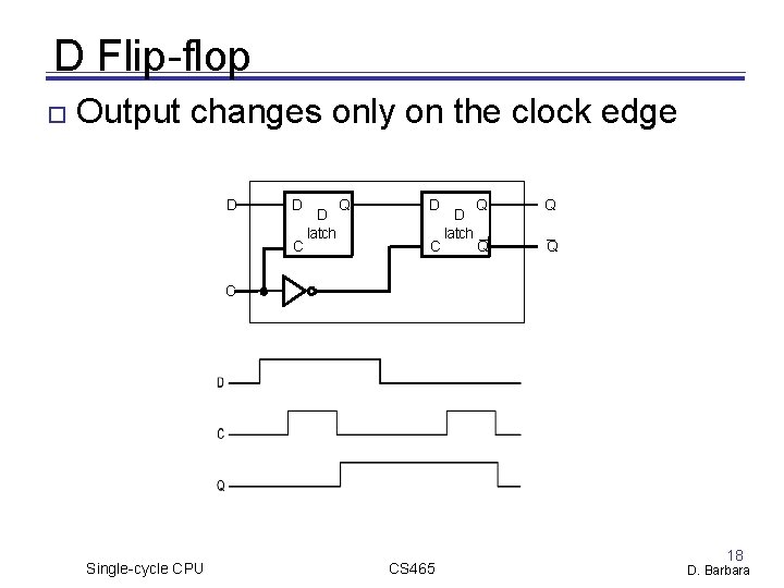
D Flip-flop Output changes only on the clock edge D D C D latch Q D latch _ C Q Q _ Q C Single-cycle CPU CS 465 18 D. Barbara
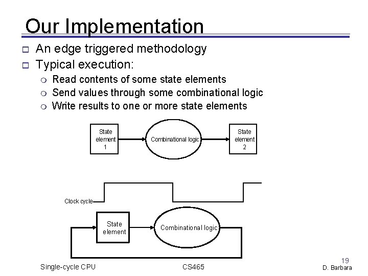
Our Implementation An edge triggered methodology Typical execution: Read contents of some state elements Send values through some combinational logic Write results to one or more state elements State element 1 Combinational logic State element 2 Clock cycle State element Single-cycle CPU Combinational logic CS 465 19 D. Barbara
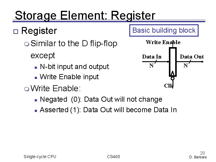
Storage Element: Register Similar Basic building block to the D flip-flop except N-bit input and output Write Enable input Write Enable Data In N Data Out N Clk Enable: Negated (0): Data Out will not change Asserted (1): Data Out will become Data In Single-cycle CPU CS 465 20 D. Barbara
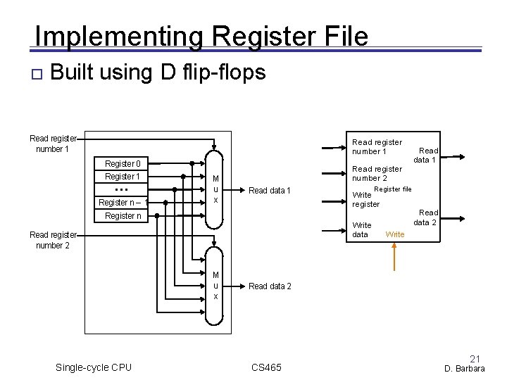
Implementing Register File Built using D flip-flops Read register number 1 Read register nu mber 1 Register 0 Register 1 Register n – 1 M u x Read register nu mber 2 Read data 1 Register file Write register Read data 2 Register n Write data Read register number 2 M u x Single-cycle CPU Read data 1 Write Read data 2 CS 465 21 D. Barbara
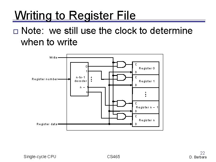
Writing to Register File Note: we still use the clock to determine when to write Write C 0 R egister n u m ber R e gi ster 0 1 D n-to-1 de co der C R e gi ster 1 D n – 1 n C R egister n – 1 D C R e gi ster n D R e gi st er d at a Single-cycle CPU CS 465 22 D. Barbara
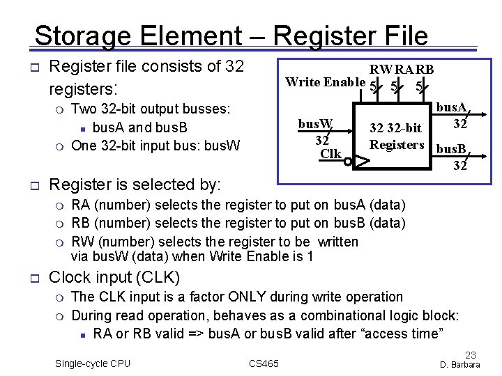
Storage Element – Register File Register file consists of 32 registers: Two 32 -bit output busses: bus. A and bus. B One 32 -bit input bus: bus. W 32 Clk bus. A 32 32 32 -bit Registers bus. B 32 Register is selected by: RWRARB Write Enable 5 5 5 RA (number) selects the register to put on bus. A (data) RB (number) selects the register to put on bus. B (data) RW (number) selects the register to be written via bus. W (data) when Write Enable is 1 Clock input (CLK) The CLK input is a factor ONLY during write operation During read operation, behaves as a combinational logic block: RA or RB valid => bus. A or bus. B valid after “access time” Single-cycle CPU CS 465 23 D. Barbara
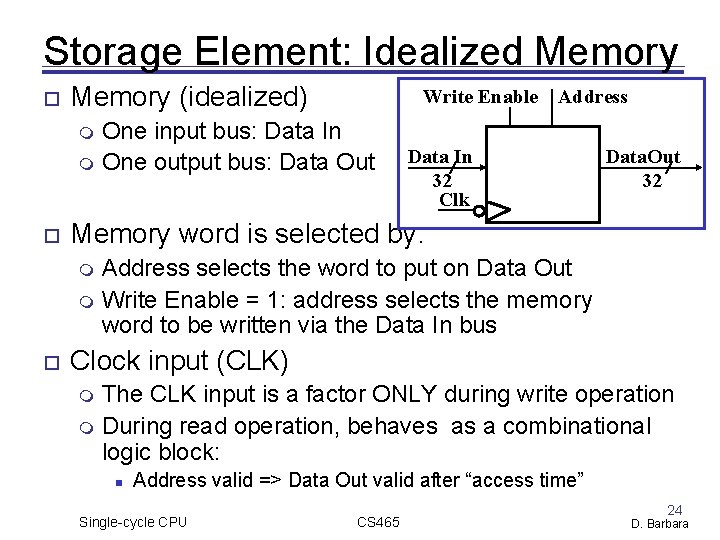
Storage Element: Idealized Memory (idealized) Write Enable Address One input bus: Data In One output bus: Data Out Data In 32 Clk Data. Out 32 Memory word is selected by: Address selects the word to put on Data Out Write Enable = 1: address selects the memory word to be written via the Data In bus Clock input (CLK) The CLK input is a factor ONLY during write operation During read operation, behaves as a combinational logic block: Address valid => Data Out valid after “access time” Single-cycle CPU CS 465 24 D. Barbara
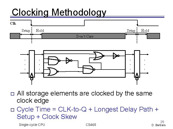
Clocking Methodology Clk Setup Hold . . . Don’t Care . . . All storage elements are clocked by the same clock edge Cycle Time = CLK-to-Q + Longest Delay Path + Setup + Clock Skew Single-cycle CPU CS 465 25 D. Barbara
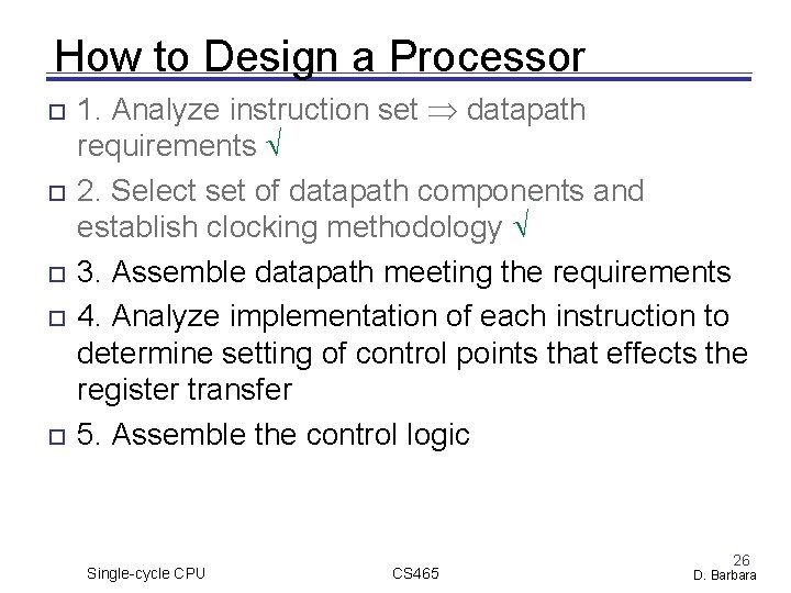
How to Design a Processor 1. Analyze instruction set datapath requirements 2. Select set of datapath components and establish clocking methodology 3. Assemble datapath meeting the requirements 4. Analyze implementation of each instruction to determine setting of control points that effects the register transfer 5. Assemble the control logic Single-cycle CPU CS 465 26 D. Barbara
Step 3 Register transfer requirements Datapath assembly Instruction fetch Read operands and execute operation Single-cycle CPU CS 465 27 D. Barbara
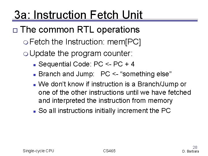
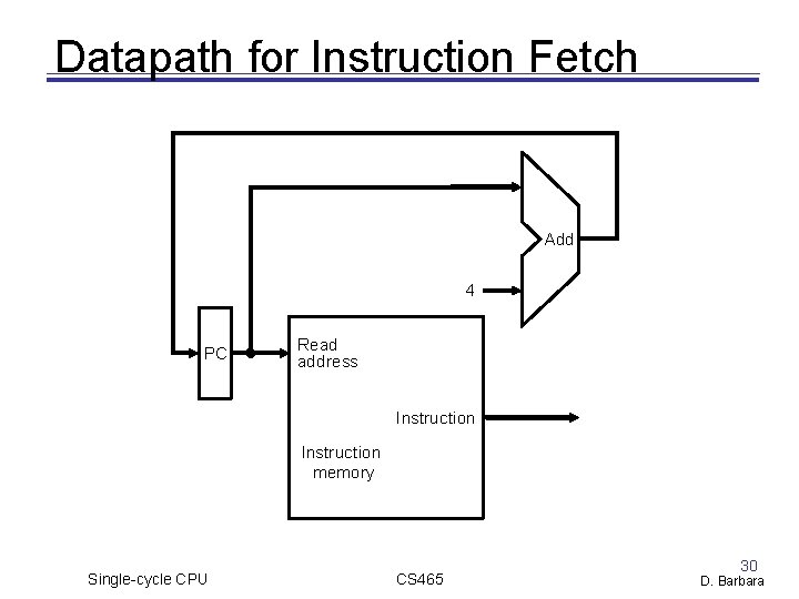
3 a: Instruction Fetch Unit The common RTL operations Fetch the Instruction: mem[PC] Update the program counter: Sequential Code: PC <- PC + 4 Branch and Jump: PC <- “something else” We don’t know if instruction is a Branch/Jump or one of the other instructions until we have fetched and interpreted the instruction from memory So all instructions initially increment the PC Single-cycle CPU CS 465 28 D. Barbara
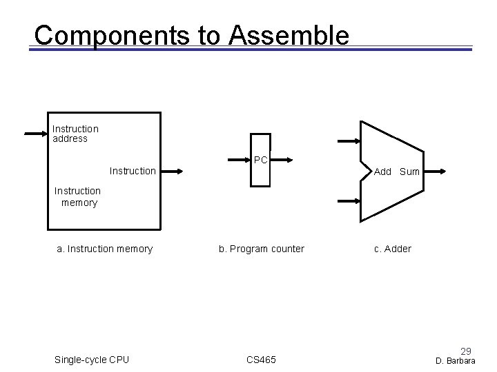
Components to Assemble Instruction address PC Instruction Add Sum Instruction memory a. Instruction memory Single-cycle CPU b. Program counter CS 465 c. Adder 29 D. Barbara
Datapath for Instruction Fetch Add 4 PC Read address Instruction memory Single-cycle CPU CS 465 30 D. Barbara
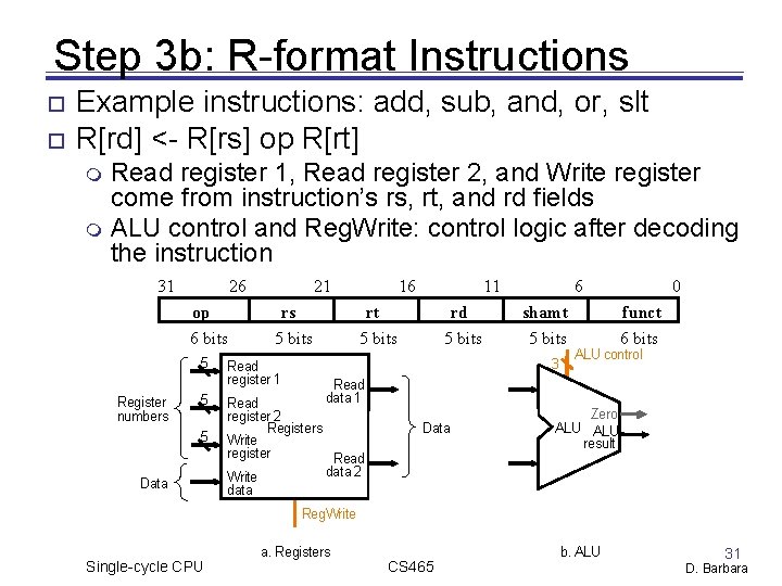
Step 3 b: R-format Instructions Example instructions: add, sub, and, or, slt R[rd] <- R[rs] op R[rt] Read register 1, Read register 2, and Write register come from instruction’s rs, rt, and rd fields ALU control and Reg. Write: control logic after decoding the instruction 31 26 op 6 bits 5 Register numbers 5 5 Data 21 rs 5 bits Read register 1 16 11 rt 5 bits rd 5 bits 6 shamt 5 bits 3 0 funct 6 bits ALU control Read data 1 Read register 2 Registers Write register Read data 2 Write data Data Zero ALU result Reg. Write Single-cycle CPU a. Registers CS 465 b. ALU 31 D. Barbara
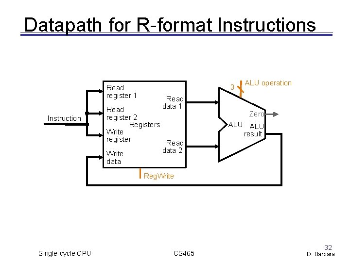
Datapath for R-format Instructions 3 Read register 1 Instruction Read register 2 Registers Write register Write data Read data 1 ALU operation Zero ALU result Read data 2 Reg. Write Single-cycle CPU CS 465 32 D. Barbara
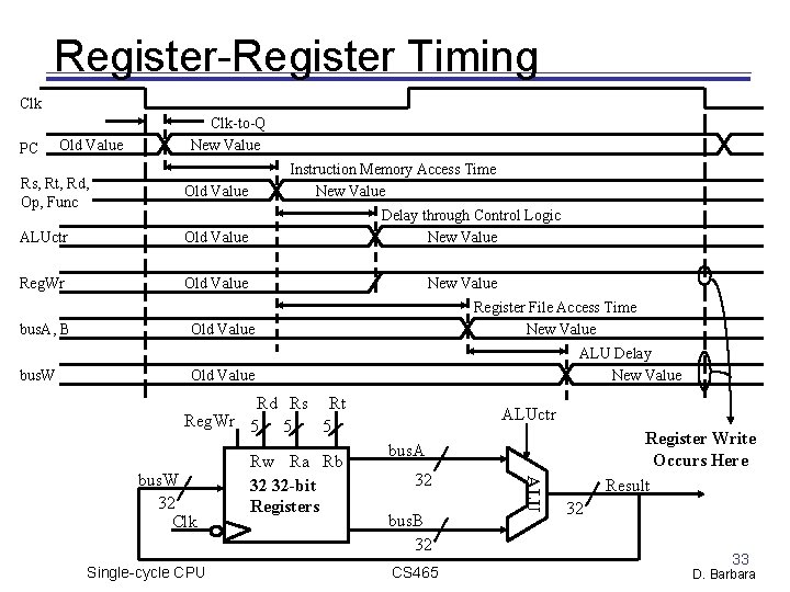
Register-Register Timing Clk PC Old Value Clk-to-Q New Value Rs, Rt, Rd, Op, Func Old Value ALUctr Old Value Reg. Wr Old Value bus. A, B bus. W Instruction Memory Access Time New Value Delay through Control Logic New Value Register File Access Time New Value Old Value ALU Delay New Value Old Value Rd Rs Rt Reg. Wr 5 5 5 Single-cycle CPU Register Write Occurs Here Result bus. A 32 bus. B 32 CS 465 ALU bus. W 32 Clk Rw Ra Rb 32 32 -bit Registers ALUctr 32 33 D. Barbara
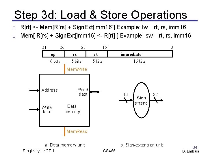
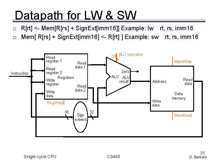
Step 3 d: Load & Store Operations R[rt] <- Mem[R[rs] + Sign. Ext[imm 16]] Example: lw rt, rs, imm 16 Mem[ R[rs] + Sign. Ext[imm 16] <- R[rt] ] Example: sw rt, rs, imm 16 31 26 op 6 bits 21 rs 5 bits 16 rt 5 bits 0 immediate 16 bits Mem. Write Address Write data Read data 16 Data memory Sign extend 32 Mem. Read a. Data memory unit Single-cycle CPU b. Sign-extension unit CS 465 34 D. Barbara
Datapath for LW & SW R[rt] <- Mem[R[rs] + Sign. Ext[imm 16]] Example: lw rt, rs, imm 16 Mem[ R[rs] + Sign. Ext[imm 16] <- R[rt] ] Example: sw rt, rs, imm 16 3 Read register 1 Instruction ALU operation Mem. Write Read data 1 Read register 2 Registers Write register Read data 2 Write data Zero ALU result Write data Reg. Write 16 Single-cycle CPU Address Sign extend 32 Read data Data memory Mem. Read CS 465 35 D. Barbara
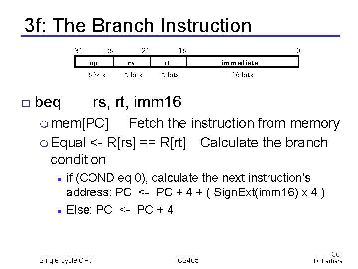
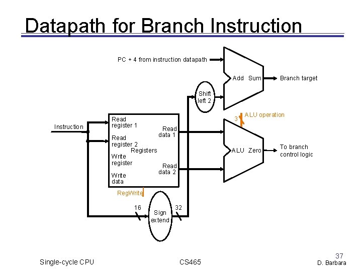
3 f: The Branch Instruction 31 26 op 6 bits beq 21 rs 5 bits 16 rt 5 bits 0 immediate 16 bits rs, rt, imm 16 mem[PC] Fetch the instruction from memory Equal <- R[rs] == R[rt] Calculate the branch condition if (COND eq 0), calculate the next instruction’s address: PC <- PC + 4 + ( Sign. Ext(imm 16) x 4 ) Else: PC <- PC + 4 Single-cycle CPU CS 465 36 D. Barbara
Datapath for Branch Instruction PC + 4 from instruction datapath Add Sum Branch target Shift left 2 Instruction 3 Read register 1 Read register 2 Registers Write register Write data ALU operation Read data 1 ALU Zero To branch control logic Read data 2 Reg. Write 16 Single-cycle CPU Sign extend 32 CS 465 37 D. Barbara
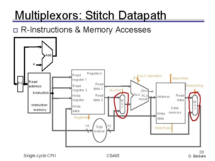
Multiplexors: Stitch Datapath R-Instructions & Memory Accesses Add 4 PC Read addres s Ins truction Instruction memory Read register 1 Registers 3 Read register 2 Read data 1 Write register Read data 2 ALUSrc M u x Zero ALU result Address Write data Reg. Write Single-cycle CPU Mem. Write Memto. Reg Write data 16 ALU operation Sign 32 extend CS 465 Read data Data memory M u x Mem. Read 38 D. Barbara
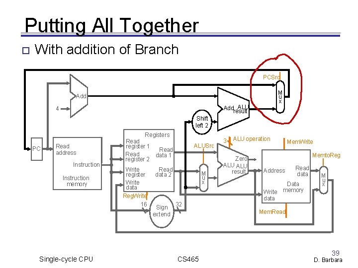
Putting All Together With addition of Branch PCSrc M u x Add ALU result 4 Shift left 2 PC Read address Instruction memory Single-cycle CPU Registers Read register 1 Read data 1 register 2 Write register Write data Reg. Write 16 ALUSrc Read data 2 Sign extend M u x 32 3 ALU operation Zero ALU result Mem. Write Memto. Reg Address Read data Data memory Write data M u x Mem. Read CS 465 39 D. Barbara
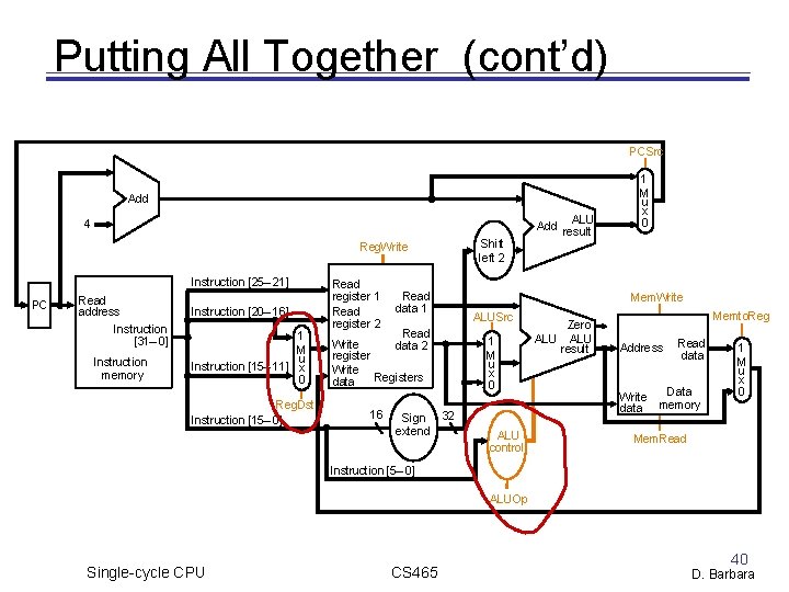
Putting All Together (cont’d) PCSrc Add 4 Reg. Write Instruction [25– 21] PC Read address Instruction [31– 0] Instruction memory Instruction [20– 16] 1 M u Instruction [15– 11] x 0 Reg. Dst Instruction [15– 0] Read register 1 Read register 2 Read data 1 Read Write data 2 register Write Registers data 16 Sign 32 extend Shift left 2 ALU Add result 1 M u x 0 Mem. Write ALUSrc 1 M u x 0 ALU control Zero ALU result Memto. Reg Address Read data Data Write memory data 1 M u x 0 Mem. Read Instruction [5– 0] ALUOp Single-cycle CPU CS 465 40 D. Barbara
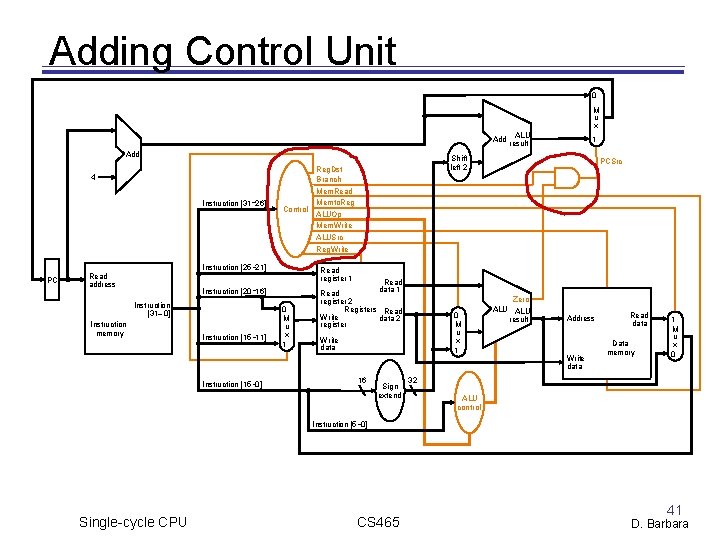
Adding Control Unit 0 M u x ALU Add result Add 4 Instruction [31 26] PC Control Instruction [25 21] Read address Instruction memory Instruction [15 11] Instruction [15 0] Shift left 2 Reg. Dst Branch Mem. Read Memto. Reg ALUOp Mem. Write ALUSrc Reg. Write PCSrc Read register 1 Instruction [20 16] Instruction [31– 0] 1 0 M u x 1 Read data 1 Read register 2 Registers Read Write data 2 register 0 M u x 1 Write data 16 Sign extend Zero ALU result Address Write data Read data Data memory 1 M u x 0 32 ALU control Instruction [5 0] Single-cycle CPU CS 465 41 D. Barbara
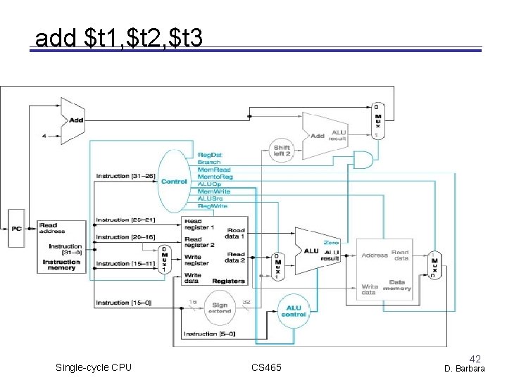
add $t 1, $t 2, $t 3 Single-cycle CPU CS 465 42 D. Barbara
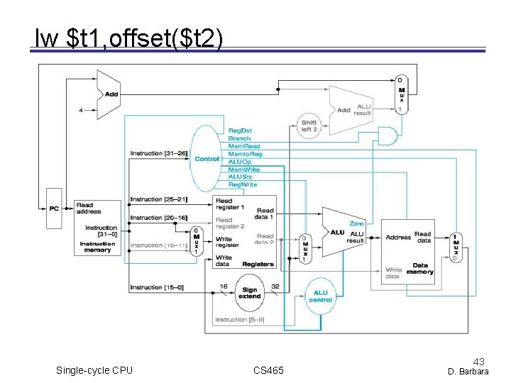
lw $t 1, offset($t 2) Single-cycle CPU CS 465 43 D. Barbara
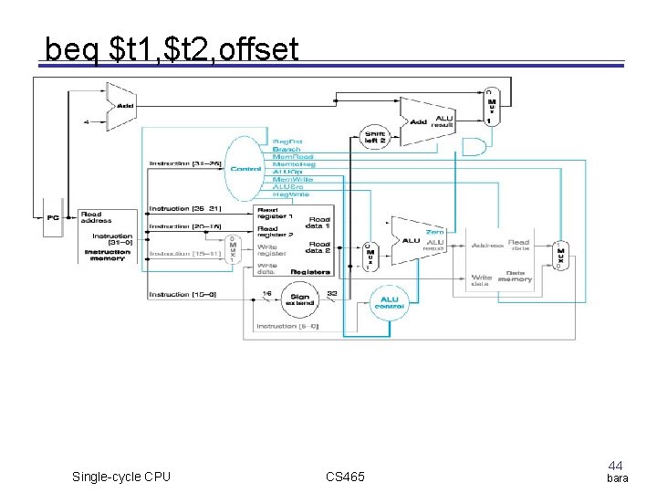
beq $t 1, $t 2, offset Single-cycle CPU CS 465 44 D. Barbara
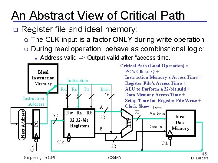
An Abstract View of Critical Path Register file and ideal memory: The CLK input is a factor ONLY during write operation During read operation, behave as combinational logic: Address valid => Output valid after “access time. ” Ideal Instruction Memory Critical Path (Load Operation) = PC’s Clk-to-Q + Instruction Memory’s Access Time + Register File’s Access Time + ALU to Perform a 32 -bit Add + Data Memory Access Time + Setup Time for Register File Write + Clock Skew Data 32 Address Ideal Data In Memory Instruction Rd Rs 5 5 Instruction Address Rt 5 Imm 16 A PC 32 Clk Single-cycle CPU Rw Ra Rb 32 32 -bit Registers 32 ALU Next Address B 32 CS 465 Clk 45 D. Barbara
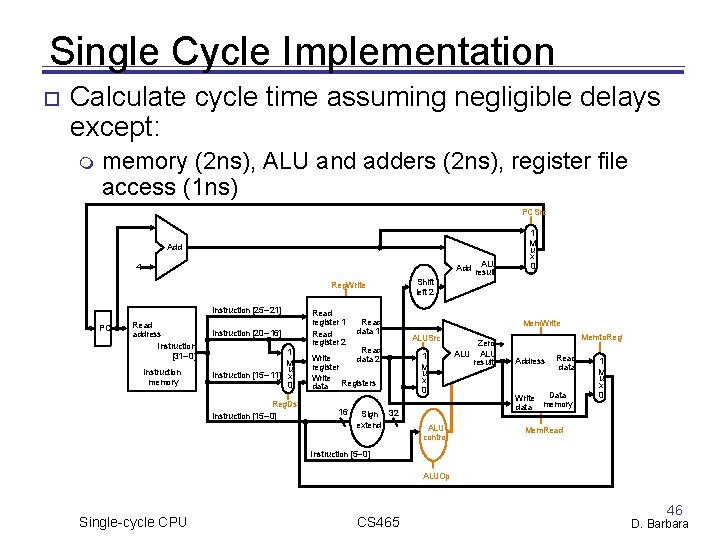
Single Cycle Implementation Calculate cycle time assuming negligible delays except: memory (2 ns), ALU and adders (2 ns), register file access (1 ns) PCSrc Add 4 Reg. Write Instruction [25– 21] PC Read address Instruction [31– 0] Instruction memory Instruction [20– 16] 1 M u Instruction [15– 11] x 0 Reg. Dst Instruction [15– 0] Read register 1 Read register 2 Read data 1 Read Write data 2 register Write data Registers 16 Sign 32 extend Shift left 2 ALU Add result 1 M u x 0 Mem. Write ALUSrc 1 M u x 0 ALU control Zero ALU result Memto. Reg Address Read data Data Write data memory 1 M u x 0 Mem. Read Instruction [5– 0] ALUOp Single-cycle CPU CS 465 46 D. Barbara
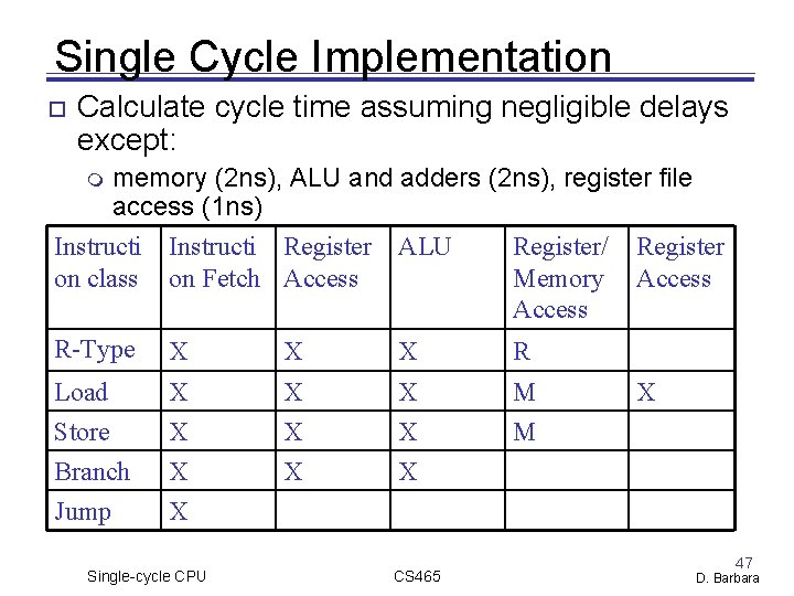
Single Cycle Implementation Calculate cycle time assuming negligible delays except: memory (2 ns), ALU and adders (2 ns), register file access (1 ns) Instructi on class Instructi Register on Fetch Access ALU Register/ Memory Access R-Type X X X R Load Store Branch X X X M M X X X Jump X Single-cycle CPU CS 465 Register Access X 47 D. Barbara
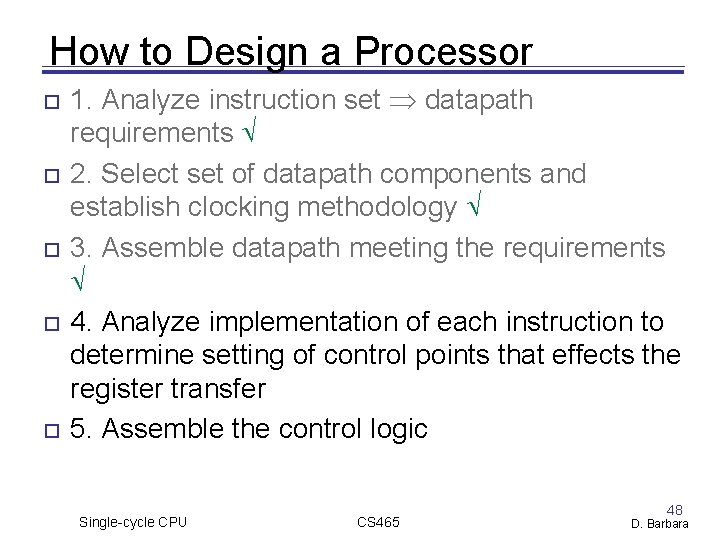
How to Design a Processor 1. Analyze instruction set datapath requirements 2. Select set of datapath components and establish clocking methodology 3. Assemble datapath meeting the requirements 4. Analyze implementation of each instruction to determine setting of control points that effects the register transfer 5. Assemble the control logic Single-cycle CPU CS 465 48 D. Barbara
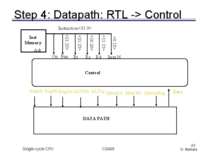
Step 4: Datapath: RTL -> Control Instruction<31: 0> Rs Rd <0: 15> Rt <11: 15> Op Fun <16: 20> Adr <21: 25> Inst Memory Imm 16 Control Branch Reg. Wr Reg. Dst ALUSrc ALUop Mem. Rd Mem. Wr Memto. Reg Zero DATA PATH Single-cycle CPU CS 465 49 D. Barbara
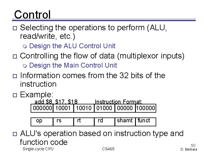
Control Selecting the operations to perform (ALU, read/write, etc. ) Controlling the flow of data (multiplexor inputs) Design the ALU Control Unit Design the Main Control Unit Information comes from the 32 bits of the instruction Example: add $8, $17, $18 Instruction Format: 000000 10001 10010 01000 00000 100000 op rs rt rd shamt funct ALU's operation based on instruction type and function code Single-cycle CPU CS 465 50 D. Barbara
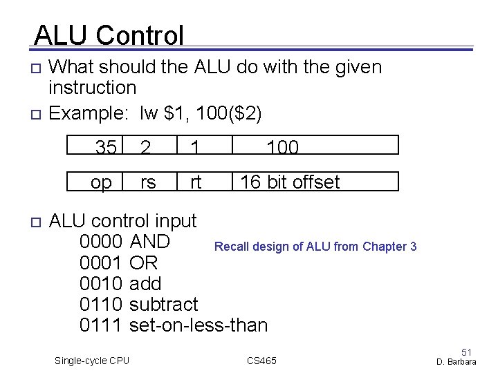
ALU Control What should the ALU do with the given instruction Example: lw $1, 100($2) 35 2 1 op rs rt 100 16 bit offset ALU control input 0000 AND Recall design of ALU from Chapter 3 0001 OR 0010 add 0110 subtract 0111 set-on-less-than Single-cycle CPU CS 465 51 D. Barbara
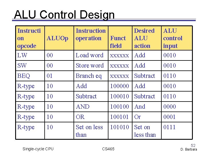
ALU Control Design Instructi on ALUOp opcode Instruction operation Funct field LW 00 Load word xxxxxx Add 0010 SW 00 Store word xxxxxx Add 0010 BEQ 01 Branch eq xxxxxx Subtract 0110 R-type 10 Add 100000 Add 0010 R-type 10 Subtract 100010 Subtract 0110 R-type 10 AND 100100 And 0000 R-type 10 OR 100101 Or 0001 R-type 10 Set on less than 101010 Set on less than 0111 Single-cycle CPU CS 465 Desired ALU action ALU control input 52 D. Barbara
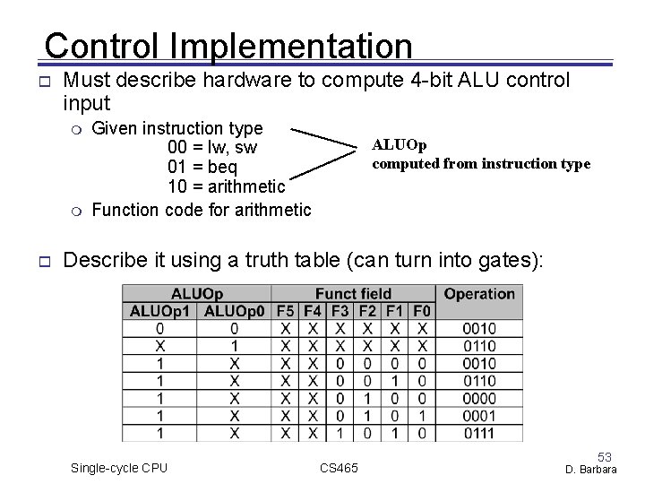
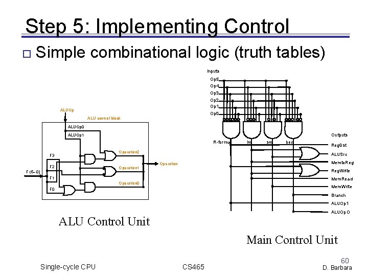
Control Implementation Must describe hardware to compute 4 -bit ALU control input Given instruction type 00 = lw, sw 01 = beq 10 = arithmetic Function code for arithmetic ALUOp computed from instruction type Describe it using a truth table (can turn into gates): Single-cycle CPU CS 465 53 D. Barbara
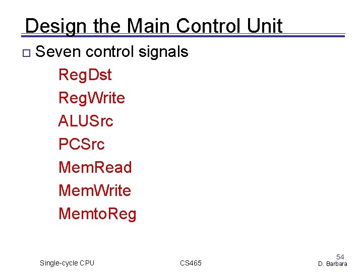
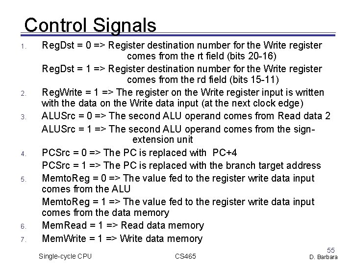
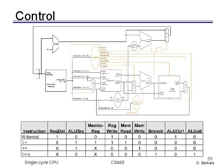
Design the Main Control Unit Seven control signals Reg. Dst Reg. Write ALUSrc PCSrc Mem. Read Mem. Write Memto. Reg Single-cycle CPU CS 465 54 D. Barbara
Control Signals 1. 2. 3. 4. 5. 6. 7. Reg. Dst = 0 => Register destination number for the Write register comes from the rt field (bits 20 -16) Reg. Dst = 1 => Register destination number for the Write register comes from the rd field (bits 15 -11) Reg. Write = 1 => The register on the Write register input is written with the data on the Write data input (at the next clock edge) ALUSrc = 0 => The second ALU operand comes from Read data 2 ALUSrc = 1 => The second ALU operand comes from the signextension unit PCSrc = 0 => The PC is replaced with PC+4 PCSrc = 1 => The PC is replaced with the branch target address Memto. Reg = 0 => The value fed to the register write data input comes from the ALU Memto. Reg = 1 => The value fed to the register write data input comes from the data memory Mem. Read = 1 => Read data memory Mem. Write = 1 => Write data memory Single-cycle CPU CS 465 55 D. Barbara
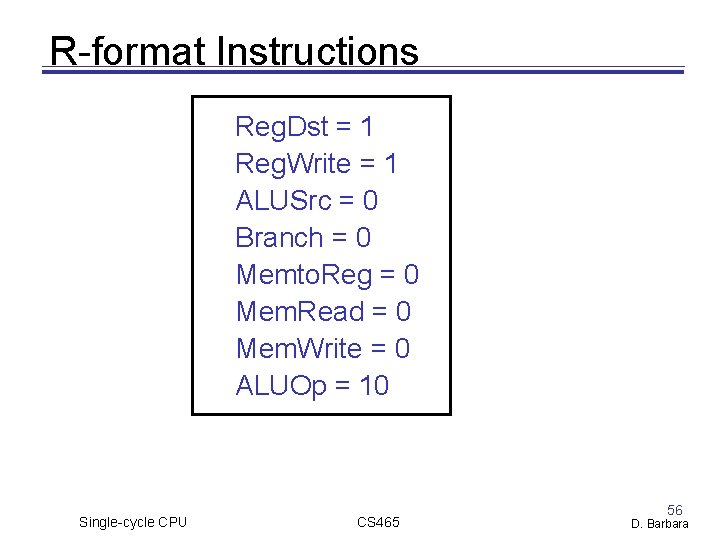
R-format Instructions Reg. Dst = 1 Reg. Write = 1 ALUSrc = 0 Branch = 0 Memto. Reg = 0 Mem. Read = 0 Mem. Write = 0 ALUOp = 10 Single-cycle CPU CS 465 56 D. Barbara
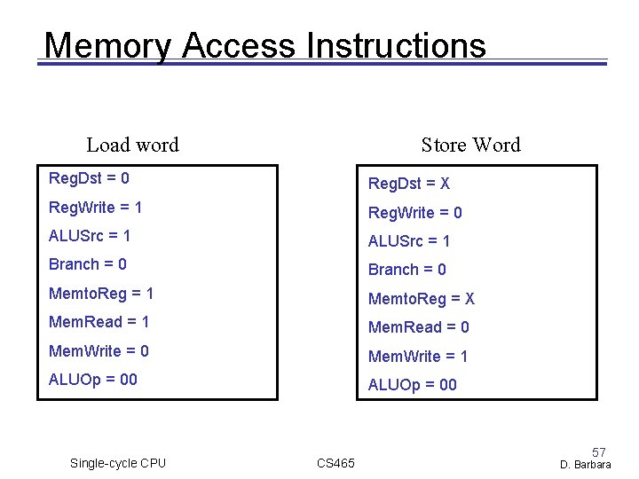
Memory Access Instructions Load word Store Word Reg. Dst = 0 Reg. Dst = X Reg. Write = 1 Reg. Write = 0 ALUSrc = 1 Branch = 0 Memto. Reg = 1 Memto. Reg = X Mem. Read = 1 Mem. Read = 0 Mem. Write = 1 ALUOp = 00 Single-cycle CPU CS 465 57 D. Barbara
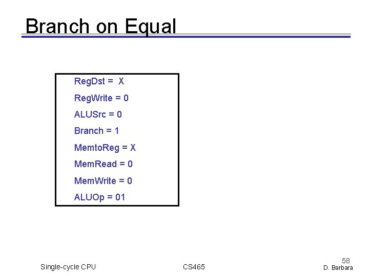
Branch on Equal Reg. Dst = X Reg. Write = 0 ALUSrc = 0 Branch = 1 Memto. Reg = X Mem. Read = 0 Mem. Write = 0 ALUOp = 01 Single-cycle CPU CS 465 58 D. Barbara
Control Single-cycle CPU CS 465 59 D. Barbara
Step 5: Implementing Control Simple combinational logic (truth tables) Inputs Op 5 Op 4 Op 3 Op 2 Op 1 ALUOp Op 0 ALU control block ALUOp 0 Outputs ALUOp 1 R-format Operation 2 F 3 F 2 Operation 1 F (5– 0) Iw sw beq Reg. Dst ALUSrc Memto. Reg Operation Reg. Write F 1 Mem. Read Operation 0 Mem. Write F 0 Branch ALUOp 1 ALUOp. O ALU Control Unit Main Control Unit Single-cycle CPU CS 465 60 D. Barbara
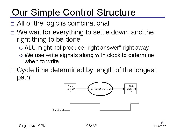
Our Simple Control Structure All of the logic is combinational We wait for everything to settle down, and the right thing to be done ALU might not produce “right answer” right away We use write signals along with clock to determine when to write Cycle time determined by length of the longest path State ele ment 1 Co mbinational logic State element 2 Clock cycle Single-cycle CPU CS 465 61 D. Barbara
Summary 5 steps to design a processor MIPS makes it easier 1. Analyze instruction set => datapath requirements 2. Select set of datapath components & establish clock methodology 3. Assemble datapath meeting the requirements 4. Analyze implementation of each instruction to determine setting of control points that effects the register transfer 5. Assemble the control logic Instructions same size Source registers always in same place Immediates same size, location Operations always on registers/immediates Single cycle datapath => CPI=1, Clock Cycle Time => long Single-cycle CPU CS 465 62 D. Barbara
Next Lecture Topic: Multiple cycle implementation of CPU Reading Ch 5 Patterson and Hennessy Single-cycle CPU CS 465 63 D. Barbara