PLASMA ATOMIC LAYER ETCHING Ankur Agarwala and Mark
- Slides: 24

PLASMA ATOMIC LAYER ETCHING* Ankur Agarwala) and Mark J. Kushnerb) a)Department of Chemical and Biomolecular Engineering University of Illinois, Urbana, IL 61801, USA Email: aagarwl 3@uiuc. edu b)Department of Electrical and Computer Engineering Iowa State Universit, Ames, IA 50011, USA Email: mjk@iastate. edu http: //uigelz. ece. iastate. edu 33 rd IEEE ICOPS, June 2006 * Work supported by the SRC and NSF

AGENDA · Atomic Layer Processing · Plasma Atomic Layer Etching (PALE) · Approach and Methodology · Demonstration Systems · Results · PALE of Si using Ar/Cl 2 · PALE of Si. O 2 using Ar/c-C 4 F 8 · Concluding Remarks ANKUR_ICOPS 06_Agenda Iowa State University Optical and Discharge Physics

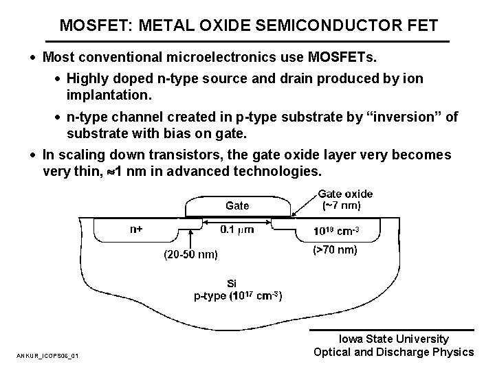
MOSFET: METAL OXIDE SEMICONDUCTOR FET · Most conventional microelectronics use MOSFETs. · Highly doped n-type source and drain produced by ion implantation. · n-type channel created in p-type substrate by “inversion” of substrate with bias on gate. · In scaling down transistors, the gate oxide layer very becomes very thin, 1 nm in advanced technologies. ANKUR_ICOPS 06_01 Iowa State University Optical and Discharge Physics

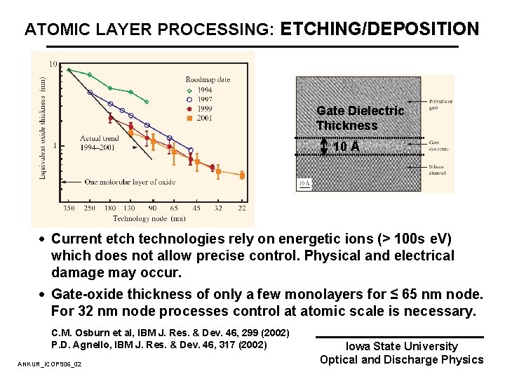
ATOMIC LAYER PROCESSING: ETCHING/DEPOSITION Gate Dielectric Thickness 10 Å · Current etch technologies rely on energetic ions (> 100 s e. V) which does not allow precise control. Physical and electrical damage may occur. · Gate-oxide thickness of only a few monolayers for ≤ 65 nm node. For 32 nm node processes control at atomic scale is necessary. C. M. Osburn et al, IBM J. Res. & Dev. 46, 299 (2002) P. D. Agnello, IBM J. Res. & Dev. 46, 317 (2002) ANKUR_ICOPS 06_02 Iowa State University Optical and Discharge Physics

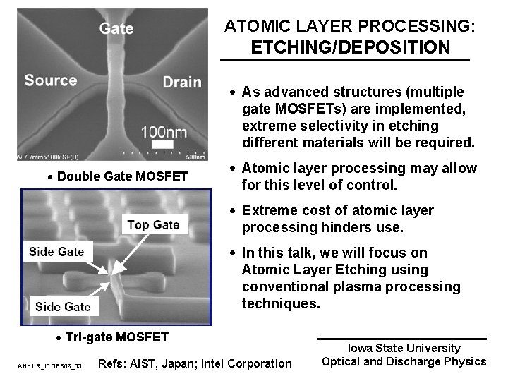
ATOMIC LAYER PROCESSING: ETCHING/DEPOSITION · As advanced structures (multiple gate MOSFETs) are implemented, extreme selectivity in etching different materials will be required. · Double Gate MOSFET · Atomic layer processing may allow for this level of control. · Extreme cost of atomic layer processing hinders use. · In this talk, we will focus on Atomic Layer Etching using conventional plasma processing techniques. · Tri-gate MOSFET ANKUR_ICOPS 06_03 Refs: AIST, Japan; Intel Corporation Iowa State University Optical and Discharge Physics

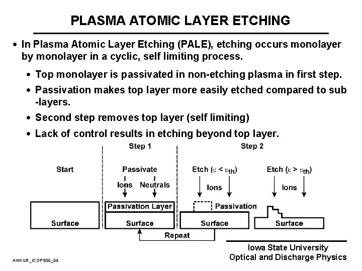
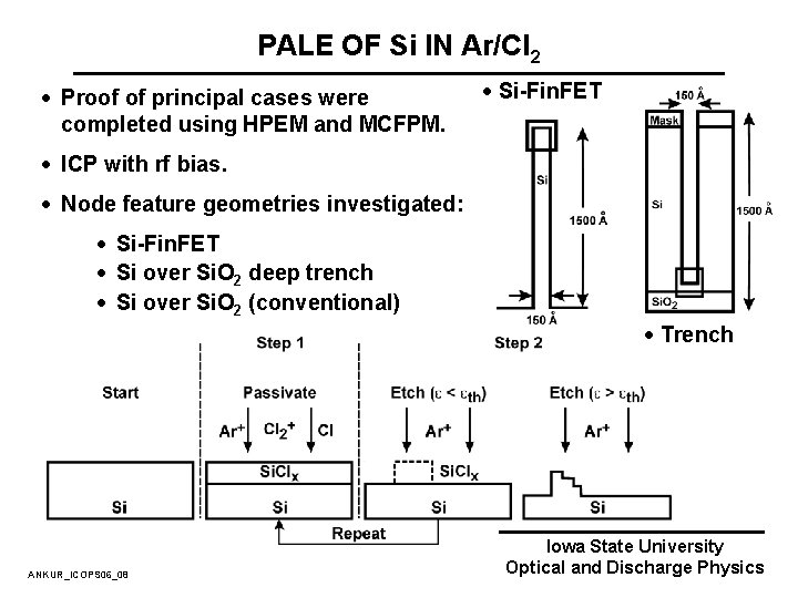
PLASMA ATOMIC LAYER ETCHING · In Plasma Atomic Layer Etching (PALE), etching occurs monolayer by monolayer in a cyclic, self limiting process. · Top monolayer is passivated in non-etching plasma in first step. · Passivation makes top layer more easily etched compared to sub -layers. · Second step removes top layer (self limiting) · Lack of control results in etching beyond top layer. ANKUR_ICOPS 06_04 Iowa State University Optical and Discharge Physics

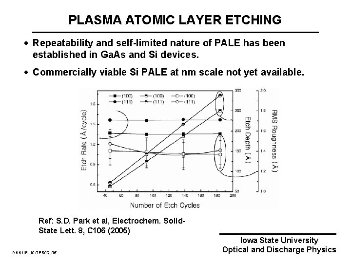
PLASMA ATOMIC LAYER ETCHING · Repeatability and self-limited nature of PALE has been established in Ga. As and Si devices. · Commercially viable Si PALE at nm scale not yet available. Ref: S. D. Park et al, Electrochem. Solid. State Lett. 8, C 106 (2005) ANKUR_ICOPS 06_05 Iowa State University Optical and Discharge Physics

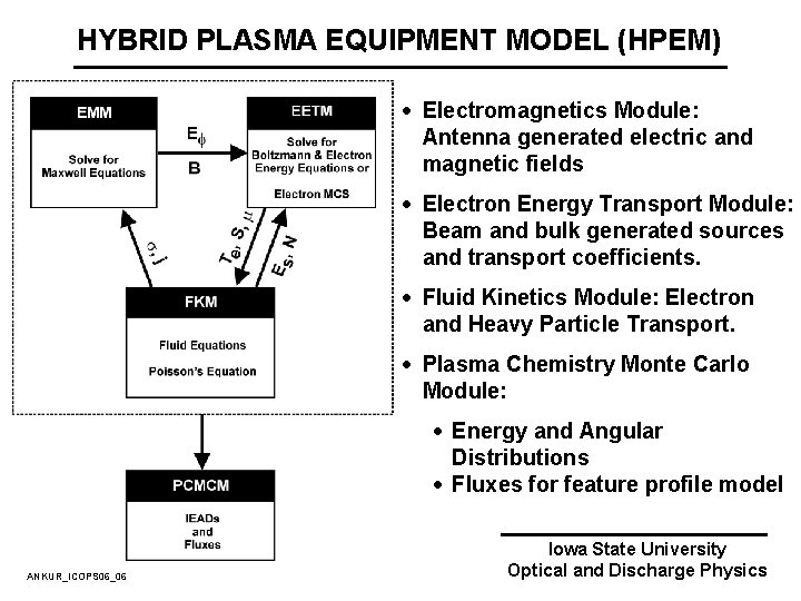
HYBRID PLASMA EQUIPMENT MODEL (HPEM) · Electromagnetics Module: Antenna generated electric and magnetic fields · Electron Energy Transport Module: Beam and bulk generated sources and transport coefficients. · Fluid Kinetics Module: Electron and Heavy Particle Transport. · Plasma Chemistry Monte Carlo Module: · Energy and Angular Distributions · Fluxes for feature profile model ANKUR_ICOPS 06_06 Iowa State University Optical and Discharge Physics

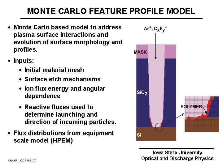
MONTE CARLO FEATURE PROFILE MODEL · Monte Carlo based model to address plasma surface interactions and evolution of surface morphology and profiles. · Inputs: · Initial material mesh · Surface etch mechanisms · Ion flux energy and angular dependence · Reactive fluxes used to determine launching and direction of incoming particles. · Flux distributions from equipment scale model (HPEM) ANKUR_ICOPS 06_07 Iowa State University Optical and Discharge Physics

PALE OF Si IN Ar/Cl 2 · Proof of principal cases were completed using HPEM and MCFPM. · Si-Fin. FET · ICP with rf bias. · Node feature geometries investigated: · Si-Fin. FET · Si over Si. O 2 deep trench · Si over Si. O 2 (conventional) · Trench ANKUR_ICOPS 06_08 Iowa State University Optical and Discharge Physics

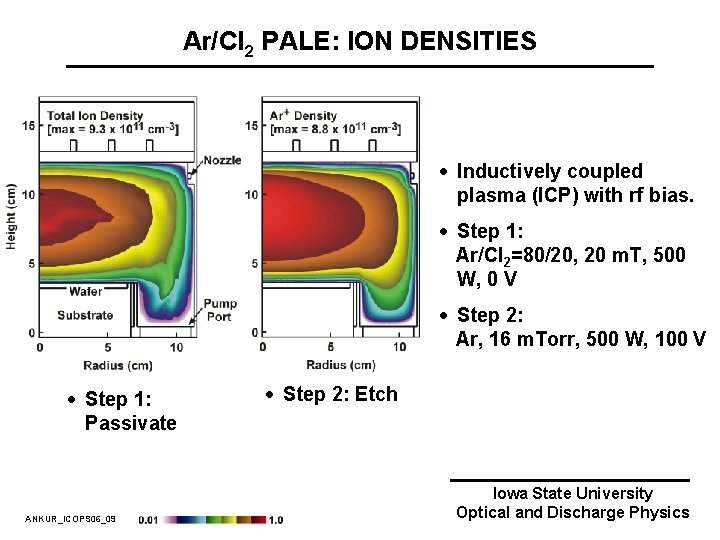
Ar/Cl 2 PALE: ION DENSITIES · Inductively coupled plasma (ICP) with rf bias. · Step 1: Ar/Cl 2=80/20, 20 m. T, 500 W, 0 V · Step 2: Ar, 16 m. Torr, 500 W, 100 V · Step 1: Passivate ANKUR_ICOPS 06_09 · Step 2: Etch Iowa State University Optical and Discharge Physics

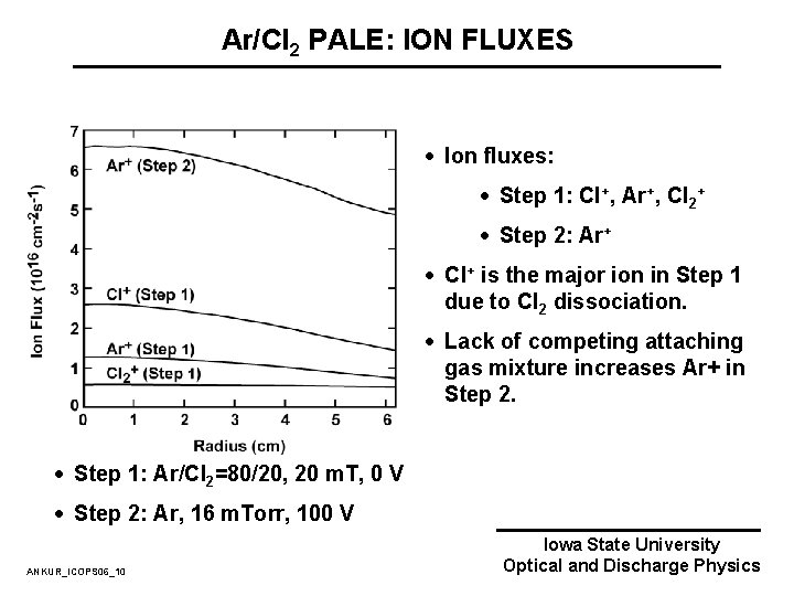
Ar/Cl 2 PALE: ION FLUXES · Ion fluxes: · Step 1: Cl+, Ar+, Cl 2+ · Step 2: Ar+ · Cl+ is the major ion in Step 1 due to Cl 2 dissociation. · Lack of competing attaching gas mixture increases Ar+ in Step 2. · Step 1: Ar/Cl 2=80/20, 20 m. T, 0 V · Step 2: Ar, 16 m. Torr, 100 V ANKUR_ICOPS 06_10 Iowa State University Optical and Discharge Physics

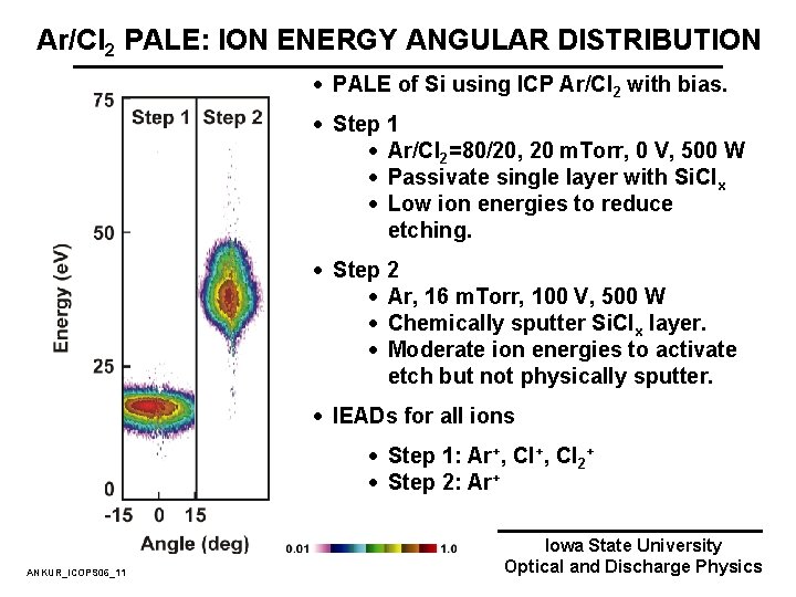
Ar/Cl 2 PALE: ION ENERGY ANGULAR DISTRIBUTION · PALE of Si using ICP Ar/Cl 2 with bias. · Step 1 · Ar/Cl 2=80/20, 20 m. Torr, 0 V, 500 W · Passivate single layer with Si. Clx · Low ion energies to reduce etching. · Step 2 · Ar, 16 m. Torr, 100 V, 500 W · Chemically sputter Si. Clx layer. · Moderate ion energies to activate etch but not physically sputter. · IEADs for all ions · Step 1: Ar+, Cl 2+ · Step 2: Ar+ ANKUR_ICOPS 06_11 Iowa State University Optical and Discharge Physics

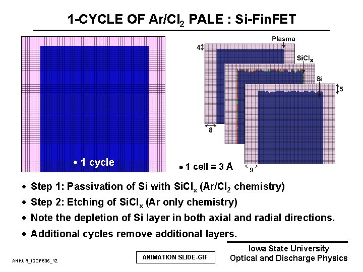
1 -CYCLE OF Ar/Cl 2 PALE : Si-Fin. FET · 1 cycle 1 cell = 3 Å · Step 1: Passivation of Si with Si. Clx (Ar/Cl 2 chemistry) · Step 2: Etching of Si. Clx (Ar only chemistry) · Note the depletion of Si layer in both axial and radial directions. · Additional cycles remove additional layers. ANKUR_ICOPS 06_12 ANIMATION SLIDE-GIF Iowa State University Optical and Discharge Physics

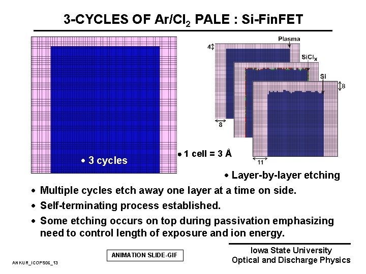
3 -CYCLES OF Ar/Cl 2 PALE : Si-Fin. FET · 3 cycles 1 cell = 3 Å · Layer-by-layer etching · Multiple cycles etch away one layer at a time on side. · Self-terminating process established. · Some etching occurs on top during passivation emphasizing need to control length of exposure and ion energy. ANIMATION SLIDE-GIF ANKUR_ICOPS 06_13 Iowa State University Optical and Discharge Physics

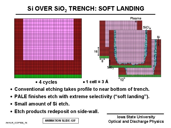
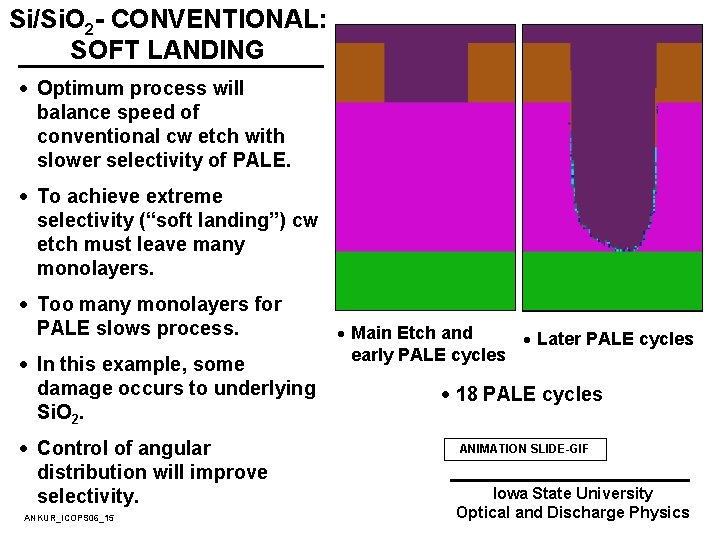
Si OVER Si. O 2 TRENCH: SOFT LANDING Si. O 2 1 cell = 3 Å · 4 cycles · Conventional etching takes profile to near bottom of trench. · PALE finishes etch with extreme selectivity (“soft landing”). · Small amount of Si etch. · Etch products redeposit on side-wall. ANKUR_ICOPS 06_14 ANIMATION SLIDE-GIF Iowa State University Optical and Discharge Physics

Si/Si. O 2 - CONVENTIONAL: SOFT LANDING · Optimum process will balance speed of conventional cw etch with slower selectivity of PALE. · To achieve extreme selectivity (“soft landing”) cw etch must leave many monolayers. · Too many monolayers for PALE slows process. · In this example, some damage occurs to underlying Si. O 2. · Control of angular distribution will improve selectivity. ANKUR_ICOPS 06_15 · Main Etch and · Later PALE cycles early PALE cycles · 18 PALE cycles ANIMATION SLIDE-GIF Iowa State University Optical and Discharge Physics

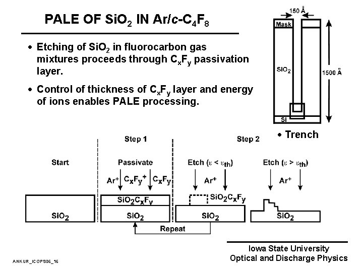
PALE OF Si. O 2 IN Ar/c-C 4 F 8 · Etching of Si. O 2 in fluorocarbon gas mixtures proceeds through Cx. Fy passivation layer. · Control of thickness of Cx. Fy layer and energy of ions enables PALE processing. · Trench ANKUR_ICOPS 06_16 Iowa State University Optical and Discharge Physics

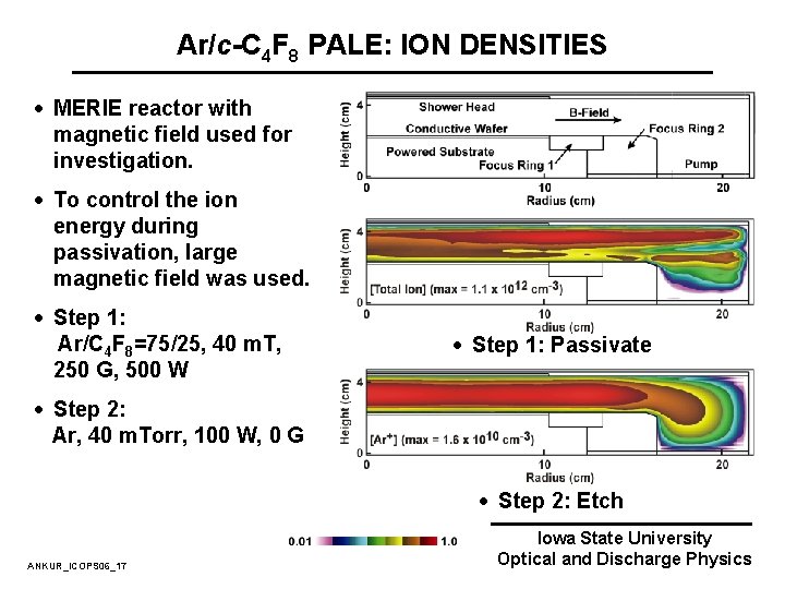
Ar/c-C 4 F 8 PALE: ION DENSITIES · MERIE reactor with magnetic field used for investigation. · To control the ion energy during passivation, large magnetic field was used. · Step 1: Ar/C 4 F 8=75/25, 40 m. T, 250 G, 500 W · Step 1: Passivate · Step 2: Ar, 40 m. Torr, 100 W, 0 G · Step 2: Etch ANKUR_ICOPS 06_17 Iowa State University Optical and Discharge Physics

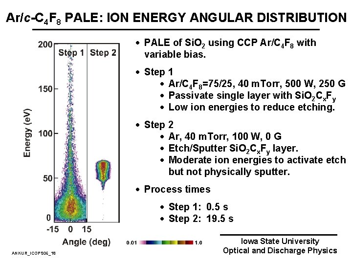
Ar/c-C 4 F 8 PALE: ION ENERGY ANGULAR DISTRIBUTION · PALE of Si. O 2 using CCP Ar/C 4 F 8 with variable bias. · Step 1 · Ar/C 4 F 8=75/25, 40 m. Torr, 500 W, 250 G · Passivate single layer with Si. O 2 Cx. Fy · Low ion energies to reduce etching. · Step 2 · Ar, 40 m. Torr, 100 W, 0 G · Etch/Sputter Si. O 2 Cx. Fy layer. · Moderate ion energies to activate etch but not physically sputter. · Process times · Step 1: 0. 5 s · Step 2: 19. 5 s ANKUR_ICOPS 06_18 Iowa State University Optical and Discharge Physics

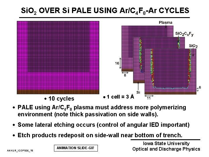
Si. O 2 OVER Si PALE USING Ar/C 4 F 8 -Ar CYCLES 1 cell = 3 Å · 10 cycles · PALE using Ar/C 4 F 8 plasma must address more polymerizing environment (note thick passivation on side walls). · Some lateral etching occurs (control of angular IED important) · Etch products redeposit on side-wall near bottom of trench. ANKUR_ICOPS 06_19 ANIMATION SLIDE-GIF Iowa State University Optical and Discharge Physics

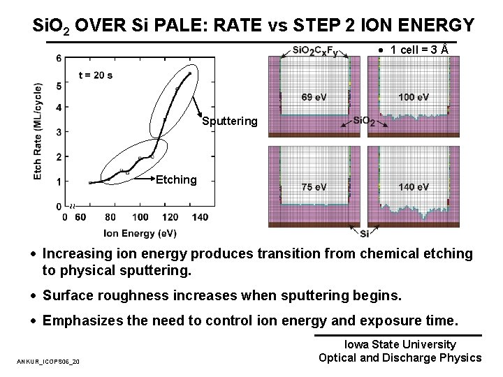
Si. O 2 OVER Si PALE: RATE vs STEP 2 ION ENERGY · 1 cell = 3 Å Sputtering Etching · Increasing ion energy produces transition from chemical etching to physical sputtering. · Surface roughness increases when sputtering begins. · Emphasizes the need to control ion energy and exposure time. ANKUR_ICOPS 06_20 Iowa State University Optical and Discharge Physics

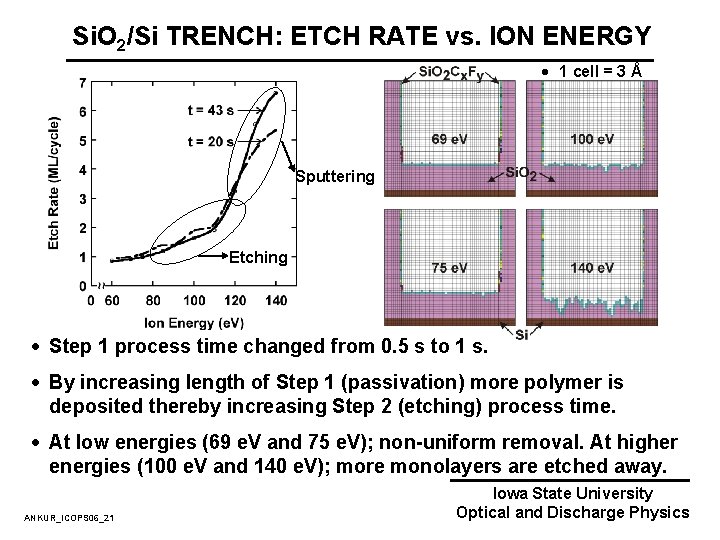
Si. O 2/Si TRENCH: ETCH RATE vs. ION ENERGY · 1 cell = 3 Å Sputtering Etching · Step 1 process time changed from 0. 5 s to 1 s. · By increasing length of Step 1 (passivation) more polymer is deposited thereby increasing Step 2 (etching) process time. · At low energies (69 e. V and 75 e. V); non-uniform removal. At higher energies (100 e. V and 140 e. V); more monolayers are etched away. ANKUR_ICOPS 06_21 Iowa State University Optical and Discharge Physics

CONCLUDING REMARKS · Atomic layer control of etch processes will be critical for 32 nm node devices. · PALE using conventional plasma equipment makes for an more economic processes. · Proof of principle calculations demonstrate Si-Fin. FET and Si/Si. O 2 deep trenches can be atomically etched in selfterminating Ar/Cl 2 mixtures. · Si. O 2/Si deep trenches can be atomically etched in selfterminating Ar/C 4 F 8 mixtures. · Control of angular distribution is critical to removing redeposited etch products on sidewalls. · Passivation step may induce unwanted etching: · Control length of exposure · Control ion energy ANKUR_ICOPS 06_22 Iowa State University Optical and Discharge Physics