2 Dry etching Outline Terminology Wet Etching Dry
 Dry etching")


 chemically assisted")


- Slides: 23
(2) Dry etching
Outline - Terminology - Wet Etching - Dry Etching - DRIE - Si / Si. O 2/ Si. N/ Metal Dry etching
Etch rate & Selectivity & Uniformity # Etch rate # Selectivity In same Plasma Condition EA = Etch Rate of Layer A EB = Etch Rate of Layer B SA/B : Selectivity of A to B # Uniformity Ei : Etch Rate at Several Points Emax : Maximum Etch Rate Emin : Minimum Etch Rate
Anisotropy
Selectivity
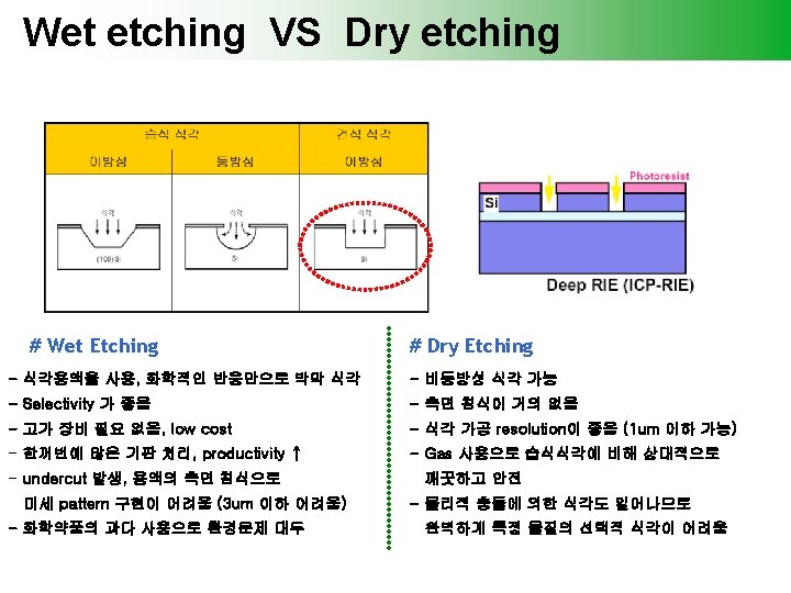
Etching terminology
Mechanism of wet etching
Mechanism of wet etching
Mechanism of wet etching
Mechanism of wet etching
Experimental conditions for Si wafer etching Pattern size 100㎛ 100 -1. 414 a=0 a= 100/1. 414=70. 72 Etch time 70/Etch rate of KOH per a hour =70/31=2. 26 hour Pattern size 400㎛ 400 -1. 414 a=0 a= 400/1. 414=282. 89 <100> Wafer Etch time 282. 89/Etch rate of KOH per a hour =282. 89/31=9. 13 hour
100 um patterns by Si wafer etching
Dry etching # Advantage - Uses small amounts of chemical - Isotropic or Anisotropic etch profile - Directional etching without using the crystal orientation of Si - High resolution and cleanliness - Less Undercutting # Disadvantage - Some gases are quite toxic - Need for specialized (expensive) equipment - Re-deposition of non-volatile compounds
Plasma enhanced chemical etching e- + Bulk Plasma e- + + + e- mask (mask erosion) + volatile product Sheath sidewall passivation + + reactive ion reactive species e- electron PR particle + λD ~ <1 mm e- Substrate e- e- Electrode e- e- x eplasma presheath Sheath 0 edge s
Various Plasma Etching Reactors Schematic configuration of several dry etching reactors; (a) chemically assisted ion beam etching (CAIBE) reactor, (b) reactive ion etching (RIE) chamber, (c) inductively coupled plasma (ICP) reactor, (d) electron cyclotron resonance (ECR) reactor.
Etching gas
Silicon etching – RIE system High rate Isotropic Oxide/Nitride/Si etch with good uniformity: Thermal oxide etch rate ~ 818Å/min ± 5% across 6” wafer, sel to AZ 6615 PR ~ 0. 5: 1 Single-crystal Si etch rate ~ 870 Å/min, sel to AZ 6615 ~ 0. 53: 1 Adjust pressure or power for uniformity. CF 4 35 sccm (or CHF 3) O 2 3 sccm 150 m. T 300 W (on 240 mm diameter electrode) -579 V 20 C, graphite cover plate Silicon etch using an Si. O 2 mask (150 m. T, 300 W) Silicon wet etching result Si (100) for convex cornor Henning Schröder, Ernst Obermeier, Anton Horn, and Gerhard K. M. Wachutka, J. Micros. Sys. , 2001, 10, 88
DRIE etch Principle # Bosch process - 1 st step : Etch (SF 6 gas) - 2 nd step : Deposit passivation layer (C 4 F 8 → CFx 계열로 분해) - 3 rd step : Wallside polymer etch << Bottom side polymer etch - 1 st step again : polymer and Silicon etch (SF 6 gas)
DRIE etch Principle # Passivation step and Etch step < Deposition step> - Coil power ↑ ▶ passivation rate ↑ - Coil power ↑ , Wafer Temperature ↑ ▶ passivation rate ↓ ∴ He back side cooling < Etch step > - Coil power, Gas flow ↑ ▶ SF 6 로부터 F • etchant species 많이 발생 ▶ etch rate ↑ - High pressure ▶ 높은 F • etchant species로 etch rate ↑
DRIE etch Principle # repeat the etch and passivation steps
Conclusion 1. Plasma etching is quite useful tool for fabricating ultra high precision machining with few micron scale or below. 2. Various materials (e. g. , Si. O 2, Si 3 N 4 and some metals) are etched with vertical profile and quick and simple procedure. 3. For nano-scale fabrication one’s needs will require an unique solution as an advanced plasma etching method.