Chap 10 Etching and implantation Wet etching Etching


 chemically assisted")


- Slides: 18
Chap 10. Etching and implantation
Wet etching
Etching gas
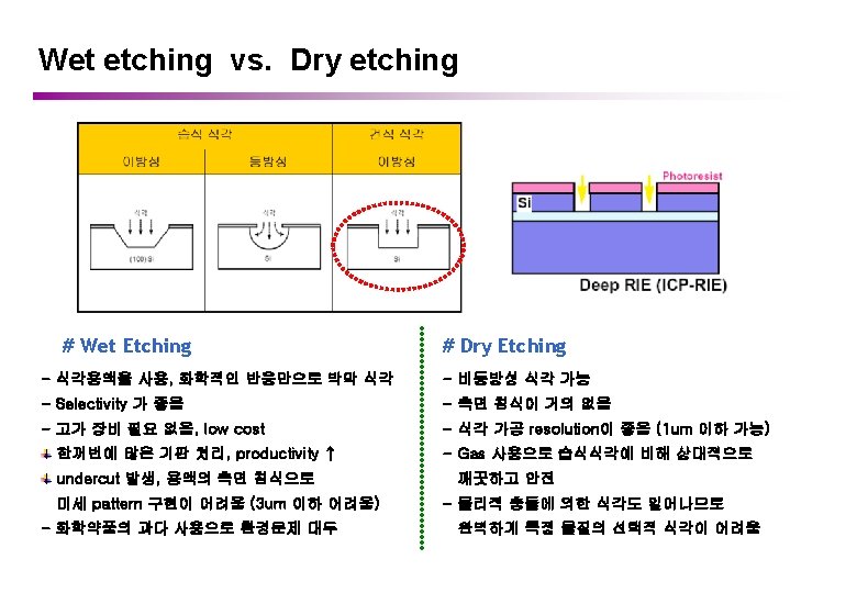
Wet etching
16. Etch
Plasma enhanced chemical etching e- + Bulk Plasma e- + + + e- mask (mask erosion) + volatile product Sheath sidewall passivation + + reactive ion reactive species e- electron PR particle + λD ~ <1 mm e- Substrate e- e- Electrode e- e- x eplasma presheath Sheath 0 edge s
16. Etch Dry etch Wet etch Etch bias selectivity
16. Etch Poor selectivity EPD RIE HDP etcher
16. Etch ECR ICP DPS MERIE EPD FC chemistry For oxide F > Cl > Br based For Silicon
Various Plasma Etching Reactors Schematic configuration of several dry etching reactors; (a) chemically assisted ion beam etching (CAIBE) reactor, (b) reactive ion etching (RIE) chamber, (c) inductively coupled plasma (ICP) reactor, (d) electron cyclotron resonance (ECR) reactor.
16. Etch Cl based For metal Ashing oxygen
17. Ion Implant doping Diffusion implanation
17. Ion Implant Predeposition Drive-in activation physical dose Concentration
17. Ion Implant
17. Ion Implant Thermal Anneal RTA Channeling
17. Ion Implant SOI SIMOX
SOI wafer DBW Direct Bonded Wafer Si Wafer SIMOX Separation by Implantation Oxygen Implantation Thermal Oxidation ; Si. O 2 Layer Bonding Si Wafer Heat Treatment Thinning of Si Layer Si Wafer Si. O 2 Layer