Etching and Cleaning remove contaminated layers Etching remove
- Slides: 17

Etching and Cleaning remove contaminated layers Etching remove defect layers, form pattern by selective material removal Basic steps: reaction + dissolution (or desorption Wet etching: using reactive chemical solution Dry etching: using reactive/energetic gas-phase species, including ions, atoms, radicals, plasma, laser…

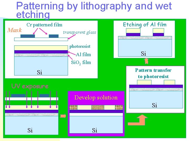
Patterning by lithography and wet etching Mask Etching of Al film Cr patterned film transparent glass photoresist Si Al film Si. O 2 film Pattern transfer to photoresist Si UV exposure Develop solution Si Si Si

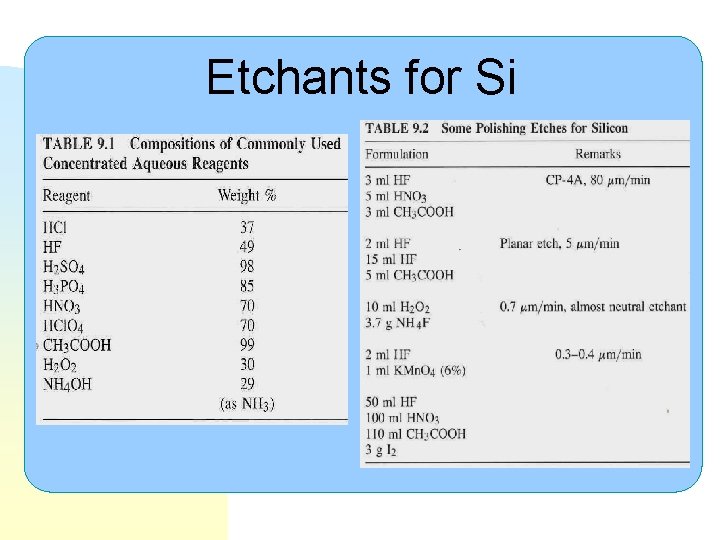
Etchants for Si

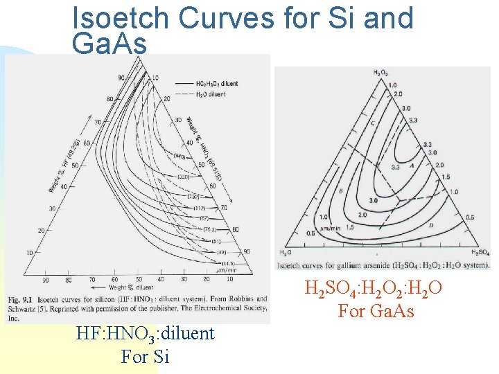
Isoetch Curves for Si and Ga. As H 2 SO 4: H 2 O 2: H 2 O For Ga. As HF: HNO 3: diluent For Si

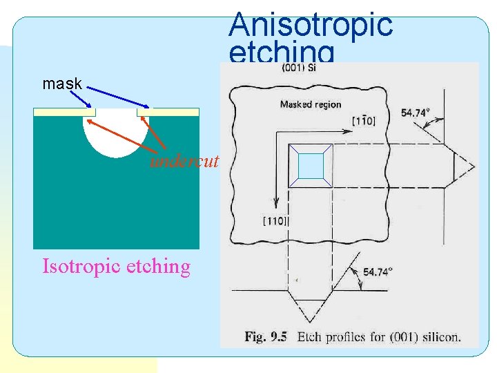
Anisotropic etching mask undercut Isotropic etching

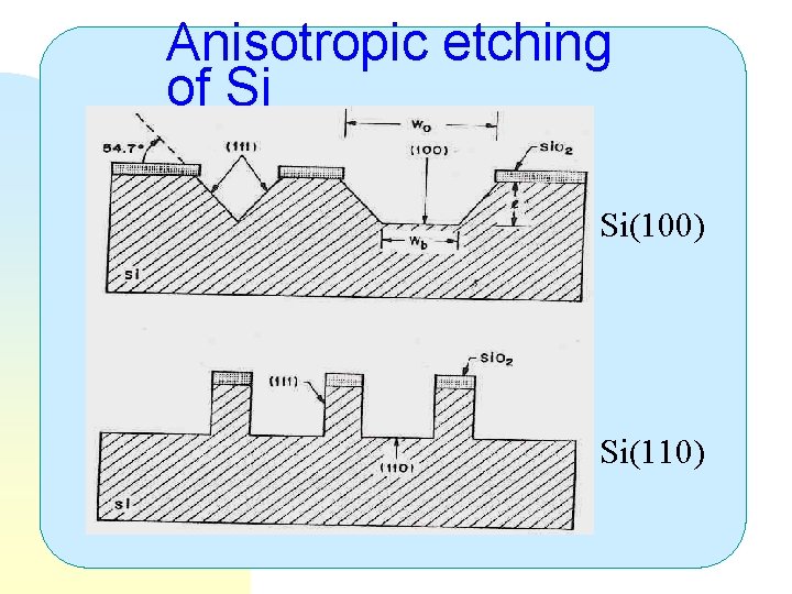
Anisotropic etching of Si Si(100) Si(110)

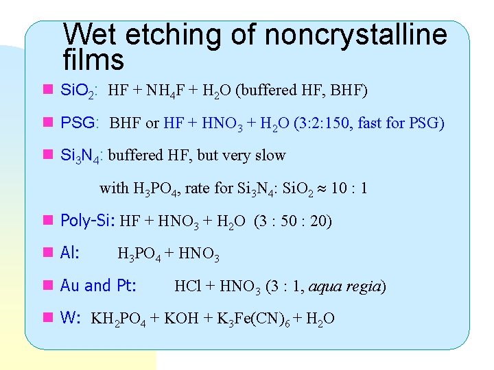
Wet etching of noncrystalline films n Si. O 2: HF + NH 4 F + H 2 O (buffered HF, BHF) n PSG: BHF or HF + HNO 3 + H 2 O (3: 2: 150, fast for PSG) n Si 3 N 4: buffered HF, but very slow with H 3 PO 4, rate for Si 3 N 4: Si. O 2 10 : 1 n Poly-Si: HF + HNO 3 + H 2 O (3 : 50 : 20) n Al: H 3 PO 4 + HNO 3 n Au and Pt: HCl + HNO 3 (3 : 1, aqua regia) n W: KH 2 PO 4 + KOH + K 3 Fe(CN)6 + H 2 O

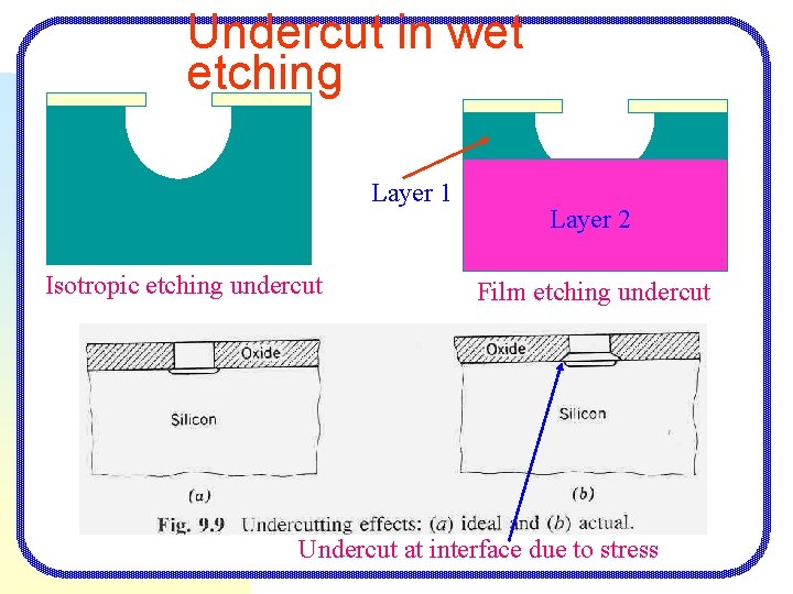
Undercut in wet etching Layer 1 Isotropic etching undercut Layer 2 Film etching undercut Undercut at interface due to stress

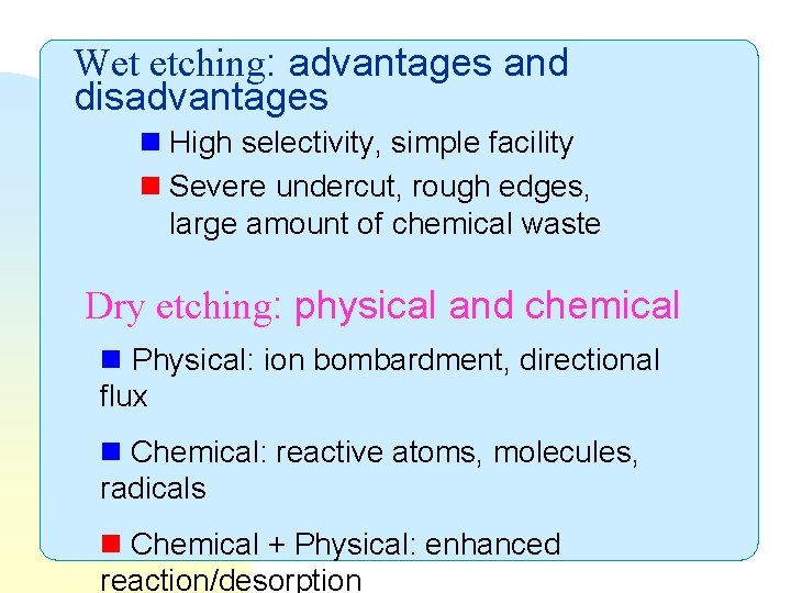
Wet etching: advantages and disadvantages n High selectivity, simple facility n Severe undercut, rough edges, large amount of chemical waste Dry etching: physical and chemical n Physical: ion bombardment, directional flux n Chemical: reactive atoms, molecules, radicals n Chemical + Physical: enhanced reaction/desorption

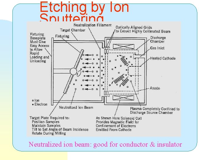
Etching by Ion Sputtering Neutralized ion beam: good for conductor & insulator

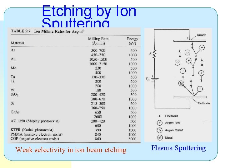
Etching by Ion Sputtering Weak selectivity in ion beam etching Plasma Sputtering

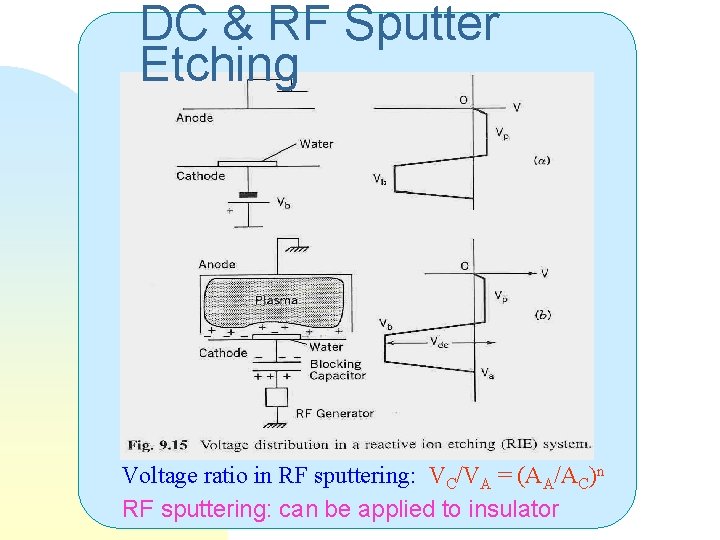
DC & RF Sputter Etching Voltage ratio in RF sputtering: VC/VA = (AA/AC)n RF sputtering: can be applied to insulator

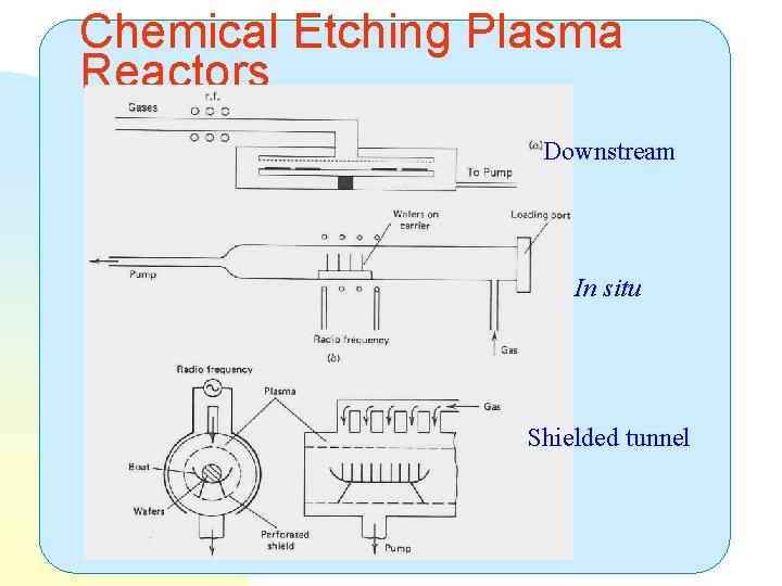
Chemical Etching Plasma Reactors Downstream In situ Shielded tunnel

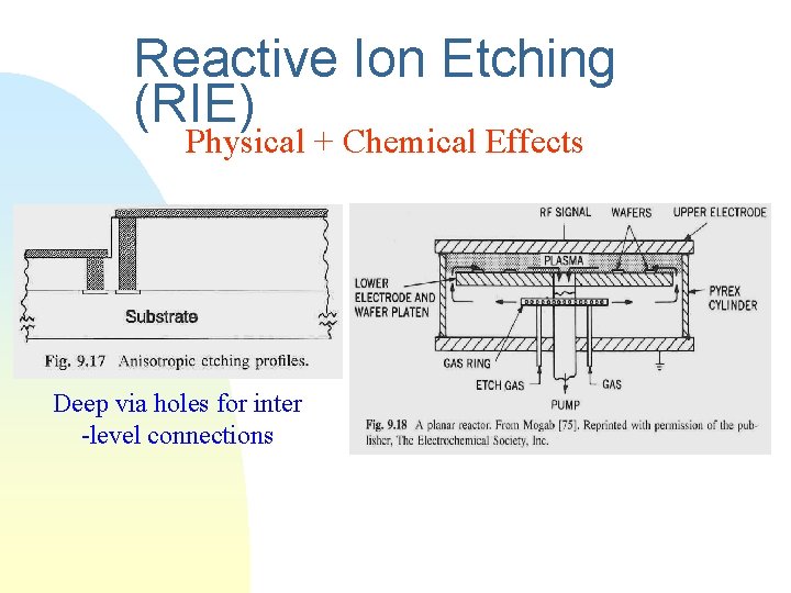
Reactive Ion Etching (RIE) Physical + Chemical Effects Deep via holes for inter -level connections

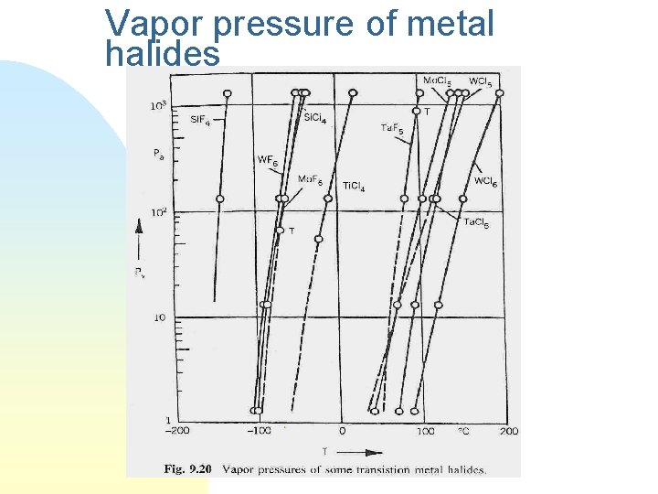
Vapor pressure of metal halides

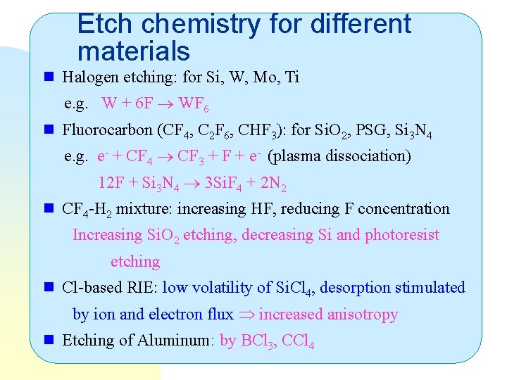
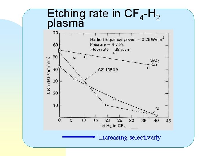
Etch chemistry for different materials n Halogen etching: for Si, W, Mo, Ti e. g. W + 6 F WF 6 n Fluorocarbon (CF 4, C 2 F 6, CHF 3): for Si. O 2, PSG, Si 3 N 4 e. g. e- + CF 4 CF 3 + F + e- (plasma dissociation) 12 F + Si 3 N 4 3 Si. F 4 + 2 N 2 n CF 4 -H 2 mixture: increasing HF, reducing F concentration Increasing Si. O 2 etching, decreasing Si and photoresist etching n Cl-based RIE: low volatility of Si. Cl 4, desorption stimulated by ion and electron flux increased anisotropy n Etching of Aluminum: by BCl 3, CCl 4

Etching rate in CF 4 -H 2 plasma Increasing selectiveity