WET ETCHING OF RUTHENIUM EFFECT OF THERMAL ANNEALING

![RUTHENIUM: METAL OF CHOICE FOR BEOL INTERCONNECT R [W/mm] § Ru: Interconnect alternative to RUTHENIUM: METAL OF CHOICE FOR BEOL INTERCONNECT R [W/mm] § Ru: Interconnect alternative to](https://slidetodoc.com/presentation_image_h/a2f10e7af78281bdf3da92ef2871d9b7/image-4.jpg)




- Slides: 21

WET ETCHING OF RUTHENIUM: EFFECT OF THERMAL ANNEALING Q. T. LE, E. KESTERS, H. PHILIPSEN, AND F. HOLSTEYNS IMEC, LEUVEN, BELGIUM Email address: Quoc. Toan. Le@imec. be SPCC 2019, Portland, April 1 -3 rd, PUBLIC

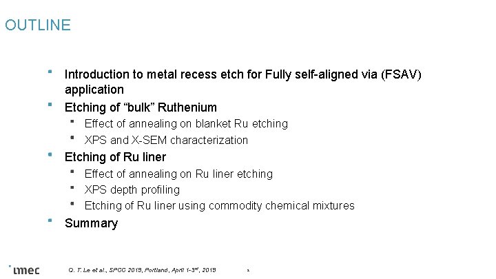
OUTLINE Introduction to metal recess etch for Fully self-aligned via (FSAV) application Etching of “bulk” Ruthenium Effect of annealing on blanket Ru etching XPS and X-SEM characterization Etching of Ru liner Effect of annealing on Ru liner etching XPS depth profiling Etching of Ru liner using commodity chemical mixtures Summary Q. T. Le et al. , SPCC 2019, Portland, April 1 -3 rd, 2019 2

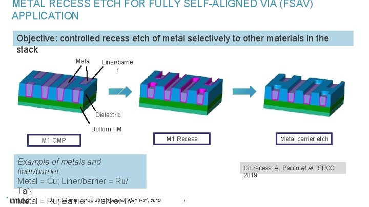
METAL RECESS ETCH FOR FULLY SELF-ALIGNED VIA (FSAV) APPLICATION Objective: controlled recess etch of metal selectively to other materials in the stack Metal Liner/barrie r Dielectric Bottom HM M 1 Recess M 1 CMP Example of metals and liner/barrier: Metal = Cu; Liner/barrier = Ru/ Ta. N Q. T. Le et al. , SPCC 2019, Portland, April 1 -3 Metal = Ru; Barrier = Ta. N or Ti. N Metal barrier etch Co recess: A. Pacco et al. , SPCC 2019 rd, 2019 3
![RUTHENIUM METAL OF CHOICE FOR BEOL INTERCONNECT R Wmm Ru Interconnect alternative to RUTHENIUM: METAL OF CHOICE FOR BEOL INTERCONNECT R [W/mm] § Ru: Interconnect alternative to](https://slidetodoc.com/presentation_image_h/a2f10e7af78281bdf3da92ef2871d9b7/image-4.jpg)
RUTHENIUM: METAL OF CHOICE FOR BEOL INTERCONNECT R [W/mm] § Ru: Interconnect alternative to Cu § Candidate as barrier-less metallization for interconnect § Ru vs. Cu: Ru outperforms Cu both for line and via resistance below 12 nm CD § Ru has been used as a liner layer Line CD [nm] Q. T. Le et al. , SPCC 2019, Portland, April 1 -3 rd, 2019 4 o M. van der Veen et al. , IITC 2018. o H. Philipsen et al. , Electrochimica Acta (2018), https: //doi. org/10. 1016/j. electacta. 2018. 04. 093 o H. Philipsen et al. , Electrochimica Acta (2019), https: //doi. org/10. 1016/j. electacta. 2019. 03. 065

ETCHING OF “BULK” RUTHENIUM

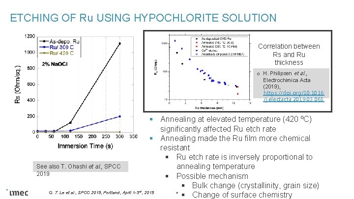
ETCHING OF Ru USING HYPOCHLORITE SOLUTION Correlation between Rs and Ru thickness o H. Philipsen et al. , Electrochimica Acta (2019), https: //doi. org/10. 1016 /j. electacta. 2019. 03. 065 See also T. Ohashi et al. , SPCC 2019 § Annealing at elevated temperature (420 ºC) significantly affected Ru etch rate § Annealing made the Ru film more chemical resistant § Ru etch rate is inversely proportional to annealing temperature § Possible mechanism § Bulk change (crystallinity, grain size) , 2019 § Change of surface chemistry Q. T. Le et al. , SPCC 2019, Portland, April 1 -3 rd 6

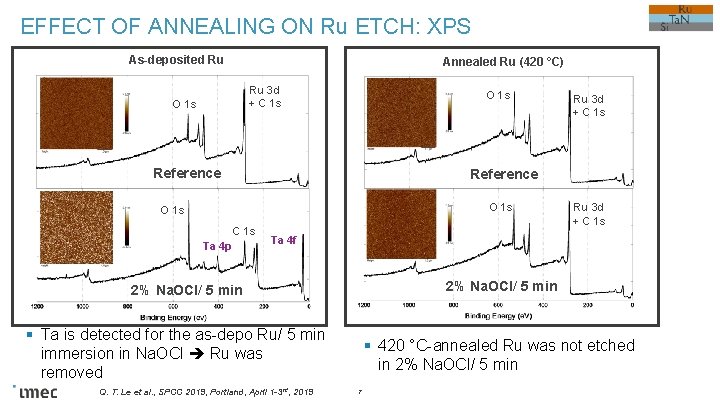
EFFECT OF ANNEALING ON Ru ETCH: XPS As-deposited Ru Annealed Ru (420 °C) Ru 3 d + C 1 s O 1 s Reference Ru 3 d + C 1 s Reference O 1 s C 1 s Ta 4 p Ru 3 d + C 1 s Ta 4 f 2% Na. OCl/ 5 min § Ta is detected for the as-depo Ru/ 5 min immersion in Na. OCl Ru was removed Q. T. Le et al. , SPCC 2019, Portland, April 1 -3 rd, 2019 § 420 °C-annealed Ru was not etched in 2% Na. OCl/ 5 min 7

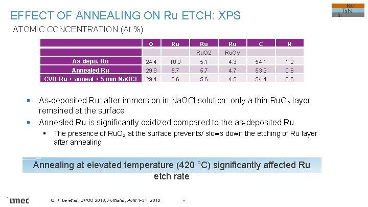
EFFECT OF ANNEALING ON Ru ETCH: XPS ATOMIC CONCENTRATION (At. %) As-depo. Ru Annealed Ru CVD-Ru + anneal + 5 min Na. OCl § § O Ru Ru Ru C N Ru. O 2 Ru. Oy 24. 4 10. 9 5. 1 4. 3 54. 1 1. 2 29. 9 5. 7 4. 7 53. 3 0. 6 29. 4 5. 6 4. 5 54. 4 0. 6 As-deposited Ru: after immersion in Na. OCl solution: only a thin Ru. O 2 layer remained at the surface Annealed Ru is significantly oxidized compared to the as-deposited Ru § The presence of Ru. O 2 at the surface prevents/ slows down the etching of Ru layer after annealing Annealing at elevated temperature (420 °C) significantly affected Ru etch rate Q. T. Le et al. , SPCC 2019, Portland, April 1 -3 rd, 2019 8

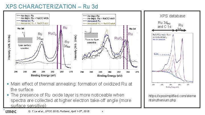
XPS CHARACTERIZATION – Ru 3 d XPS database Ru 3 d 3/2 and C 1 s Ru Ru 3 d 3/2 Ru. O 2 Ru 3 d 5/2 Ru Ru. O 2 Ru 3 d 5/2 § Main effect of thermal annealing: formation of oxidized Ru at the surface § The presence of Ru oxide layer is more noticeable when spectra are collected at higher electron take-off angle (more surface sensitive) Q. T. Le et al. , SPCC 2019, Portland, April 1 -3 rd, 2019 9 https: //xpssimplified. com/eleme nts/ruthenium. php

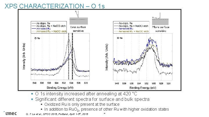
XPS CHARACTERIZATION – O 1 s § O 1 s intensity increased after annealing at 420 °C § Significant different spectra for surface and bulk spectra § Oxidized Ru is only present at the surface § In addition to Ru. O 2, presence of other Ru with higher oxidation states Q. T. Le et al. , SPCC 2019, Portland, April 1 -3 rd, 2019 10

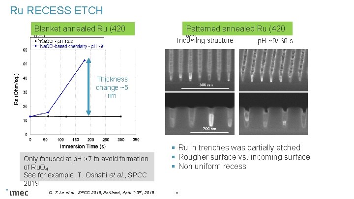
Ru RECESS ETCH Blanket annealed Ru (420 ºC) Patterned annealed Ru (420 ºC) Incoming structure p. H ~9/ 60 s Thickness change ~5 nm Only focused at p. H >7 to avoid formation of Ru. O 4 See for example, T. Oshahi et al. , SPCC 2019 Q. T. Le et al. , SPCC 2019, Portland, April 1 -3 rd, 2019 § Ru in trenches was partially etched § Rougher surface vs. incoming surface § Non uniform recess 11

ETCHING OF RUTHENIUM LINER

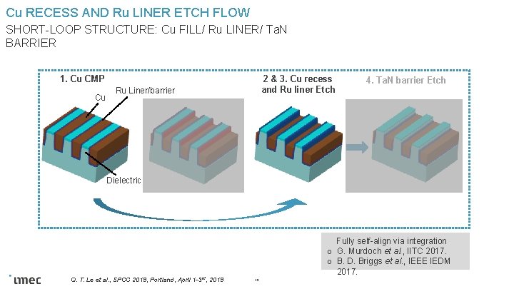
Cu RECESS AND Ru LINER ETCH FLOW SHORT-LOOP STRUCTURE: Cu FILL/ Ru LINER/ Ta. N BARRIER 1. Cu CMP Cu 2 & 3. Cu recess and Ru liner Etch Ru Liner/barrier 4. Ta. N barrier Etch Dielectric Q. T. Le et al. , SPCC 2019, Portland, April 1 -3 rd, 2019 Fully self-align via integration o G. Murdoch et al. , IITC 2017. o B. D. Briggs et al. , IEEE IEDM 2017. 13

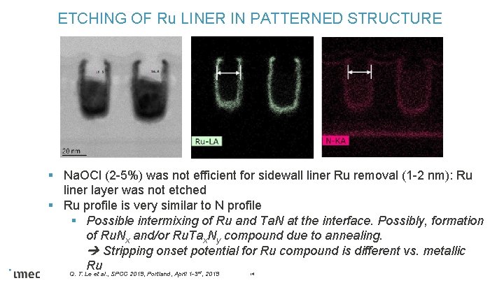
ETCHING OF Ru LINER IN PATTERNED STRUCTURE § Na. OCl (2 -5%) was not efficient for sidewall liner Ru removal (1 -2 nm): Ru liner layer was not etched § Ru profile is very similar to N profile § Possible intermixing of Ru and Ta. N at the interface. Possibly, formation of Ru. Nx and/or Ru. Tax. Ny compound due to annealing. Stripping onset potential for Ru compound is different vs. metallic Ru Q. T. Le et al. , SPCC 2019, Portland, April 1 -3 , 2019 rd 14

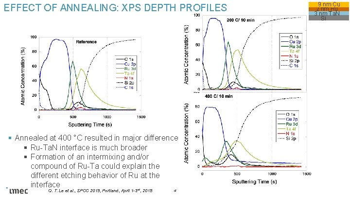
EFFECT OF ANNEALING: XPS DEPTH PROFILES § Annealed at 400 °C resulted in major difference § Ru-Ta. N interface is much broader § Formation of an intermixing and/or compound of Ru-Ta could explain the different etching behavior of Ru at the interface Q. T. Le et al. , SPCC 2019, Portland, April 1 -3 rd, 2019 15 9 nm Cu 2 nm Ru 3 nm Ta. N Si

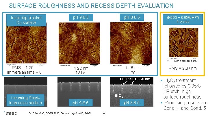
SURFACE ROUGHNESS AND RECESS DEPTH EVALUATION Incoming blanket Cu surface p. H 8 -8. 5 p. H 9 -9. 5 (H 2 O 2 + 0. 05% HF*) 4 cycles * HF with saturated DO RMS = 1. 20 Immersion time = 0 nm s Incoming Shortloop cross section 1. 15 nm 120 s 1. 22 nm 120 s Cu line CD ~20 nm Si. O 2 p. H 8 -8. 5 p. H 9 -9. 5 Q. T. Le et al. , SPCC 2019, Portland, April 1 -3 rd, 2019 16 RMS = 2. 37 nm § H 2 O 2 treatment followed by 0. 05% HF etch: high surface roughness § Promising results for Cond. 4 and Cond. 5

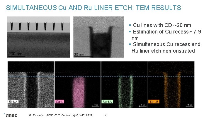
SIMULTANEOUS Cu AND Ru LINER ETCH: TEM RESULTS § Cu lines with CD ~20 nm § Estimation of Cu recess ~7 -9 nm § Simultaneous Cu recess and Ru liner etch demonstrated Q. T. Le et al. , SPCC 2019, Portland, April 1 -3 rd, 2019 17

SUMMARY

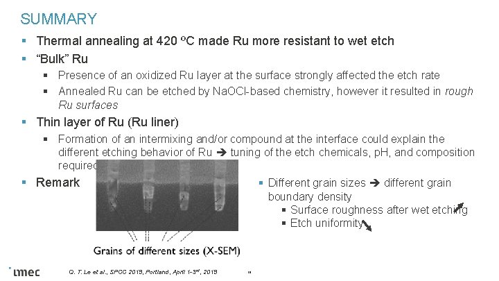
SUMMARY § Thermal annealing at 420 ºC made Ru more resistant to wet etch § “Bulk” Ru § Presence of an oxidized Ru layer at the surface strongly affected the etch rate § Annealed Ru can be etched by Na. OCl-based chemistry, however it resulted in rough Ru surfaces § Thin layer of Ru (Ru liner) § Formation of an intermixing and/or compound at the interface could explain the different etching behavior of Ru tuning of the etch chemicals, p. H, and composition required § Remark Q. T. Le et al. , SPCC 2019, Portland, April 1 -3 rd, 2019 § Different grain sizes different grain boundary density § Surface roughness after wet etching § Etch uniformity 19

ACKNOWLEDGEMENTS Integration: Chris Wilson, Gayle Murdoch, Guillaume Boccardi Surface and Interface Processing and CMP: Antoine Pacco, Nancy Heylen, Katia Devriendt Characterization (XPS, AFM, TEM, RBS): Thierry Conard, Ilse Hoflijk, Inge Vaesen, Danielle Vanhaeren, Stefanie Sergeant, Eric Vancoille, Kris Paulussen, Laura Nelissen, Hugo Bender, Johan Meersschaut, Johan Desmet Q. T. Le et al. , SPCC 2019, Portland, April 1 -3 rd, 2019 20

PUBLIC