Nios II Processor Architecture and Programming CEG 4131
![Stratix EP 1 S 10 [2] 3 Stratix EP 1 S 10 [2] 3](https://slidetodoc.com/presentation_image_h/c9c8c284b76cb43d05f2af5bf5d0be05/image-3.jpg)
![Tri. Matrix™ Memory [1] M 512 Blocks n n Small FIFOs Shift Register Rake Tri. Matrix™ Memory [1] M 512 Blocks n n Small FIFOs Shift Register Rake](https://slidetodoc.com/presentation_image_h/c9c8c284b76cb43d05f2af5bf5d0be05/image-6.jpg)
![Memory Bandwidth Summary Stratix Device Family [1] Device Total RAM Bits M-RAM Blocks EP Memory Bandwidth Summary Stratix Device Family [1] Device Total RAM Bits M-RAM Blocks EP](https://slidetodoc.com/presentation_image_h/c9c8c284b76cb43d05f2af5bf5d0be05/image-7.jpg)
![Logic Element (LE) [2] LUT Chain Input Register Chain Input addnsub Register Control Signals Logic Element (LE) [2] LUT Chain Input Register Chain Input addnsub Register Control Signals](https://slidetodoc.com/presentation_image_h/c9c8c284b76cb43d05f2af5bf5d0be05/image-9.jpg)
![Logic Array Blocks (LAB) [2] Control Signals • 10 LEs • Local Interconnect • Logic Array Blocks (LAB) [2] Control Signals • 10 LEs • Local Interconnect •](https://slidetodoc.com/presentation_image_h/c9c8c284b76cb43d05f2af5bf5d0be05/image-10.jpg)
![NIOS II Overview [3] • Soft IP Core – A soft-core processor is a NIOS II Overview [3] • Soft IP Core – A soft-core processor is a](https://slidetodoc.com/presentation_image_h/c9c8c284b76cb43d05f2af5bf5d0be05/image-13.jpg)
![NIOS II Processor Core [3] 15 NIOS II Processor Core [3] 15](https://slidetodoc.com/presentation_image_h/c9c8c284b76cb43d05f2af5bf5d0be05/image-15.jpg)
![Hardware Abstraction Layer (HAL) [4] • Isolates the application software from hardware modifications. • Hardware Abstraction Layer (HAL) [4] • Isolates the application software from hardware modifications. •](https://slidetodoc.com/presentation_image_h/c9c8c284b76cb43d05f2af5bf5d0be05/image-26.jpg)
![Layers of HAL API [4] • HAL library generatioin: 1. SOPC Builder generates a Layers of HAL API [4] • HAL library generatioin: 1. SOPC Builder generates a](https://slidetodoc.com/presentation_image_h/c9c8c284b76cb43d05f2af5bf5d0be05/image-27.jpg)
![Programming NIOS II Processor [4] • Programming UART – Standard Input, Standard Output routines Programming NIOS II Processor [4] • Programming UART – Standard Input, Standard Output routines](https://slidetodoc.com/presentation_image_h/c9c8c284b76cb43d05f2af5bf5d0be05/image-28.jpg)
- Slides: 29

Nios II Processor Architecture and Programming CEG 4131 Computer Architecture III Miodrag Bolic 1

Presentation Outline • Basic description of Stratix Altera Devices • NIOS II processor architecture – Review pipelining techniques – Review memory access techniques • How to design a system using NIOS II processor 2
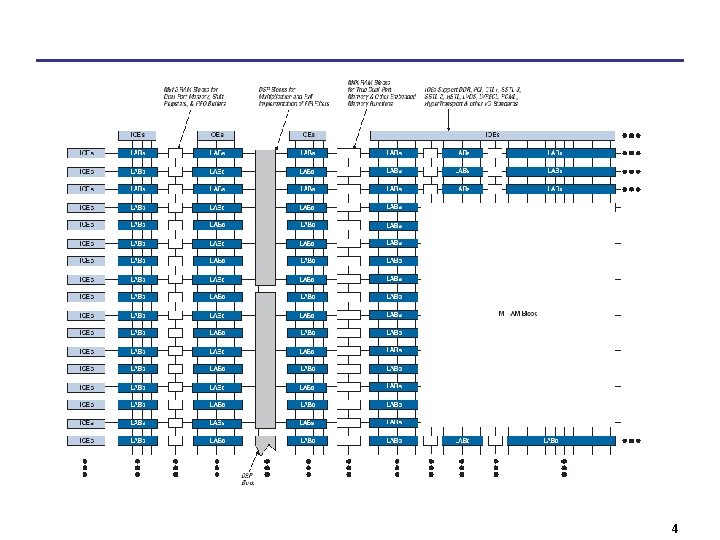
![Stratix EP 1 S 10 2 3 Stratix EP 1 S 10 [2] 3](https://slidetodoc.com/presentation_image_h/c9c8c284b76cb43d05f2af5bf5d0be05/image-3.jpg)
Stratix EP 1 S 10 [2] 3

4

5
![Tri Matrix Memory 1 M 512 Blocks n n Small FIFOs Shift Register Rake Tri. Matrix™ Memory [1] M 512 Blocks n n Small FIFOs Shift Register Rake](https://slidetodoc.com/presentation_image_h/c9c8c284b76cb43d05f2af5bf5d0be05/image-6.jpg)
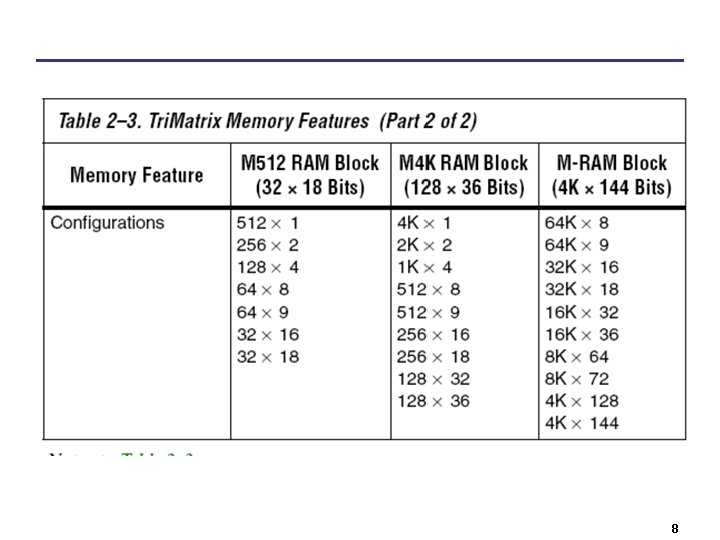
Tri. Matrix™ Memory [1] M 512 Blocks n n Small FIFOs Shift Register Rake Receiver Correlator FIR Filter Delay Line M 4 K Blocks n n Header / Cell Storage n Channelized Functions n n ATM cell–packet processing n Nios Program Memory n Dedicated External Memory Interface M-RAM Packet / Data Storage Nios Program Memory System Cache Video Frame Buffers Echo Canceller Data Storage n n n Look-Up Schemes Packet & Cell Buffering Cache More Bits For Larger Memory Buffering 512 bits per block + parity 4 Kbits per block + parity 512 Kbits per block + parity More Data Ports for Greater Memory Bandwidth 6
![Memory Bandwidth Summary Stratix Device Family 1 Device Total RAM Bits MRAM Blocks EP Memory Bandwidth Summary Stratix Device Family [1] Device Total RAM Bits M-RAM Blocks EP](https://slidetodoc.com/presentation_image_h/c9c8c284b76cb43d05f2af5bf5d0be05/image-7.jpg)
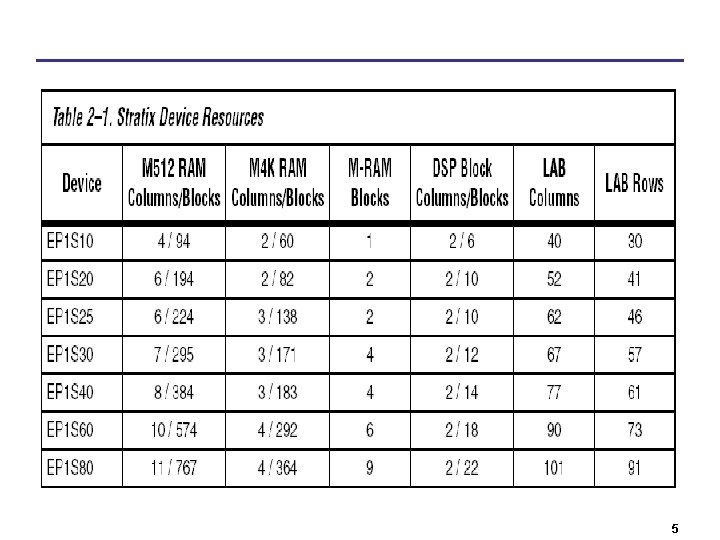
Memory Bandwidth Summary Stratix Device Family [1] Device Total RAM Bits M-RAM Blocks EP 1 S 10 920, 448 1 EP 1 S 20 1, 669, 248 EP 1 S 25 M 4 K Blocks M 512 Blocks Maximum Bandwidth (Mbps) 60 94 1, 245, 024 2 82 194 2, 096, 928 1, 944, 576 2 138 224 2, 894, 400 EP 1 S 30 3, 317, 184 4 171 295 3, 750, 192 EP 1 S 40 3, 423, 744 4 183 384 4, 384, 800 EP 1 S 60 5, 215, 104 6 292 574 6, 762, 528 EP 1 S 80 7, 427, 520 9 364 767 8, 784, 720 7

8
![Logic Element LE 2 LUT Chain Input Register Chain Input addnsub Register Control Signals Logic Element (LE) [2] LUT Chain Input Register Chain Input addnsub Register Control Signals](https://slidetodoc.com/presentation_image_h/c9c8c284b76cb43d05f2af5bf5d0be05/image-9.jpg)
Logic Element (LE) [2] LUT Chain Input Register Chain Input addnsub Register Control Signals cin data 1 data 2 data 3 (2) Sync Load & Clear Logic 4 -Input LUT D DATA data 4 Row, Column & Direct. Link Routing Local Routing Register Feedback LUT Chain Output Register Chain Output Note: 1) 2) Functional Diagram Only. Please See Datasheet for more Details. Addnsum & data 1 connected via XOR logic 9
![Logic Array Blocks LAB 2 Control Signals 10 LEs Local Interconnect Logic Array Blocks (LAB) [2] Control Signals • 10 LEs • Local Interconnect •](https://slidetodoc.com/presentation_image_h/c9c8c284b76cb43d05f2af5bf5d0be05/image-10.jpg)
Logic Array Blocks (LAB) [2] Control Signals • 10 LEs • Local Interconnect • LAB-Wide Control Signals 4 Local Interconnect 4 4 4 4 4 LE 1 LE 2 LE 3 LE 4 LE 5 LE 6 LE 7 LE 8 LE 9 LE 10 10

Presentation Outline • Basic description of Stratix Altera Devices • NIOS II processor architecture – Review pipelining techniques – Review memory access techniques • How to design a system using NIOS II processor 11

12
![NIOS II Overview 3 Soft IP Core A softcore processor is a NIOS II Overview [3] • Soft IP Core – A soft-core processor is a](https://slidetodoc.com/presentation_image_h/c9c8c284b76cb43d05f2af5bf5d0be05/image-13.jpg)
NIOS II Overview [3] • Soft IP Core – A soft-core processor is a microprocessor fully described in software, usually in an HDL, which can be synthesized in programmable hardware, such as FPGAs. • • • Reduced Instruction Set Computer (RISC) No pipeline, 5 or 6 stages pipeline configurations Full 32 -bit instruction set, data path, and address space 32 general-purpose registers 32 external interrupt sources Access to a variety of on-chip peripherals, and interfaces to off-chip memories and peripherals • Software development environment based on the GNU C/C++ tool chain and Eclipse IDE 13

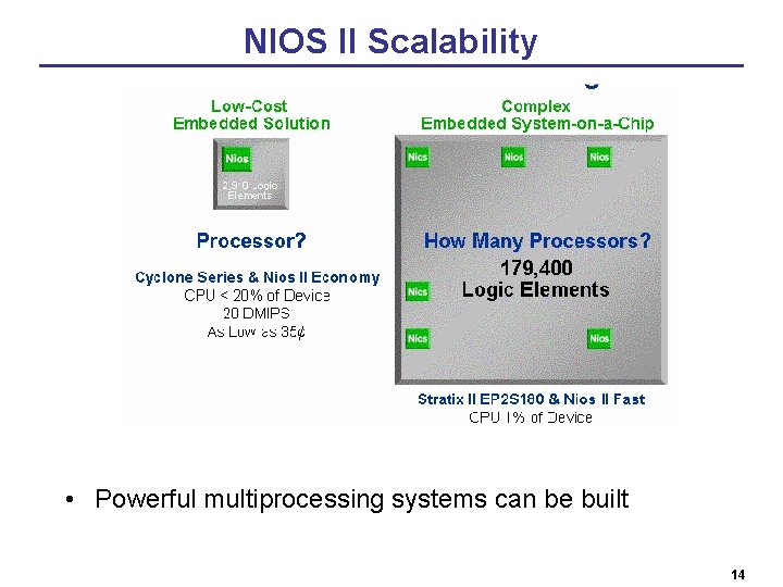
NIOS II Scalability • Powerful multiprocessing systems can be built 14
![NIOS II Processor Core 3 15 NIOS II Processor Core [3] 15](https://slidetodoc.com/presentation_image_h/c9c8c284b76cb43d05f2af5bf5d0be05/image-15.jpg)
NIOS II Processor Core [3] 15

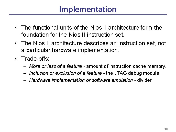
Implementation • The functional units of the Nios II architecture form the foundation for the Nios II instruction set. • The Nios II architecture describes an instruction set, not a particular hardware implementation. • Trade-offs: – More or less of a feature - amount of instruction cache memory. – Inclusion or exclusion of a feature - the JTAG debug module. – Hardware implementation or software emulation - divider 16

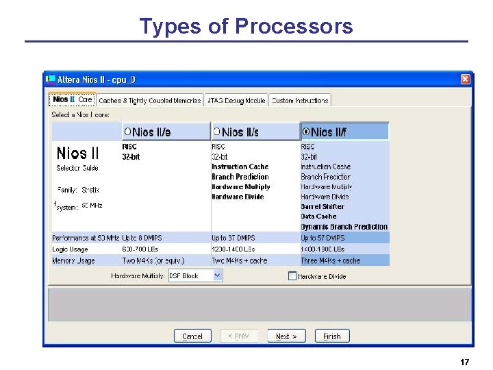
Types of Processors 17

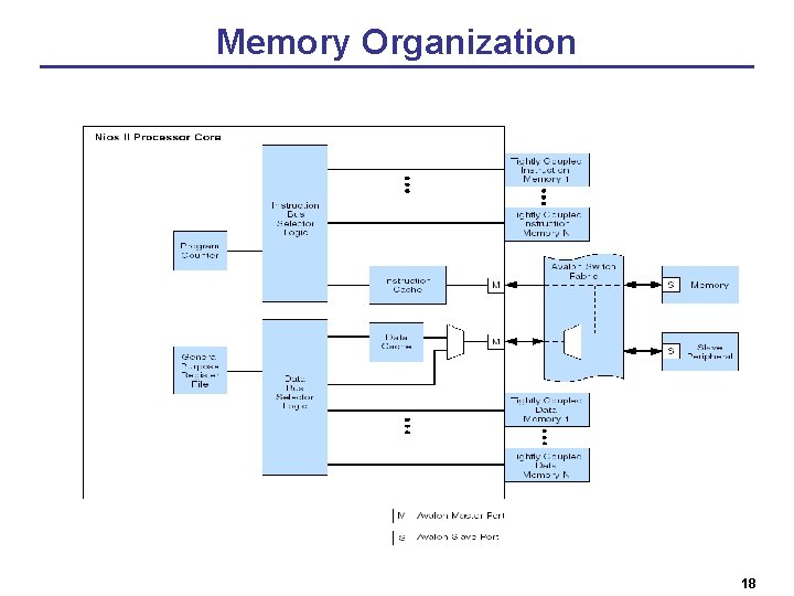
Memory Organization 18

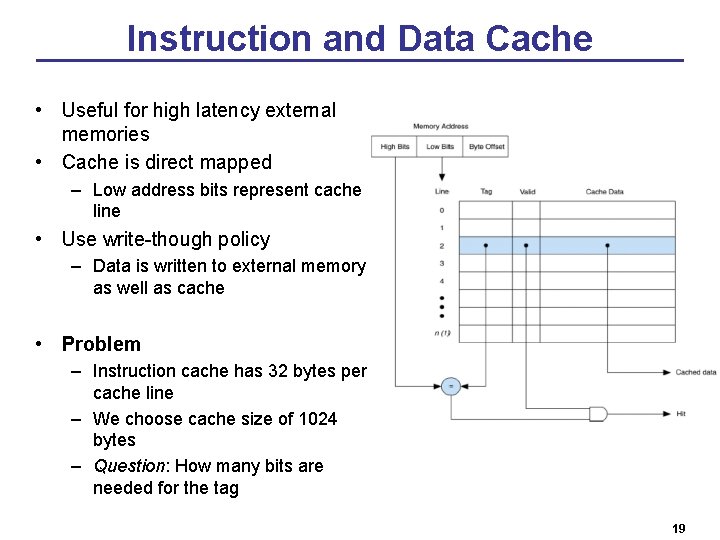
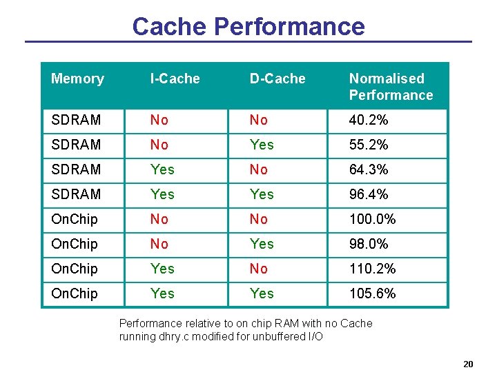
Instruction and Data Cache • Useful for high latency external memories • Cache is direct mapped – Low address bits represent cache line • Use write-though policy – Data is written to external memory as well as cache • Problem – Instruction cache has 32 bytes per cache line – We choose cache size of 1024 bytes – Question: How many bits are needed for the tag 19

Cache Performance Memory I-Cache D-Cache Normalised Performance SDRAM No No 40. 2% SDRAM No Yes 55. 2% SDRAM Yes No 64. 3% SDRAM Yes 96. 4% On. Chip No No 100. 0% On. Chip No Yes 98. 0% On. Chip Yes No 110. 2% On. Chip Yes 105. 6% Performance relative to on chip RAM with no Cache running dhry. c modified for unbuffered I/O 20

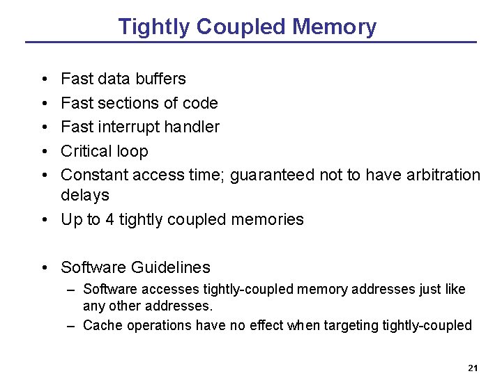
Tightly Coupled Memory • • • Fast data buffers Fast sections of code Fast interrupt handler Critical loop Constant access time; guaranteed not to have arbitration delays • Up to 4 tightly coupled memories • Software Guidelines – Software accesses tightly-coupled memory addresses just like any other addresses. – Cache operations have no effect when targeting tightly-coupled 21

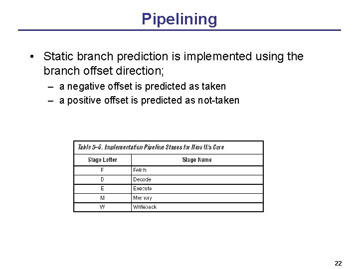
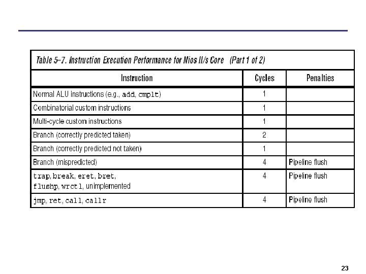
Pipelining • Static branch prediction is implemented using the branch offset direction; – a negative offset is predicted as taken – a positive offset is predicted as not-taken 22

23

Presentation Outline • Basic description of Stratix Altera Devices • NIOS II processor architecture – Review pipelining techniques – Review memory access techniques • How to design a system using NIOS II processor 24

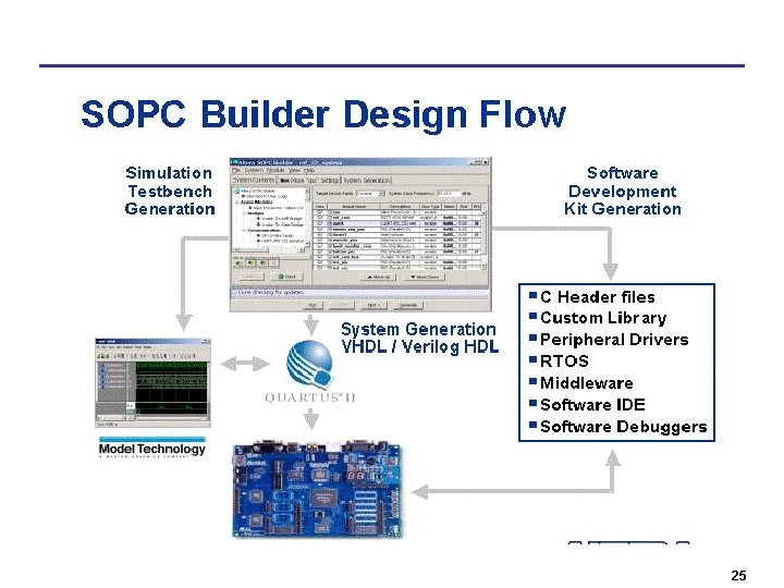
25
![Hardware Abstraction Layer HAL 4 Isolates the application software from hardware modifications Hardware Abstraction Layer (HAL) [4] • Isolates the application software from hardware modifications. •](https://slidetodoc.com/presentation_image_h/c9c8c284b76cb43d05f2af5bf5d0be05/image-26.jpg)
Hardware Abstraction Layer (HAL) [4] • Isolates the application software from hardware modifications. • Applications are device-independent because they abstract information from such systems as: – Character mode devices: UART core, JTAG UART core, LCD display controller – Flash memory devices – Timer devices – DMA controller core – Ethernet MAC/PHY Controller • HAL application program interface (API) is integrated with the ANSI C standard library. 26
![Layers of HAL API 4 HAL library generatioin 1 SOPC Builder generates a Layers of HAL API [4] • HAL library generatioin: 1. SOPC Builder generates a](https://slidetodoc.com/presentation_image_h/c9c8c284b76cb43d05f2af5bf5d0be05/image-27.jpg)
Layers of HAL API [4] • HAL library generatioin: 1. SOPC Builder generates a hardware system 2. Nios II IDE generates a custom HAL system library to match the hardware configuration • • Changes in the hardware configuration automatically propagate to the HAL device driver configuration NIOS II is programmed in C 27
![Programming NIOS II Processor 4 Programming UART Standard Input Standard Output routines Programming NIOS II Processor [4] • Programming UART – Standard Input, Standard Output routines](https://slidetodoc.com/presentation_image_h/c9c8c284b76cb43d05f2af5bf5d0be05/image-28.jpg)
Programming NIOS II Processor [4] • Programming UART – Standard Input, Standard Output routines in C -------------------------#include <stdio. h> #include <string. h> int main (void) { char* msg = “hello world”; FILE* fp; fp = fopen (“/dev/uart 1”, “w”); if (fp) { fprintf(fp, “%s”, msg); fclose (fp); } return 0; } -------------------------28

References 1. Altera Corp. , Stratix & Stratix II Module 3: Using Tri. Matrix Memories, 2004 2. Altera Corp. , Stratix Module 2: Logic Structure & Multi. Track Interconnect, 2004. 3. Altera Corp. , Nios II Processor Reference Handbook, 2005. 4. Altera Corp. , Nios II Software Developer's Handbook, 2005. 29