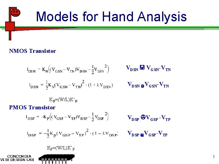
Models for Hand Analysis NMOS Transistor VDSN VGSNVTN
- Slides: 25

Models for Hand Analysis NMOS Transistor VDSN VGSN-VTN VDSN VGSN-VTN KN=(W/L)K’N PMOS Transistor VDSP VGSP -VTP VDSP VGSP-VTP KP=(W/L)K’P 1

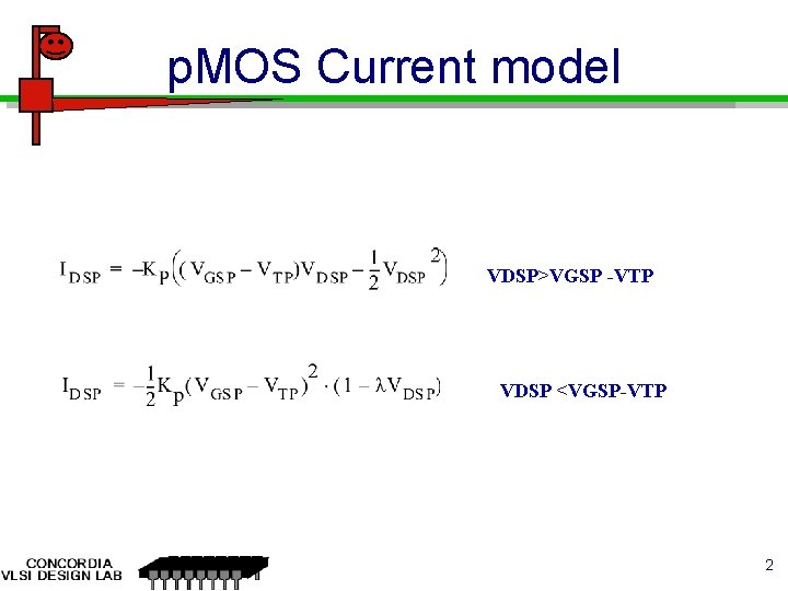
p. MOS Current model VDSP>VGSP -VTP VDSP <VGSP-VTP 2

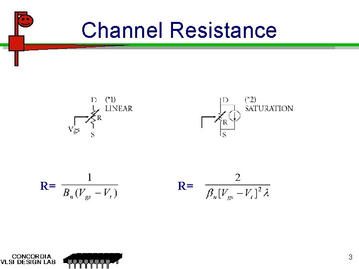
Channel Resistance R= R= 3

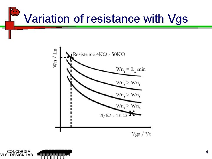
Variation of resistance with Vgs 4

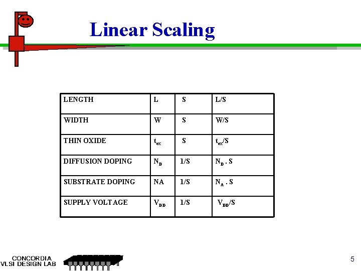
Linear Scaling LENGTH L S L/S WIDTH W S W/S THIN OXIDE tox S tox/S DIFFUSION DOPING ND 1/S ND. S SUBSTRATE DOPING NA 1/S NA. S SUPPLY VOLTAGE VDD 1/S VDD/S 5

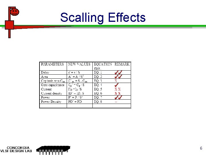
Scalling Effects 6

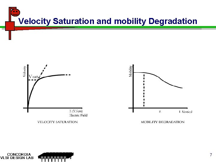
Velocity Saturation and mobility Degradation 7

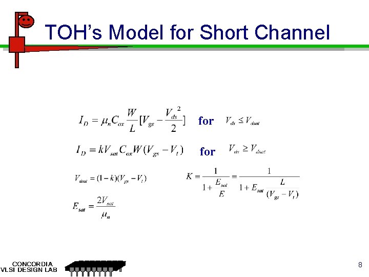
TOH’s Model for Short Channel for 8

Secondary Effects n Subthreshold current: n Punch through: at Vgs < Vt is the small current that flows from drain If a large voltage is applied to Vds, then the depletion region of the drain can extend to the source, a punch through occurs and under these condition a large current can flow from the drain to source. n Hot carrier: As a results of scaling, device dimensions are n Channel hot electrons: If the Vds is increased, then reduced while, doping concentrations are increased, while voltages are not reduced to the same proportion, as a consequence there is an increase in electric field in the channel region while, the thickness of the gate insulating layer is thinner. Due to the acceleration of electrons by the Vds, electrons and holes gaining high speed can penetrate the gate insulator and change its characteristics. the lateral electric field is increased and the electric field accelerates the electrons near the drain with high kinetic energy they are injected into the oxide near the drain. 9

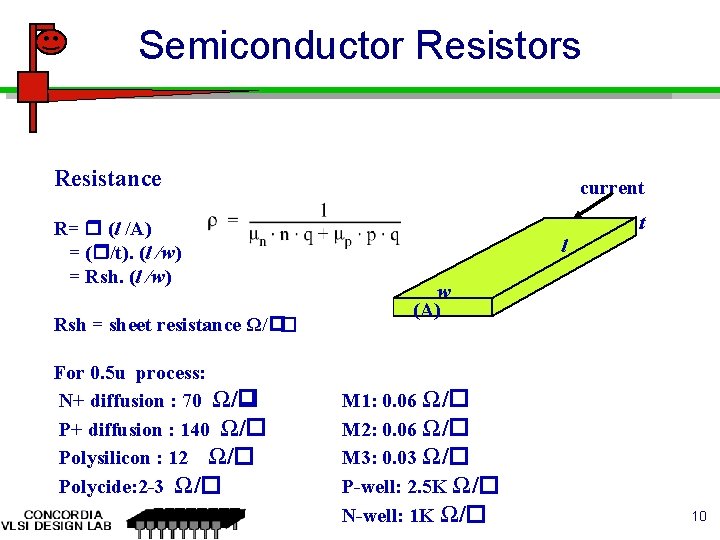
Semiconductor Resistors Resistance R= (l /A) = ( /t). (l /w) = Rsh. (l /w) Rsh = sheet resistance Ω/ For 0. 5 u process: N+ diffusion : 70 Ω/ P+ diffusion : 140 Ω/ Polysilicon : 12 Ω/ Polycide: 2 -3 Ω/ current t l w (A) M 1: 0. 06 Ω/ M 2: 0. 06 Ω/ M 3: 0. 03 Ω/ P-well: 2. 5 K Ω/ N-well: 1 K Ω/ 10

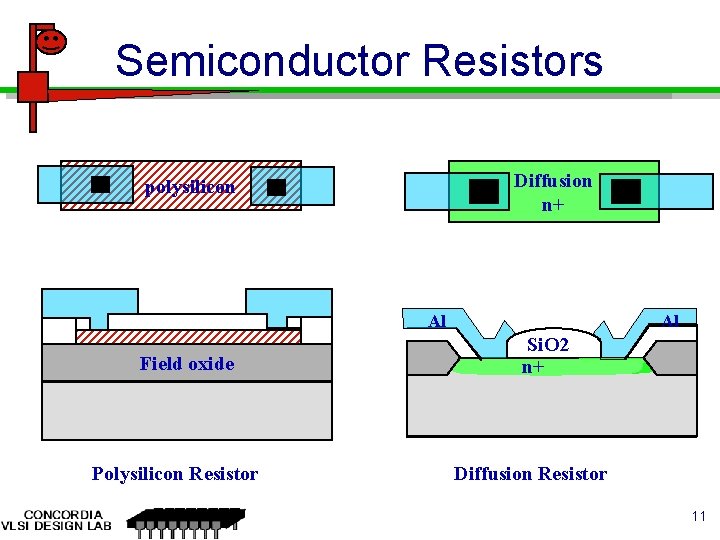
Semiconductor Resistors Diffusion n+ polysilicon Al Field oxide Polysilicon Resistor Al Si. O 2 n+ Diffusion Resistor 11

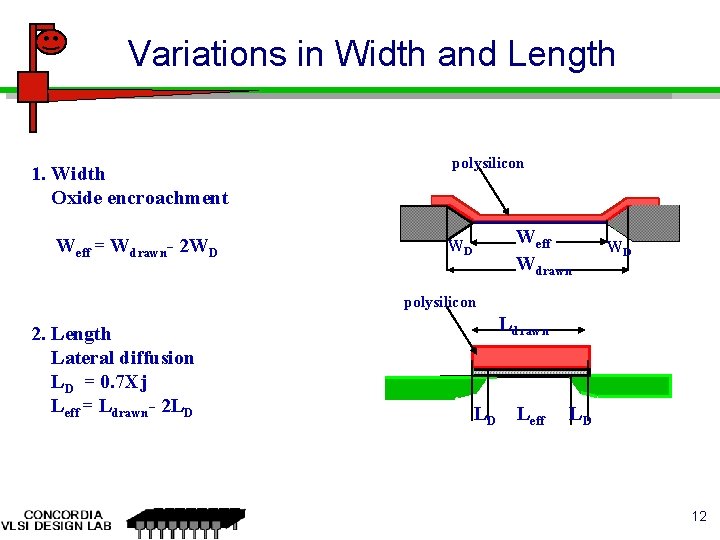
Variations in Width and Length 1. Width Oxide encroachment Weff = Wdrawn- 2 WD polysilicon Weff Wdrawn WD WD polysilicon 2. Length Lateral diffusion LD = 0. 7 Xj Leff = Ldrawn- 2 LD Ldrawn LD Leff LD 12

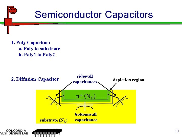
Semiconductor Capacitors 1. Poly Capacitor: a. Poly to substrate b. Poly 1 to Poly 2 2. Diffusion Capacitor sidewall capacitances depletion region n+ (ND) substrate (NA) bottomwall capacitance 13

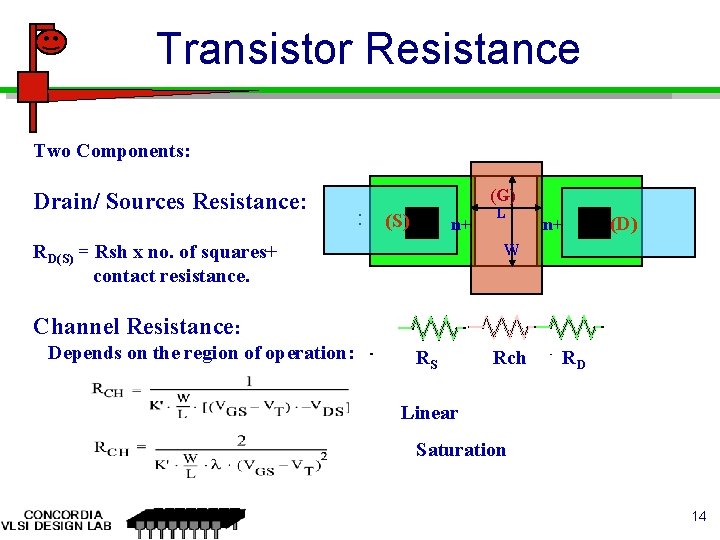
Transistor Resistance Two Components: Drain/ Sources Resistance: (G) : (S) n+ RD(S) = Rsh x no. of squares+ contact resistance. L n+ (D) W Channel Resistance: Depends on the region of operation: RS Rch RD Linear Saturation 14

Dynamic Behavior of MOS Transistor 15 Prentice Hall/Rabaey

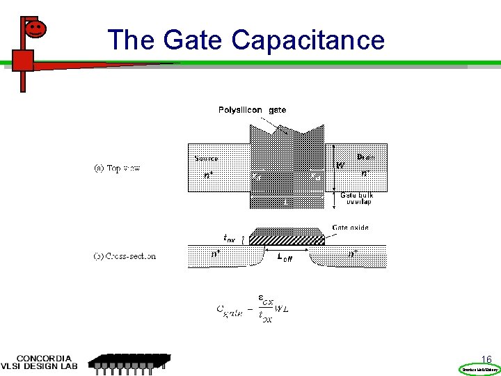
The Gate Capacitance 16 Prentice Hall/Rabaey

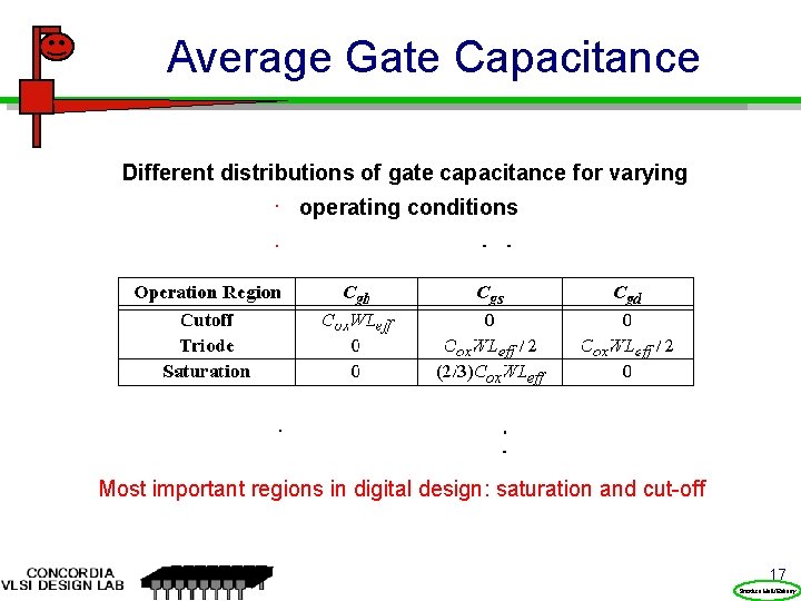
Average Gate Capacitance Different distributions of gate capacitance for varying operating conditions Most important regions in digital design: saturation and cut-off 17 Prentice Hall/Rabaey

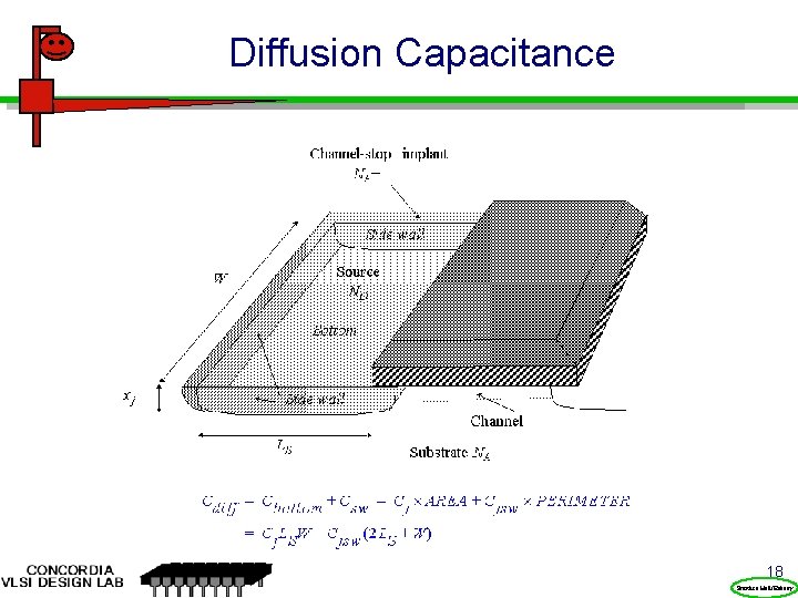
Diffusion Capacitance 18 Prentice Hall/Rabaey

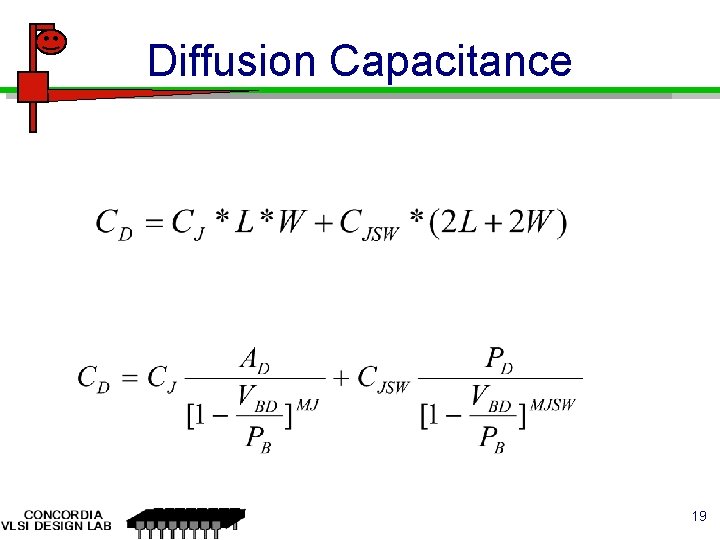
Diffusion Capacitance 19

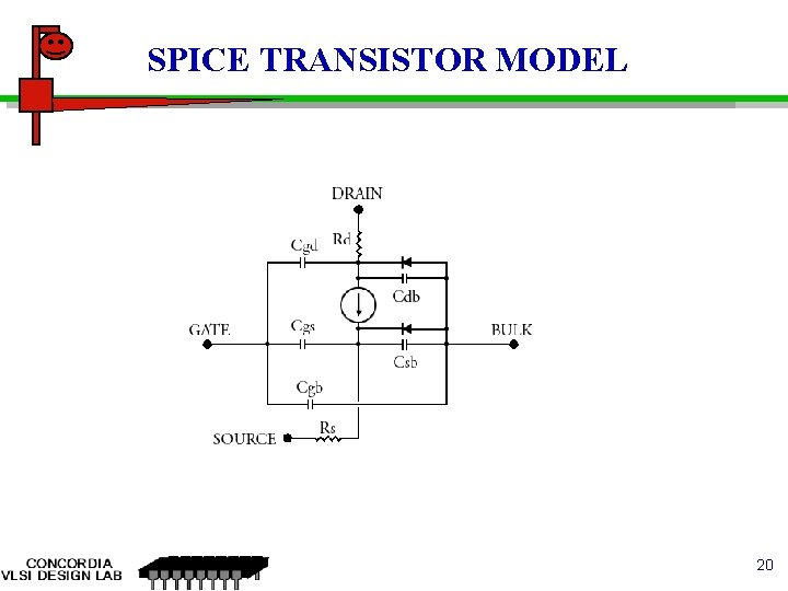
SPICE TRANSISTOR MODEL 20

SPICE MODELS 21

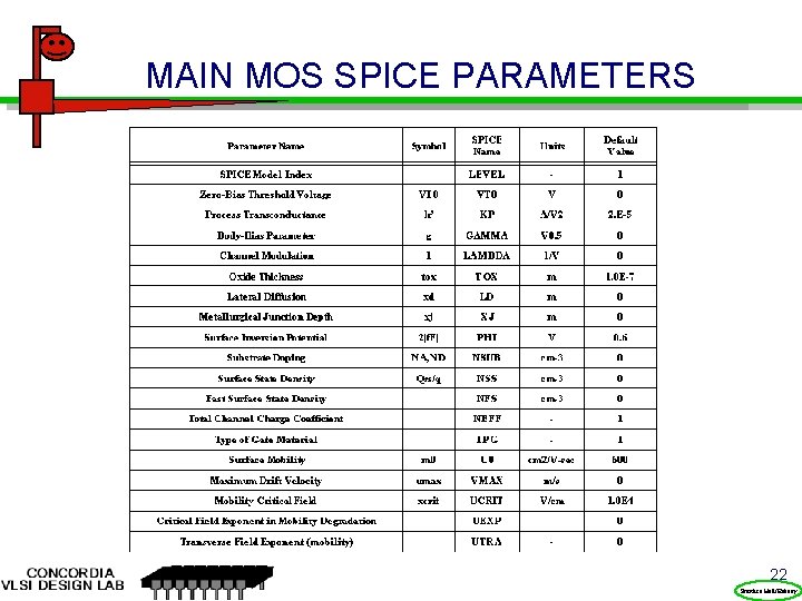
MAIN MOS SPICE PARAMETERS 22 Prentice Hall/Rabaey

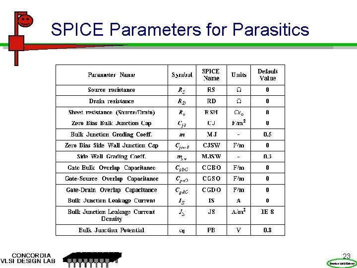
SPICE Parameters for Parasitics 23 Prentice Hall/Rabaey

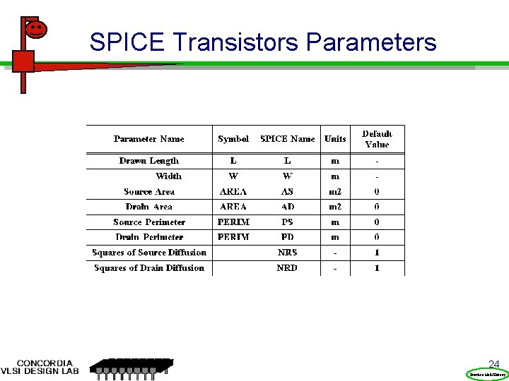
SPICE Transistors Parameters 24 Prentice Hall/Rabaey

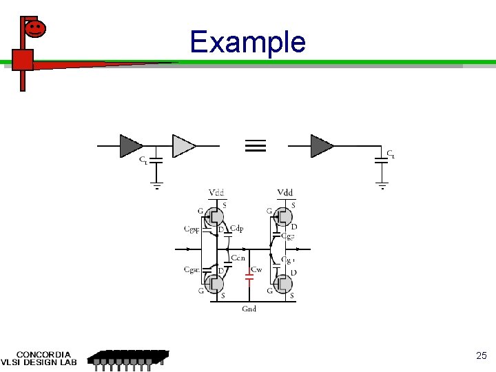
Example 25