Logic and Computer Design Fundamentals Chapter 5 Digital
- Slides: 41

Logic and Computer Design Fundamentals Chapter 5 – Digital Hardware Implementation Charles Kime & Thomas Kaminski © Pearson Education, Inc.

Overview § The Design Space • Integrated Circuits § Levels of Integration • CMOS Circuit Technology § § CMOS Transistor Models Circuits of Switches Fully Complementary CMOS Circuits Technology Parameters § Programmable Implementation Technologies • • • Why Programmable Logic? Programming Technologies Read-Only Memories (ROMs) Programmable Logic Arrays (PLAs) Programmable Array Logic (PALs) © Pearson Education, Inc. Chapter 5 2

5 -1 The Design Space Integrated Circuits § Integrated circuit (informally, a “chip”) is a semiconductor crystal (most often silicon) containing the electronic components for the digital gates and storage elements which are interconnected on the chip. § Terminology - Levels of chip integration • • SSI (small-scale integrated) - fewer than 10 gates MSI (medium-scale integrated) - 10 to 100 gates LSI (large-scale integrated) - 100 to thousands of gates VLSI (very large-scale integrated) - thousands to 100 s of millions of gates © Pearson Education, Inc. Chapter 5 3

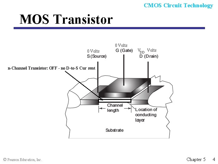
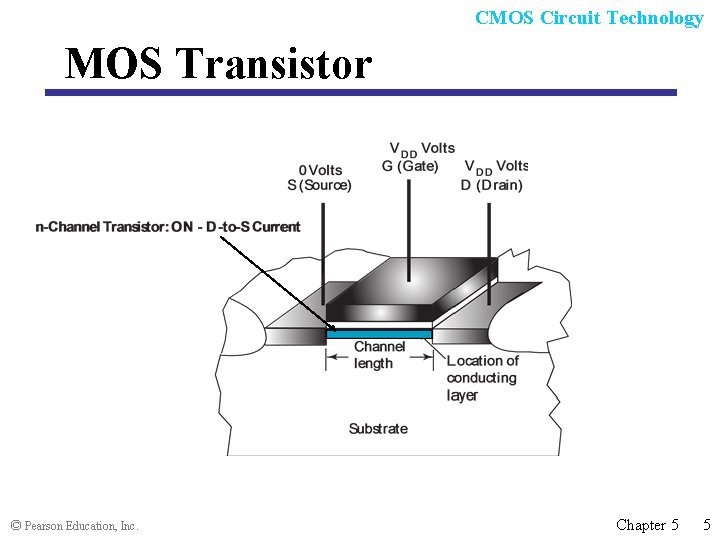
CMOS Circuit Technology MOS Transistor 0 Volts VDD Volts n-Channel Transistor: OFF - no D-to-S Cur rent © Pearson Education, Inc. Chapter 5 4

CMOS Circuit Technology MOS Transistor © Pearson Education, Inc. Chapter 5 5

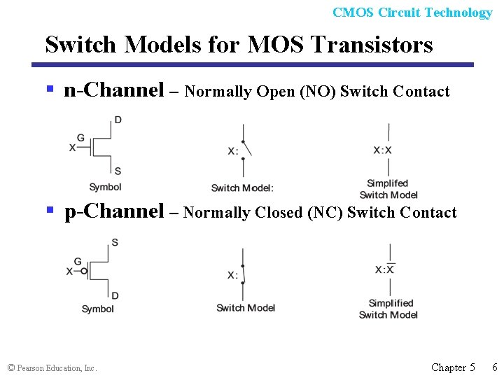
CMOS Circuit Technology Switch Models for MOS Transistors § n-Channel – Normally Open (NO) Switch Contact § p-Channel – Normally Closed (NC) Switch Contact © Pearson Education, Inc. Chapter 5 6

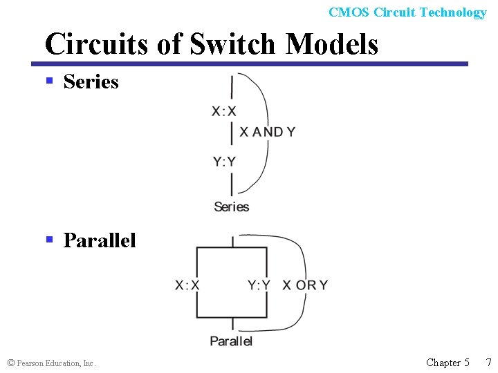
CMOS Circuit Technology Circuits of Switch Models § Series § Parallel © Pearson Education, Inc. Chapter 5 7

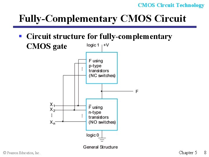
CMOS Circuit Technology Fully-Complementary CMOS Circuit § Circuit structure for fully-complementary CMOS gate © Pearson Education, Inc. Chapter 5 8

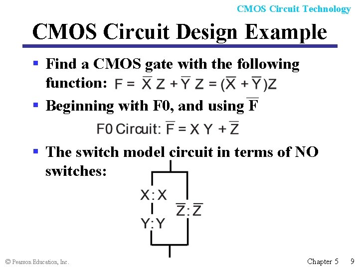
CMOS Circuit Technology CMOS Circuit Design Example § Find a CMOS gate with the following function: § Beginning with F 0, and using F § The switch model circuit in terms of NO switches: © Pearson Education, Inc. Chapter 5 9

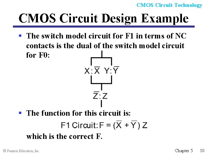
CMOS Circuit Technology CMOS Circuit Design Example § The switch model circuit for F 1 in terms of NC contacts is the dual of the switch model circuit for F 0: § The function for this circuit is: which is the correct F. © Pearson Education, Inc. Chapter 5 10

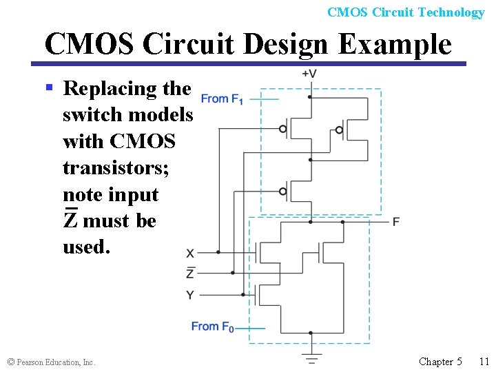
CMOS Circuit Technology CMOS Circuit Design Example § Replacing the switch models with CMOS transistors; note input Z must be used. © Pearson Education, Inc. Chapter 5 11

Technology Parameters § Specific gate implementation technologies are characterized by the following parameters: • Fan-in – the number of inputs available on a gate • Fan-out – the number of standard loads driven by a gate output • Logic Levels – the signal value ranges for 1 and 0 on the inputs and 1 and 0 on the outputs (see Figure 1 -1) • Noise Margin – the maximum external noise voltage superimposed on a normal input value that will not cause an undesirable change in the circuit output • Cost for a gate - a measure of the contribution by the gate to the cost of the integrated circuit • Propagation Delay – The time required for a change in the value of a signal to propagate from an input to an output • Power Dissipation – the amount of power drawn from the power supply and consumed by the gate © Pearson Education, Inc. Chapter 5 12

Technology Parameters Fan-out § Fan-out can be defined in terms of a standard load • Example: 1 standard load equals the load contributed by the input of 1 inverter. • Transition time -the time required for the gate output to change from H to L, t. HL, or from L to H, t. LH • The maximum fan-out that can be driven by a gate is the number of standard loads the gate can drive without exceeding its specified maximum transition time © Pearson Education, Inc. Chapter 5 13

Technology Parameters Cost § In an integrated circuit: • The cost of a gate is proportional to the chip area occupied by the gate • The gate area is roughly proportional to the number and size of the transistors and the amount of wiring connecting them • Ignoring the wiring area, the gate area is roughly proportional to the gate input count • So gate input count is a rough measure of gate cost § If the actual chip layout area occupied by the gate is known, it is a far more accurate measure © Pearson Education, Inc. Chapter 5 14

5 -2 Programmable Implementation Technologies Why Programmable Logic? § Facts: • It is most economical to produce an IC in large volumes • Many designs required only small volumes of ICs § Need an IC that can be: • Produced in large volumes • Handle many designs required in small volumes § A programmable logic part can be: • made in large volumes • programmed to implement large numbers of different low-volume designs © Pearson Education, Inc. Chapter 5 15

5 -2 Programmable Implementation Technologies Programmable Logic - More Advantages § Many programmable logic devices are fieldprogrammable, i. e. , can be programmed outside of the manufacturing environment § Most programmable logic devices are erasable and reprogrammable. • Allows “updating” a device or correction of errors • Allows reuse the device for a different design - the ultimate in re-usability! • Ideal for course laboratories § Programmable logic devices can be used to prototype design that will be implemented for sale in regular ICs. • Complete Intel Pentium designs were actually prototyped with specialized systems based on large numbers of VLSI programmable devices! © Pearson Education, Inc. Chapter 5 16

5 -2 Programmable Implementation Technologies Programming Technologies § Programming technologies are used to: • Control connections • Build lookup tables • Control transistor switching § The technologies • Control connections § Mask programming § Fuse § Antifuse § Single-bit storage element © Pearson Education, Inc. Chapter 5 17

5 -2 Programmable Implementation Technologies Programming Technologies § The technologies (continued) • Build lookup tables § Storage elements (as in a memory) • Transistor Switching Control § Stored charge on a floating transistor gate • Erasable • Electrically erasable • Flash (as in Flash Memory) © Pearson Education, Inc. Chapter 5 18

5 -2 Programmable Implementation Technologies Technology Characteristics § Permanent - Cannot be erased and reprogrammed § Mask programming § Fuse § Antifuse § Reprogrammable • Volatile - Programming lost if chip power lost § Single-bit storage element • Non-Volatile § Erasable § Electrically erasable § Flash (as in Flash Memory) © Pearson Education, Inc. Chapter 5 19

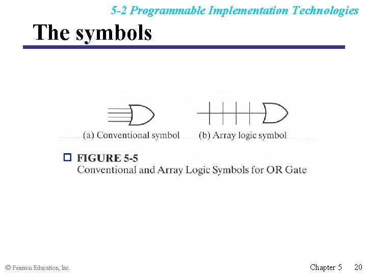
5 -2 Programmable Implementation Technologies The symbols © Pearson Education, Inc. Chapter 5 20

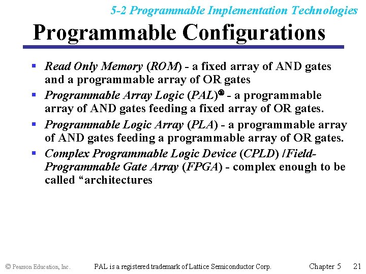
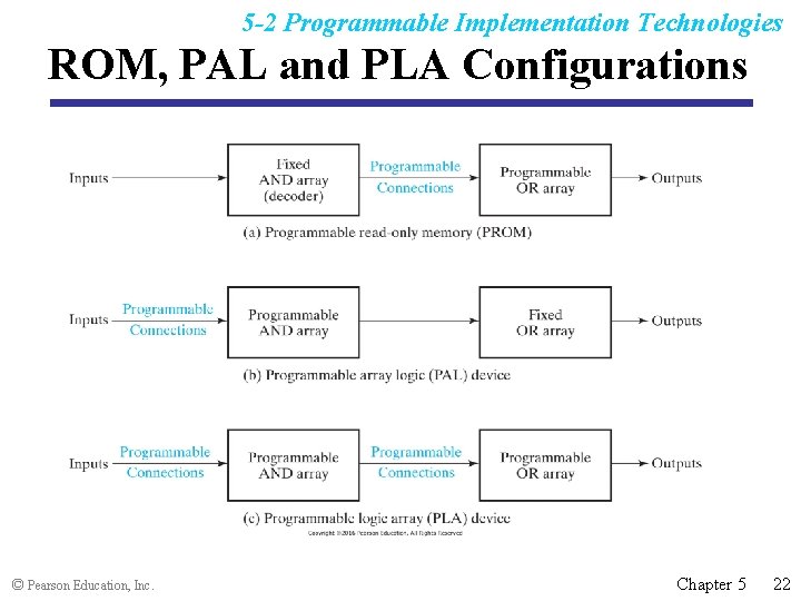
5 -2 Programmable Implementation Technologies Programmable Configurations § Read Only Memory (ROM) - a fixed array of AND gates and a programmable array of OR gates § Programmable Array Logic (PAL)Ò - a programmable array of AND gates feeding a fixed array of OR gates. § Programmable Logic Array (PLA) - a programmable array of AND gates feeding a programmable array of OR gates. § Complex Programmable Logic Device (CPLD) /Field. Programmable Gate Array (FPGA) - complex enough to be called “architectures © Pearson Education, Inc. PAL is a registered trademark of Lattice Semiconductor Corp. Chapter 5 21

5 -2 Programmable Implementation Technologies ROM, PAL and PLA Configurations © Pearson Education, Inc. Chapter 5 22

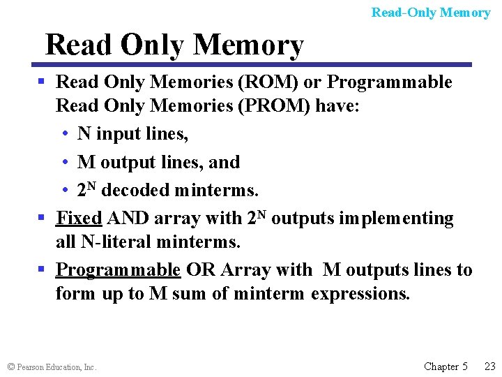
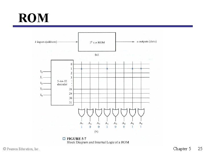
Read-Only Memory Read Only Memory § Read Only Memories (ROM) or Programmable Read Only Memories (PROM) have: • N input lines, • M output lines, and • 2 N decoded minterms. § Fixed AND array with 2 N outputs implementing all N-literal minterms. § Programmable OR Array with M outputs lines to form up to M sum of minterm expressions. © Pearson Education, Inc. Chapter 5 23

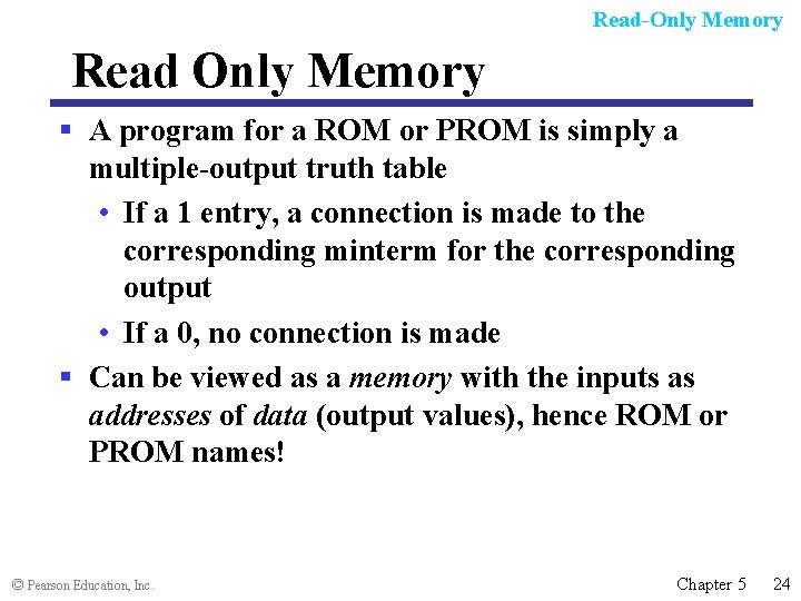
Read-Only Memory Read Only Memory § A program for a ROM or PROM is simply a multiple-output truth table • If a 1 entry, a connection is made to the corresponding minterm for the corresponding output • If a 0, no connection is made § Can be viewed as a memory with the inputs as addresses of data (output values), hence ROM or PROM names! © Pearson Education, Inc. Chapter 5 24

ROM © Pearson Education, Inc. Chapter 5 25

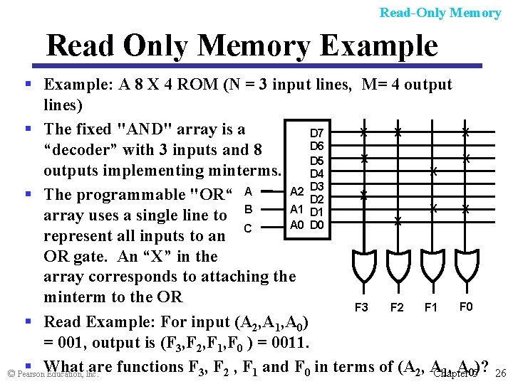
Read-Only Memory Read Only Memory Example § Example: A 8 X 4 ROM (N = 3 input lines, M= 4 output lines) § The fixed "AND" array is a X X X D 7 D 6 “decoder” with 3 inputs and 8 X X D 5 X outputs implementing minterms. D 4 A 2 D 3 X § The programmable "OR“ A D 2 X X A 1 D 1 array uses a single line to B X A 0 D 0 C represent all inputs to an OR gate. An “X” in the array corresponds to attaching the minterm to the OR F 0 F 2 F 1 F 3 § Read Example: For input (A 2, A 1, A 0) = 001, output is (F 3, F 2, F 1, F 0 ) = 0011. § What are functions F 3, F 2 , F 1 and F 0 in terms of (A 2, A 1, A 05)? © Pearson Education, Inc. Chapter 26

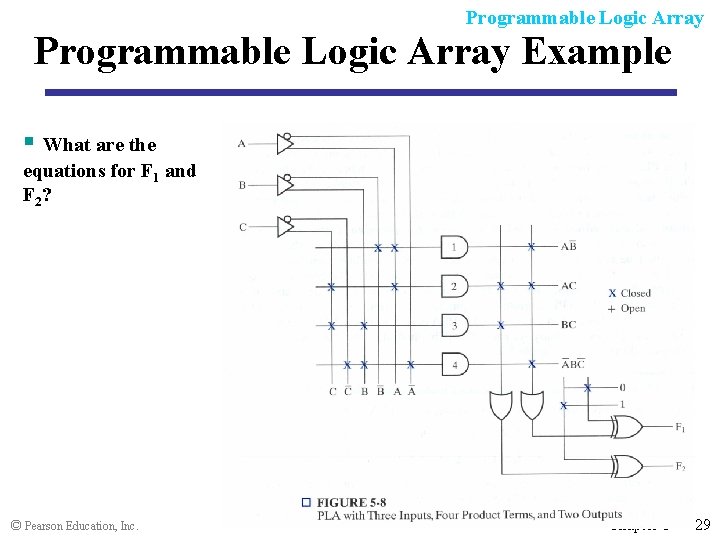
Programmable Logic Array (PLA) § Compared to a ROM and a PAL, a PLA is the most flexible having a programmable set of ANDs combined with a programmable set of ORs. § Advantages • A PLA can have large N and M permitting implementation of equations that are impractical for a ROM (because of the number of inputs, N, required • A PLA has all of its product terms connectable to all outputs, overcoming the problem of the limited inputs to the PAL Ors • Some PLAs have outputs that can be complemented, adding POS functions © Pearson Education, Inc. Chapter 5 27

Programmable Logic Array (PLA) § Disadvantages • Often, the product term count limits the application of a PLA. • Two-level multiple-output optimization is required to reduce the number of product terms in an implementation, helping to fit it into a PLA. • Multi-level circuit capability available in PAL not available in PLA requires external connections to do multi-level circuits. © Pearson Education, Inc. Chapter 5 28

Programmable Logic Array Example § What are the equations for F 1 and F 2 ? © Pearson Education, Inc. Chapter 5 29

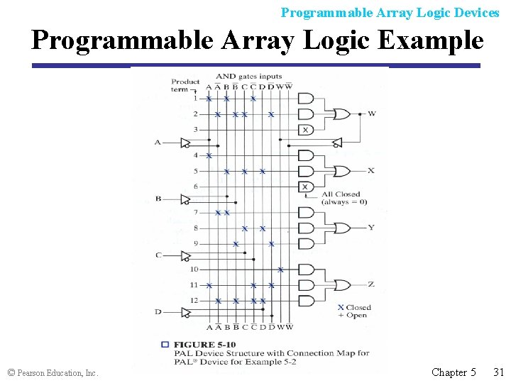
Programmable Array Logic Devices Programmable Array Logic (PAL) § The PAL is the opposite of the ROM, having a programmable set of ANDs combined with fixed ORs. § Disadvantage • ROM guaranteed to implement any M functions of N inputs. PAL may have too few inputs to the OR gates. § Advantages • For given internal complexity, a PAL can have larger N and M • Some PALs have outputs that can be complemented, adding POS functions • No multilevel circuit implementations in ROM (without external connections from output to input). PAL has outputs from OR terms as internal inputs to all AND terms, making implementation of multi-level circuits easier. © Pearson Education, Inc. Chapter 5 30

Programmable Array Logic Devices Programmable Array Logic Example © Pearson Education, Inc. Chapter 5 31

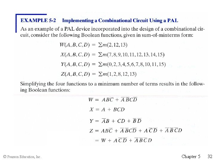
© Pearson Education, Inc. Chapter 5 32

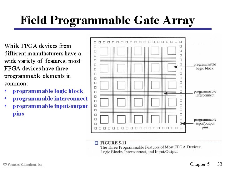
Field Programmable Gate Array While FPGA devices from different manufacturers have a wide variety of features, most FPGA devices have three programmable elements in common: • programmable logic block • programmable interconnect • programmable input/output pins © Pearson Education, Inc. Chapter 5 33

Programmable logic block § © Pearson Education, Inc. Chapter 5 34

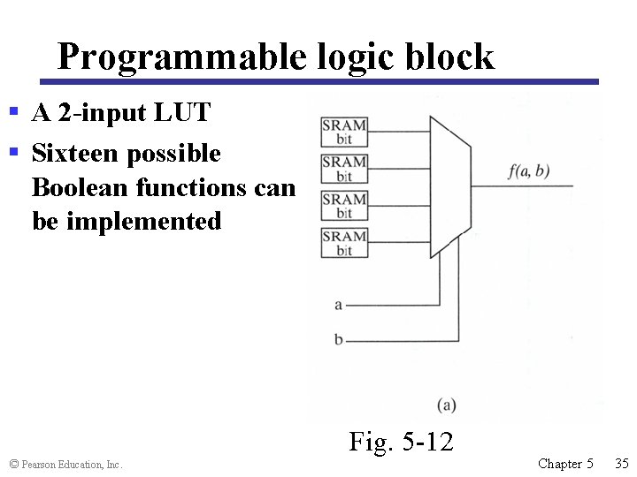
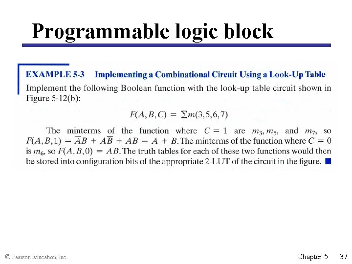
Programmable logic block § A 2 -input LUT § Sixteen possible Boolean functions can be implemented Fig. 5 -12 © Pearson Education, Inc. Chapter 5 35

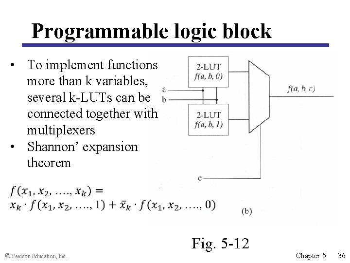
Programmable logic block • To implement functions more than k variables, several k-LUTs can be connected together with multiplexers • Shannon’ expansion theorem Fig. 5 -12 © Pearson Education, Inc. Chapter 5 36

Programmable logic block © Pearson Education, Inc. Chapter 5 37

Programmable logic block In addition to LUT, there are § Multiplexers § Flip-flops § Other logic to configure the block to implement a wide variety of functions © Pearson Education, Inc. Chapter 5 38

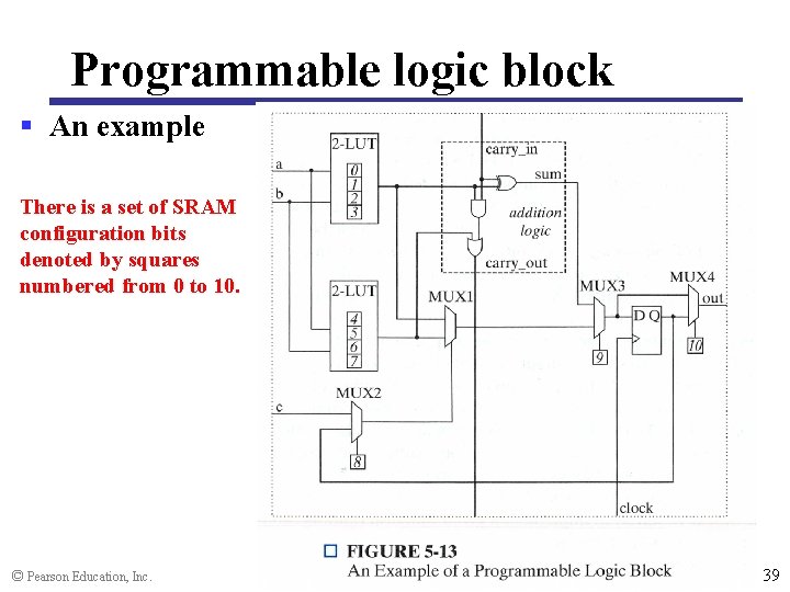
Programmable logic block § An example There is a set of SRAM configuration bits denoted by squares numbered from 0 to 10. © Pearson Education, Inc. Chapter 5 39

Programmable interconnection § is made up of a set of wires and programmable switches § programmable switches usually consists of a single n-channel MOS transistor © Pearson Education, Inc. Chapter 5 40

Programmable input/output (I/O) pins § The FPGA must be connected with the outside world § Must be compatible with the speed and voltage requirements of the other electrical components to which it will be connected. § Most FPGAs provide a large number of pins that can be configured to support a number of different electrical interface standards. © Pearson Education, Inc. Chapter 5 41