Digital Fundamentals Tenth Edition Floyd Chapter 9 Floyd

- Slides: 36

Digital Fundamentals Tenth Edition Floyd Chapter 9 Floyd, Digital Fundamentals, 10 th ed 2008 Pearson Education © 2009 Pearson Education, ©Upper Saddle River, NJ 07458. All Rights Reserved

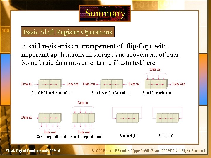
Summary Basic Shift Register Operations A shift register is an arrangement of flip-flops with important applications in storage and movement of data. Some basic data movements are illustrated here. Data in Data out Serial in/shift right/serial out Data in Serial in/shift left/serial out Data out Parallel in/serial out Data in Data out Serial in/parallel out Floyd, Digital Fundamentals, 10 th ed Data out Parallel in/parallel out Rotate right Rotate left © 2009 Pearson Education, Upper Saddle River, NJ 07458. All Rights Reserved

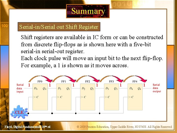
Summary Serial-in/Serial out Shift Register Shift registers are available in IC form or can be constructed from discrete flip-flops as is shown here with a five-bit serial-in serial-out register. Each clock pulse will move an input bit to the next flip-flop. For example, a 1 is shown as it moves across. 1 1 1 CLK Floyd, Digital Fundamentals, 10 th ed © 2009 Pearson Education, Upper Saddle River, NJ 07458. All Rights Reserved

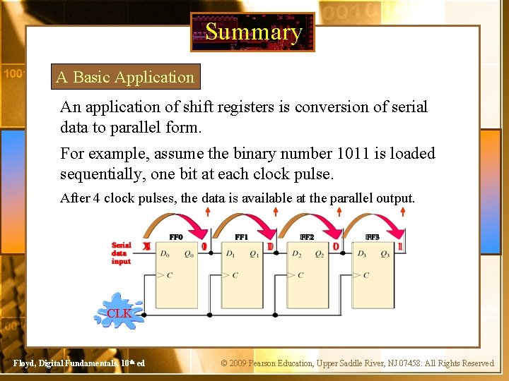
Summary A Basic Application An application of shift registers is conversion of serial data to parallel form. For example, assume the binary number 1011 is loaded sequentially, one bit at each clock pulse. After 4 clock pulses, the data is available at the parallel output. CLK Floyd, Digital Fundamentals, 10 th ed © 2009 Pearson Education, Upper Saddle River, NJ 07458. All Rights Reserved

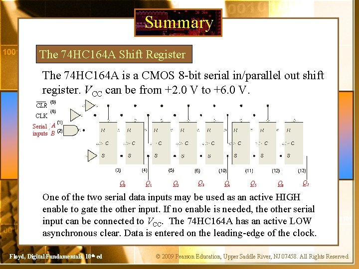
Summary The 74 HC 164 A Shift Register The 74 HC 164 A is a CMOS 8 -bit serial in/parallel out shift register. VCC can be from +2. 0 V to +6. 0 V. CLR CLK Serial A inputs B Q 0 Q 1 Q 2 Q 3 Q 4 Q 5 Q 6 Q 7 One of the two serial data inputs may be used as an active HIGH enable to gate the other input. If no enable is needed, the other serial input can be connected to VCC. The 74 HC 164 A has an active LOW asynchronous clear. Data is entered on the leading-edge of the clock. Floyd, Digital Fundamentals, 10 th ed © 2009 Pearson Education, Upper Saddle River, NJ 07458. All Rights Reserved

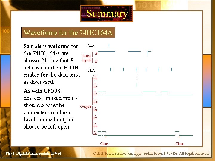
Summary Waveforms for the 74 HC 164 A Sample waveforms for the 74 HC 164 A are shown. Notice that B acts as an active HIGH enable for the data on A as discussed. As with CMOS devices, unused inputs should always be connected to a logic level; unused outputs should be left open. CLR A Serial inputs B CLK Q 0 Q 1 Q 2 Q 3 Outputs Q 4 Q 5 Q 6 Q 7 Clear Floyd, Digital Fundamentals, 10 th ed Clear © 2009 Pearson Education, Upper Saddle River, NJ 07458. All Rights Reserved

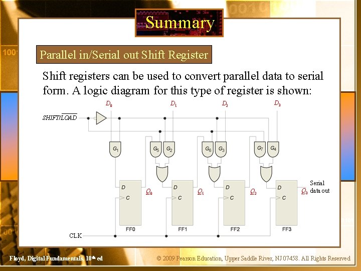
Summary Parallel in/Serial out Shift Register Shift registers can be used to convert parallel data to serial form. A logic diagram for this type of register is shown: D 0 D 1 D 3 D 2 SHIFT/LOAD Q 0 Q 1 Q 2 Serial Q 3 data out CLK Floyd, Digital Fundamentals, 10 th ed © 2009 Pearson Education, Upper Saddle River, NJ 07458. All Rights Reserved

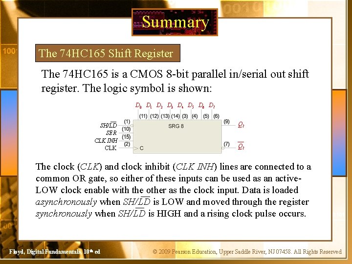
Summary The 74 HC 165 Shift Register The 74 HC 165 is a CMOS 8 -bit parallel in/serial out shift register. The logic symbol is shown: D 0 D 1 D 2 D 3 D 4 D 5 D 6 D 7 SH/LD SER CLK INH CLK Q 7 The clock (CLK) and clock inhibit (CLK INH) lines are connected to a common OR gate, so either of these inputs can be used as an active. LOW clock enable with the other as the clock input. Data is loaded asynchronously when SH/LD is LOW and moved through the register synchronously when SH/LD is HIGH and a rising clock pulse occurs. Floyd, Digital Fundamentals, 10 th ed © 2009 Pearson Education, Upper Saddle River, NJ 07458. All Rights Reserved

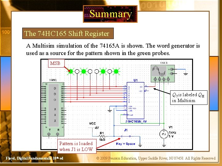
Summary The 74 HC 165 Shift Register A Multisim simulation of the 74165 A is shown. The word generator is used as a source for the pattern shown in the green probes. MSB Q 7 is labeled QH in Multisim Pattern is loaded when J 1 is LOW Floyd, Digital Fundamentals, 10 th ed © 2009 Pearson Education, Upper Saddle River, NJ 07458. All Rights Reserved

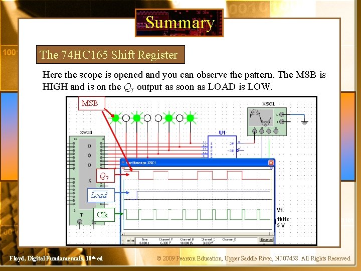
Summary The 74 HC 165 Shift Register Here the scope is opened and you can observe the pattern. The MSB is HIGH and is on the Q 7 output as soon as LOAD is LOW. MSB Q 7 Load Clk Floyd, Digital Fundamentals, 10 th ed © 2009 Pearson Education, Upper Saddle River, NJ 07458. All Rights Reserved

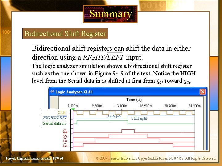
Summary Bidirectional Shift Register Bidirectional shift registers can shift the data in either direction using a RIGHT/LEFT input. The logic analyzer simulation shows a bidirectional shift register such as the one shown in Figure 9 -19 of the text. Notice the HIGH level from the Serial data in is shifted at first from Q 3 toward Q 0. CLK RIGHT/LEFT Serial data in Shift left Shift right Q 0 Q 1 Q 2 Q 3 Floyd, Digital Fundamentals, 10 th ed © 2009 Pearson Education, Upper Saddle River, NJ 07458. All Rights Reserved

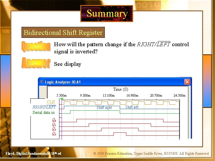
Summary Bidirectional Shift Register How will the pattern change if the RIGHT/LEFT control signal is inverted? See display CLK RIGHT/LEFT Serial data in Shiftleft right Shift right left Q 0 Q 1 Q 2 Q 3 Floyd, Digital Fundamentals, 10 th ed © 2009 Pearson Education, Upper Saddle River, NJ 07458. All Rights Reserved

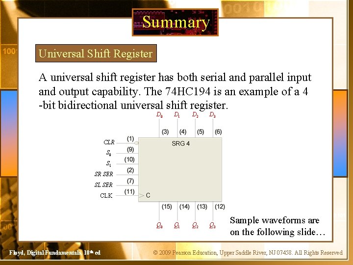
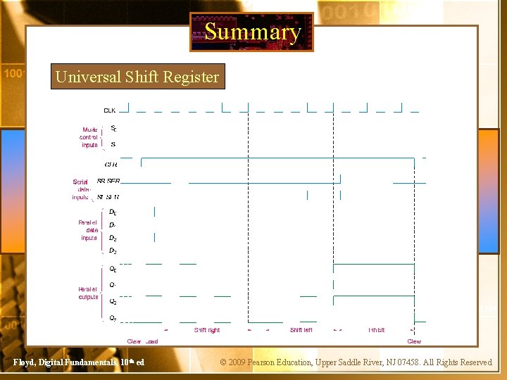
Summary Universal Shift Register A universal shift register has both serial and parallel input and output capability. The 74 HC 194 is an example of a 4 -bit bidirectional universal shift register. D 0 D 1 D 2 D 3 Q 0 Q 1 Q 2 Q 3 CLR S 0 S 1 SR SER SL SER CLK Floyd, Digital Fundamentals, 10 th ed Sample waveforms are on the following slide… © 2009 Pearson Education, Upper Saddle River, NJ 07458. All Rights Reserved

Summary Universal Shift Register Floyd, Digital Fundamentals, 10 th ed © 2009 Pearson Education, Upper Saddle River, NJ 07458. All Rights Reserved

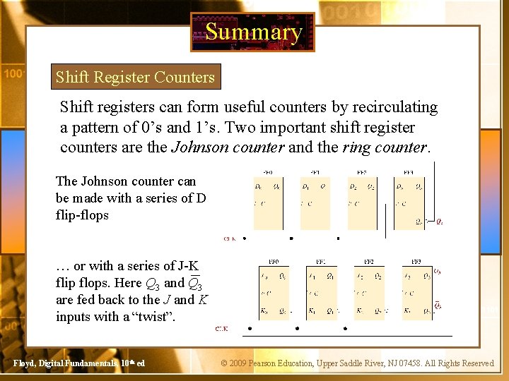
Summary Shift Register Counters Shift registers can form useful counters by recirculating a pattern of 0’s and 1’s. Two important shift register counters are the Johnson counter and the ring counter. The Johnson counter can be made with a series of D flip-flops … or with a series of J-K flip flops. Here Q 3 and Q 3 are fed back to the J and K inputs with a “twist”. Floyd, Digital Fundamentals, 10 th ed © 2009 Pearson Education, Upper Saddle River, NJ 07458. All Rights Reserved

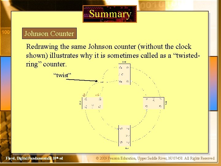
Summary Johnson Counter Redrawing the same Johnson counter (without the clock shown) illustrates why it is sometimes called as a “twistedring” counter. “twist” Floyd, Digital Fundamentals, 10 th ed © 2009 Pearson Education, Upper Saddle River, NJ 07458. All Rights Reserved

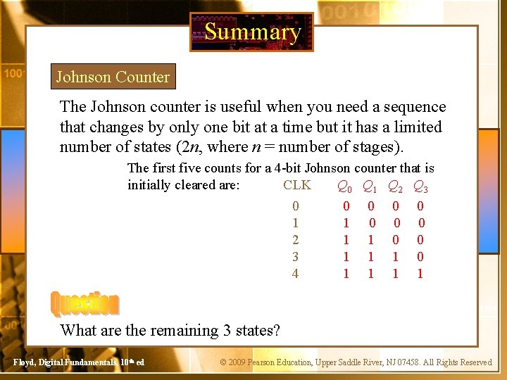
Summary Johnson Counter The Johnson counter is useful when you need a sequence that changes by only one bit at a time but it has a limited number of states (2 n, where n = number of stages). The first five counts for a 4 -bit Johnson counter that is initially cleared are: CLK Q 0 Q 1 Q 2 Q 3 What are the remaining 3 states? Floyd, Digital Fundamentals, 10 th ed 0 1 2 3 4 5 6 7 0 1 1 1 1 0 0 0 0 0 1 1 © 2009 Pearson Education, Upper Saddle River, NJ 07458. All Rights Reserved

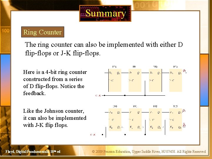
Summary Ring Counter The ring counter can also be implemented with either D flip-flops or J-K flip-flops. Here is a 4 -bit ring counter constructed from a series of D flip-flops. Notice the feedback. Like the Johnson counter, it can also be implemented with J-K flip flops. Floyd, Digital Fundamentals, 10 th ed © 2009 Pearson Education, Upper Saddle River, NJ 07458. All Rights Reserved

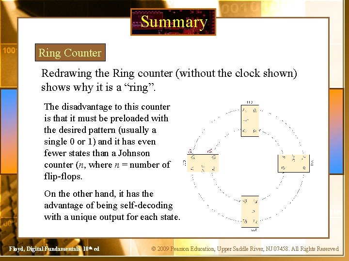
Summary Ring Counter Redrawing the Ring counter (without the clock shown) shows why it is a “ring”. The disadvantage to this counter is that it must be preloaded with the desired pattern (usually a single 0 or 1) and it has even fewer states than a Johnson counter (n, where n = number of flip-flops. On the other hand, it has the advantage of being self-decoding with a unique output for each state. Floyd, Digital Fundamentals, 10 th ed © 2009 Pearson Education, Upper Saddle River, NJ 07458. All Rights Reserved

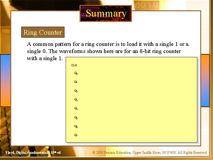
Summary Ring Counter A common pattern for a ring counter is to load it with a single 1 or a single 0. The waveforms shown here are for an 8 -bit ring counter with a single 1. Floyd, Digital Fundamentals, 10 th ed © 2009 Pearson Education, Upper Saddle River, NJ 07458. All Rights Reserved

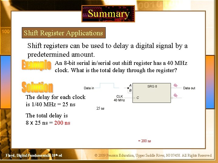
Summary Shift Register Applications Shift registers can be used to delay a digital signal by a predetermined amount. An 8 -bit serial in/serial out shift register has a 40 MHz clock. What is the total delay through the register? The delay for each clock is 1/40 MHz = 25 ns The total delay is 8 x 25 ns = 200 ns Floyd, Digital Fundamentals, 10 th ed © 2009 Pearson Education, Upper Saddle River, NJ 07458. All Rights Reserved

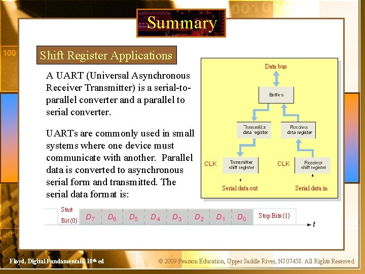
Summary Shift Register Applications Data bus A UART (Universal Asynchronous Receiver Transmitter) is a serial-toparallel converter and a parallel to serial converter. UARTs are commonly used in small systems where one device must communicate with another. Parallel data is converted to asynchronous serial form and transmitted. The serial data format is: Start Bit (0) Floyd, Digital Fundamentals, 10 th ed CLK Serial data out Serial data in Stop Bits (1) © 2009 Pearson Education, Upper Saddle River, NJ 07458. All Rights Reserved

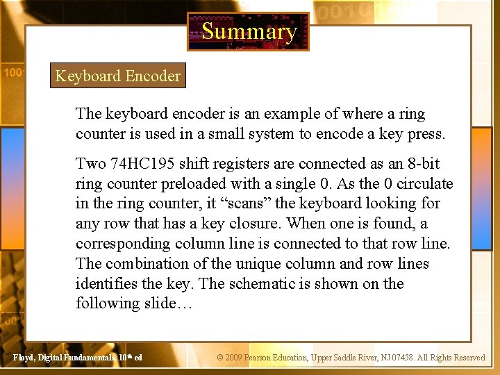
Summary Keyboard Encoder The keyboard encoder is an example of where a ring counter is used in a small system to encode a key press. Two 74 HC 195 shift registers are connected as an 8 -bit ring counter preloaded with a single 0. As the 0 circulate in the ring counter, it “scans” the keyboard looking for any row that has a key closure. When one is found, a corresponding column line is connected to that row line. The combination of the unique column and row lines identifies the key. The schematic is shown on the following slide… Floyd, Digital Fundamentals, 10 th ed © 2009 Pearson Education, Upper Saddle River, NJ 07458. All Rights Reserved

Floyd, Digital Fundamentals, 10 th ed © 2009 Pearson Education, Upper Saddle River, NJ © 07458. 2008 All Pearson Rights. Education Reserved

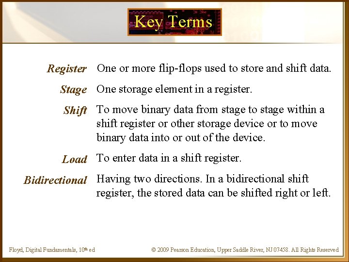
Key Terms Register One or more flip-flops used to store and shift data. Stage One storage element in a register. Shift To move binary data from stage to stage within a shift register or other storage device or to move binary data into or out of the device. Load To enter data in a shift register. Bidirectional Having two directions. In a bidirectional shift register, the stored data can be shifted right or left. Floyd, Digital Fundamentals, 10 th ed © 2009 Pearson Education, Upper Saddle River, NJ 07458. All Rights Reserved

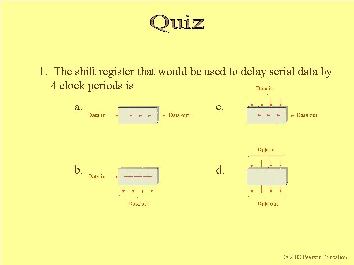
1. The shift register that would be used to delay serial data by 4 clock periods is a. c. b. d. Floyd, Digital Fundamentals, 10 th ed © 2009 Pearson Education, Upper Saddle River, NJ 07458. All Rights Reserved © 2008 Pearson Education

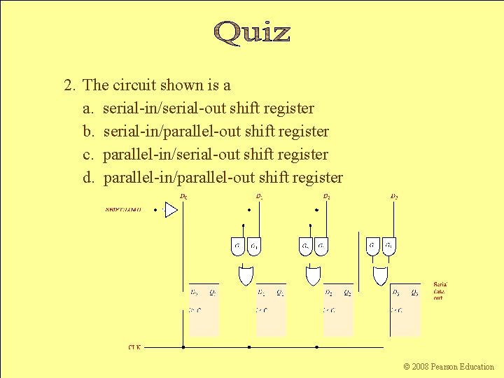
2. The circuit shown is a a. serial-in/serial-out shift register b. serial-in/parallel-out shift register c. parallel-in/serial-out shift register d. parallel-in/parallel-out shift register Floyd, Digital Fundamentals, 10 th ed © 2009 Pearson Education, Upper Saddle River, NJ 07458. All Rights Reserved © 2008 Pearson Education

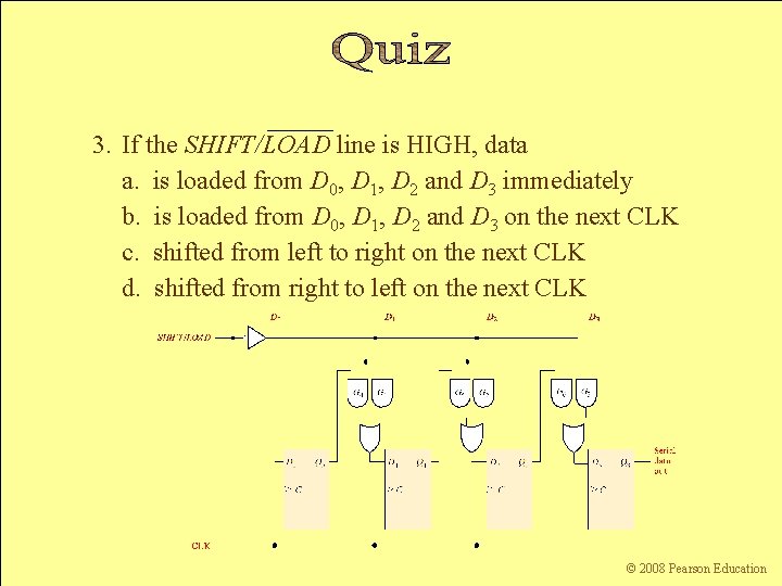
3. If the SHIFT/LOAD line is HIGH, data a. is loaded from D 0, D 1, D 2 and D 3 immediately b. is loaded from D 0, D 1, D 2 and D 3 on the next CLK c. shifted from left to right on the next CLK d. shifted from right to left on the next CLK Floyd, Digital Fundamentals, 10 th ed © 2009 Pearson Education, Upper Saddle River, NJ 07458. All Rights Reserved © 2008 Pearson Education

4. A 4 -bit parallel-in/parallel-out shift register will store data for a. 1 clock period b. 2 clock periods c. 3 clock periods d. 4 clock periods Floyd, Digital Fundamentals, 10 th ed © 2009 Pearson Education, Upper Saddle River, NJ 07458. All Rights Reserved © 2008 Pearson Education

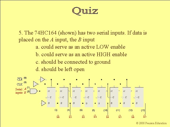
5. The 74 HC 164 (shown) has two serial inputs. If data is placed on the A input, the B input a. could serve as an active LOW enable b. could serve as an active HIGH enable c. should be connected to ground d. should be left open CLR CLK Serial A inputs B Q 0 Floyd, Digital Fundamentals, 10 th ed Q 1 Q 2 Q 3 Q 4 Q 5 Q 6 Q 7 © 2009 Pearson Education, Upper Saddle River, NJ 07458. All Rights Reserved © 2008 Pearson Education

6. An advantage of a ring counter over a Johnson counter is that the ring counter a. has more possible states for a given number of flip-flops b. is cleared after each cycle c. allows only one bit to change at a time d. is self-decoding Floyd, Digital Fundamentals, 10 th ed © 2009 Pearson Education, Upper Saddle River, NJ 07458. All Rights Reserved

7. A possible sequence for a 4 -bit ring counter is a. … 1111, 1110, 1101 … b. … 0000, 0001, 0010 … c. … 0001, 0011, 0111 … d. … 1000, 0100, 0010 … Floyd, Digital Fundamentals, 10 th ed © 2009 Pearson Education, Upper Saddle River, NJ 07458. All Rights Reserved

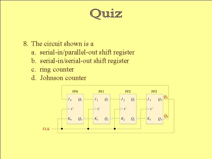
8. The circuit shown is a a. serial-in/parallel-out shift register b. serial-in/serial-out shift register c. ring counter d. Johnson counter Floyd, Digital Fundamentals, 10 th ed © 2009 Pearson Education, Upper Saddle River, NJ 07458. All Rights Reserved

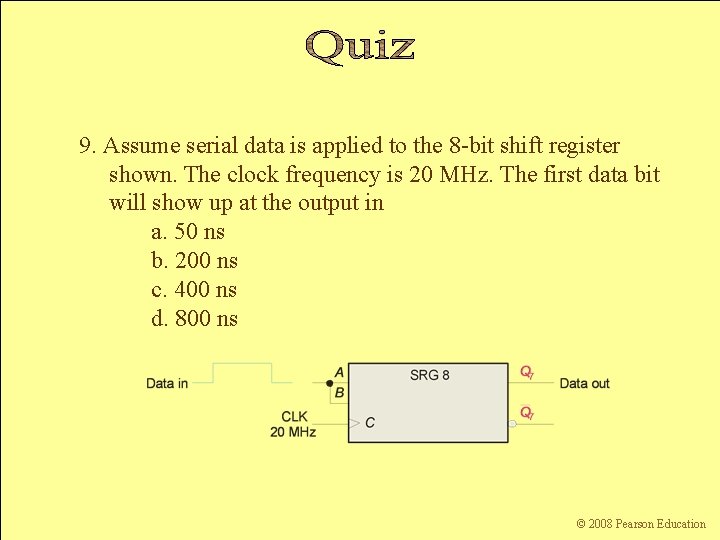
9. Assume serial data is applied to the 8 -bit shift register shown. The clock frequency is 20 MHz. The first data bit will show up at the output in a. 50 ns b. 200 ns c. 400 ns d. 800 ns Floyd, Digital Fundamentals, 10 th ed © 2009 Pearson Education, Upper Saddle River, NJ 07458. All Rights Reserved © 2008 Pearson Education

10. For transmission, data from a UART is sent in a. asynchronous serial form b. synchronous parallel form c. can be either of the above d. none of the above Floyd, Digital Fundamentals, 10 th ed © 2009 Pearson Education, Upper Saddle River, NJ 07458. All Rights Reserved © 2008 Pearson Education

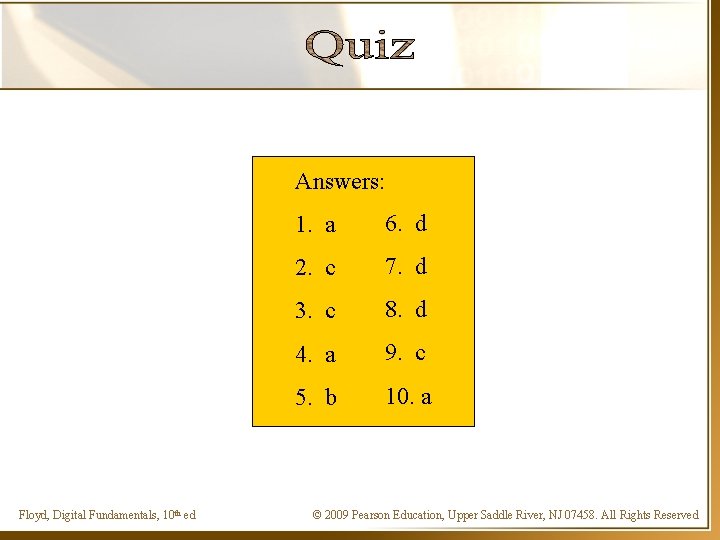
Answers: Floyd, Digital Fundamentals, 10 th ed 1. a 6. d 2. c 7. d 3. c 8. d 4. a 9. c 5. b 10. a © 2009 Pearson Education, Upper Saddle River, NJ 07458. All Rights Reserved