GPU Memory Hierarchy Optimizations Carlos Gonzlez Rodrguez Advisors




- Slides: 37

GPU Memory Hierarchy Optimizations Carlos González Rodríguez Advisors: Roger Espasa and Agustín Fernández Departament d’Arquitectura de Computadors (DAC) Universitat Politècnica de Catalunya (UPC) June 2007

Contents Today’s GPUs Thesis Goals Methodology Publications Thesis current state Conclusions

Contents Today’s GPUs Thesis Goals Methodology Publications Thesis current state Conclusions

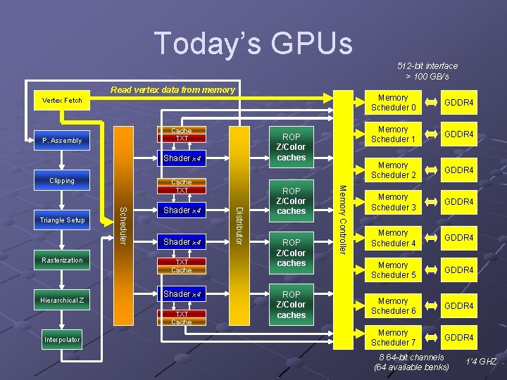
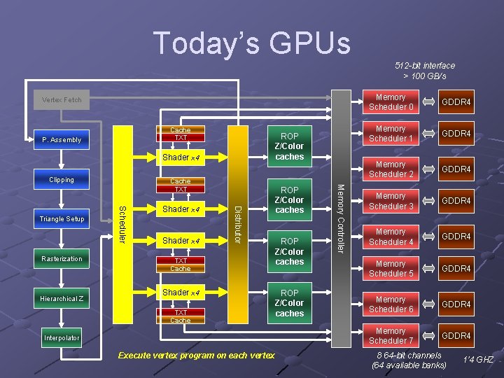
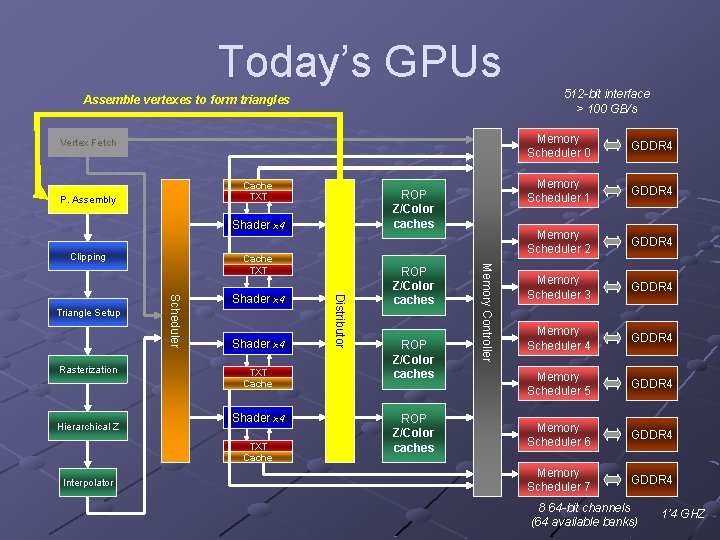
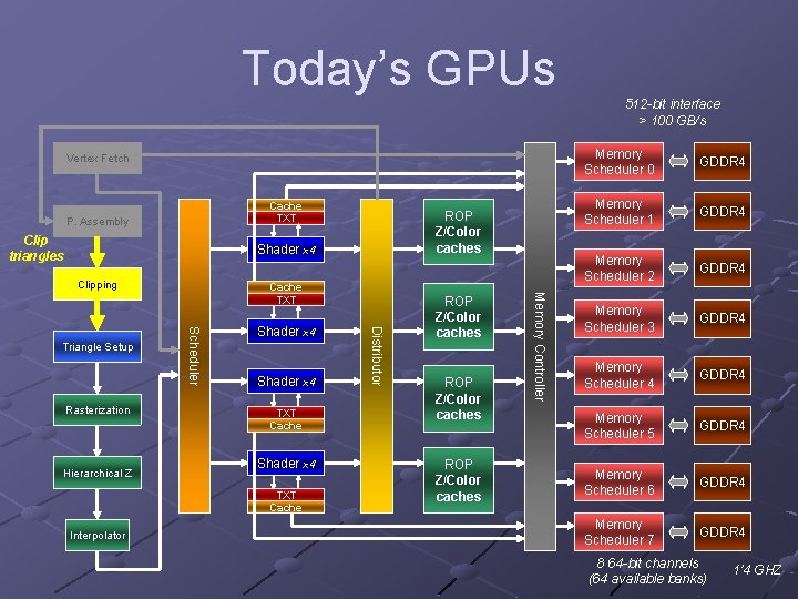
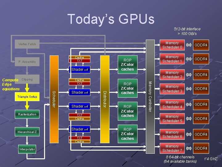
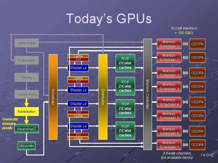
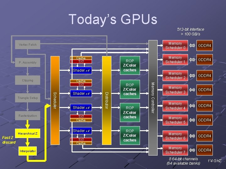
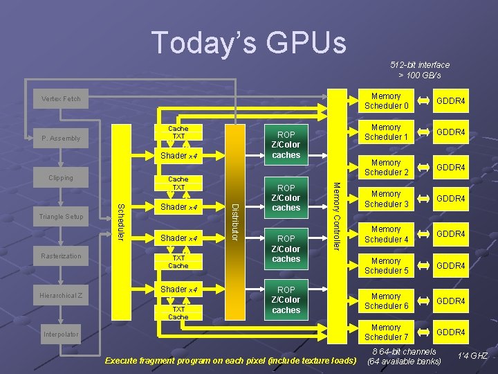
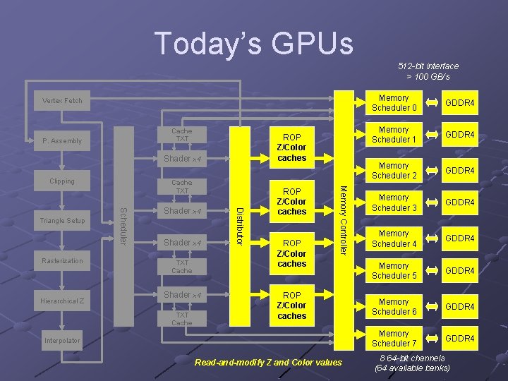
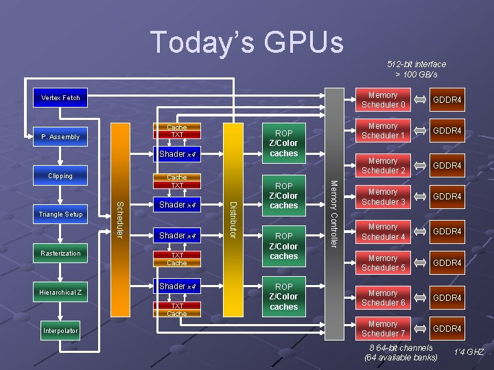
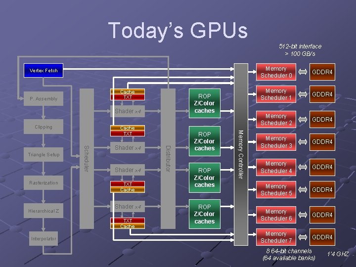
Today’s GPUs Vertex Fetch Cache TXT P. Assembly ROP Z/Color caches Shader x 4 Clipping Shader x 4 TXT Cache Interpolator ROP Z/Color caches Memory Controller Hierarchical Z Shader x 4 Distributor Rasterization Scheduler Triangle Setup Cache TXT 512 -bit interface > 100 GB/s Memory Scheduler 0 GDDR 4 Memory Scheduler 1 GDDR 4 Memory Scheduler 2 GDDR 4 Memory Scheduler 3 GDDR 4 Memory Scheduler 4 GDDR 4 Memory Scheduler 5 GDDR 4 Memory Scheduler 6 GDDR 4 Memory Scheduler 7 GDDR 4 8 64 -bit channels (64 available banks) 1’ 4 GHZ

Today’s GPUs Read vertex data from memory Vertex Fetch Cache TXT P. Assembly ROP Z/Color caches Shader x 4 Clipping Shader x 4 TXT Cache Interpolator ROP Z/Color caches Memory Controller Hierarchical Z Shader x 4 Distributor Rasterization Scheduler Triangle Setup Cache TXT 512 -bit interface > 100 GB/s Memory Scheduler 0 GDDR 4 Memory Scheduler 1 GDDR 4 Memory Scheduler 2 GDDR 4 Memory Scheduler 3 GDDR 4 Memory Scheduler 4 GDDR 4 Memory Scheduler 5 GDDR 4 Memory Scheduler 6 GDDR 4 Memory Scheduler 7 GDDR 4 8 64 -bit channels (64 available banks) 1’ 4 GHZ

Today’s GPUs Vertex Fetch Cache TXT P. Assembly ROP Z/Color caches Shader x 4 Clipping Shader x 4 TXT Cache Interpolator Execute vertex program on each vertex ROP Z/Color caches Memory Controller Hierarchical Z Shader x 4 Distributor Rasterization Scheduler Triangle Setup Cache TXT 512 -bit interface > 100 GB/s Memory Scheduler 0 GDDR 4 Memory Scheduler 1 GDDR 4 Memory Scheduler 2 GDDR 4 Memory Scheduler 3 GDDR 4 Memory Scheduler 4 GDDR 4 Memory Scheduler 5 GDDR 4 Memory Scheduler 6 GDDR 4 Memory Scheduler 7 GDDR 4 8 64 -bit channels (64 available banks) 1’ 4 GHZ

Today’s GPUs Assemble vertexes to form triangles Vertex Fetch Cache TXT P. Assembly ROP Z/Color caches Shader x 4 Clipping Shader x 4 TXT Cache Interpolator ROP Z/Color caches Memory Controller Hierarchical Z Shader x 4 Distributor Rasterization Scheduler Triangle Setup Cache TXT 512 -bit interface > 100 GB/s Memory Scheduler 0 GDDR 4 Memory Scheduler 1 GDDR 4 Memory Scheduler 2 GDDR 4 Memory Scheduler 3 GDDR 4 Memory Scheduler 4 GDDR 4 Memory Scheduler 5 GDDR 4 Memory Scheduler 6 GDDR 4 Memory Scheduler 7 GDDR 4 8 64 -bit channels (64 available banks) 1’ 4 GHZ

Today’s GPUs Vertex Fetch Cache TXT P. Assembly Clip triangles ROP Z/Color caches Shader x 4 Clipping Shader x 4 TXT Cache Interpolator ROP Z/Color caches Memory Controller Hierarchical Z Shader x 4 Distributor Rasterization Scheduler Triangle Setup Cache TXT 512 -bit interface > 100 GB/s Memory Scheduler 0 GDDR 4 Memory Scheduler 1 GDDR 4 Memory Scheduler 2 GDDR 4 Memory Scheduler 3 GDDR 4 Memory Scheduler 4 GDDR 4 Memory Scheduler 5 GDDR 4 Memory Scheduler 6 GDDR 4 Memory Scheduler 7 GDDR 4 8 64 -bit channels (64 available banks) 1’ 4 GHZ

Today’s GPUs Vertex Fetch Cache TXT P. Assembly ROP Z/Color caches Shader x 4 Hierarchical Z Shader x 4 TXT Cache Interpolator ROP Z/Color caches Memory Controller Rasterization Scheduler Triangle Setup Cache TXT Distributor Compute Edge equations Clipping 512 -bit interface > 100 GB/s Memory Scheduler 0 GDDR 4 Memory Scheduler 1 GDDR 4 Memory Scheduler 2 GDDR 4 Memory Scheduler 3 GDDR 4 Memory Scheduler 4 GDDR 4 Memory Scheduler 5 GDDR 4 Memory Scheduler 6 GDDR 4 Memory Scheduler 7 GDDR 4 8 64 -bit channels (64 available banks) 1’ 4 GHZ

Today’s GPUs Vertex Fetch Cache TXT P. Assembly ROP Z/Color caches Shader x 4 Clipping Shader x 4 TXT Cache Interpolator ROP Z/Color caches Memory Controller Generate triangle pixels Hierarchical Z Shader x 4 Distributor Rasterization Scheduler Triangle Setup Cache TXT 512 -bit interface > 100 GB/s Memory Scheduler 0 GDDR 4 Memory Scheduler 1 GDDR 4 Memory Scheduler 2 GDDR 4 Memory Scheduler 3 GDDR 4 Memory Scheduler 4 GDDR 4 Memory Scheduler 5 GDDR 4 Memory Scheduler 6 GDDR 4 Memory Scheduler 7 GDDR 4 8 64 -bit channels (64 available banks) 1’ 4 GHZ

Today’s GPUs Vertex Fetch Cache TXT P. Assembly ROP Z/Color caches Shader x 4 Clipping Fast Z discard Shader x 4 TXT Cache Interpolator ROP Z/Color caches Memory Controller Hierarchical Z Shader x 4 Distributor Rasterization Scheduler Triangle Setup Cache TXT 512 -bit interface > 100 GB/s Memory Scheduler 0 GDDR 4 Memory Scheduler 1 GDDR 4 Memory Scheduler 2 GDDR 4 Memory Scheduler 3 GDDR 4 Memory Scheduler 4 GDDR 4 Memory Scheduler 5 GDDR 4 Memory Scheduler 6 GDDR 4 Memory Scheduler 7 GDDR 4 8 64 -bit channels (64 available banks) 1’ 4 GHZ

Today’s GPUs Vertex Fetch Cache TXT P. Assembly ROP Z/Color caches Shader x 4 Clipping Shader x 4 TXT Cache ROP Z/Color caches Memory Controller Hierarchical Z Shader x 4 Distributor Rasterization Scheduler Triangle Setup Cache TXT ROP Z/Color caches Interpolator Execute fragment program on each pixel (include texture loads) 512 -bit interface > 100 GB/s Memory Scheduler 0 GDDR 4 Memory Scheduler 1 GDDR 4 Memory Scheduler 2 GDDR 4 Memory Scheduler 3 GDDR 4 Memory Scheduler 4 GDDR 4 Memory Scheduler 5 GDDR 4 Memory Scheduler 6 GDDR 4 Memory Scheduler 7 GDDR 4 8 64 -bit channels (64 available banks) 1’ 4 GHZ

Today’s GPUs Vertex Fetch Cache TXT P. Assembly ROP Z/Color caches Shader x 4 Clipping Shader x 4 TXT Cache ROP Z/Color caches Memory Controller Hierarchical Z Shader x 4 Distributor Rasterization Scheduler Triangle Setup Cache TXT ROP Z/Color caches Interpolator Read-and-modify Z and Color values 512 -bit interface > 100 GB/s Memory Scheduler 0 GDDR 4 Memory Scheduler 1 GDDR 4 Memory Scheduler 2 GDDR 4 Memory Scheduler 3 GDDR 4 Memory Scheduler 4 GDDR 4 Memory Scheduler 5 GDDR 4 Memory Scheduler 6 GDDR 4 Memory Scheduler 7 GDDR 4 8 64 -bit channels (64 available banks)

Today’s GPUs Vertex Fetch Cache TXT P. Assembly ROP Z/Color caches Shader x 4 Clipping Shader x 4 TXT Cache Interpolator ROP Z/Color caches Memory Controller Hierarchical Z Shader x 4 Distributor Rasterization Scheduler Triangle Setup Cache TXT 512 -bit interface > 100 GB/s Memory Scheduler 0 GDDR 4 Memory Scheduler 1 GDDR 4 Memory Scheduler 2 GDDR 4 Memory Scheduler 3 GDDR 4 Memory Scheduler 4 GDDR 4 Memory Scheduler 5 GDDR 4 Memory Scheduler 6 GDDR 4 Memory Scheduler 7 GDDR 4 8 64 -bit channels (64 available banks) 1’ 4 GHZ

Today’s GPUs Vertex Fetch Cache TXT P. Assembly ROP Z/Color caches Shader x 4 Clipping Shader x 4 TXT Cache Interpolator ROP Z/Color caches Memory Controller Hierarchical Z Shader x 4 Distributor Rasterization Scheduler Triangle Setup Cache TXT 512 -bit interface > 100 GB/s Memory Scheduler 0 GDDR 4 Memory Scheduler 1 GDDR 4 Memory Scheduler 2 GDDR 4 Memory Scheduler 3 GDDR 4 Memory Scheduler 4 GDDR 4 Memory Scheduler 5 GDDR 4 Memory Scheduler 6 GDDR 4 Memory Scheduler 7 GDDR 4 8 64 -bit channels (64 available banks) 1’ 4 GHZ

Today’s GPUs remarks Tremendous bandwidth available but… Dozens of clients can access memory simultaneously Unbalance and inneficient scheduling of memory transactions can lead to poor performance n Workload unbalance Less total available BW n Inneficient scheduling Latency increases (DDR protocol overhead) Overall performance degradation

Contents Today’s GPUs Thesis Goals Methodology Publications Thesis current state Conclusions

Thesis Goals Propose new cache hierarchies for ROP and texture units. Optimize bank mapping and load balancing among memory channels. Also, propose multiple separated address spaces. Propose an efficient memory controller scheduler. Research in interconnection topologies. Measure power consumption of our proposals.

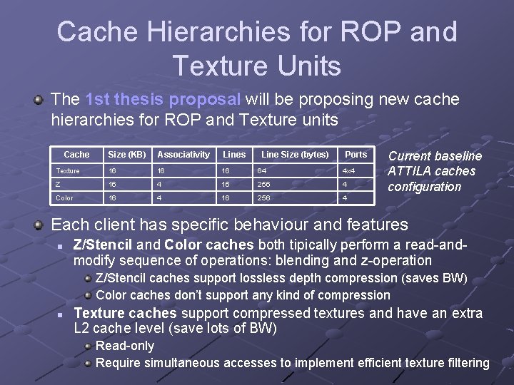
Cache Hierarchies for ROP and Texture Units The 1 st thesis proposal will be proposing new cache hierarchies for ROP and Texture units Cache Size (KB) Associativity Lines Line Size (bytes) Ports Texture 16 16 16 64 4 x 4 Z 16 4 16 256 4 Color 16 4 16 256 4 Current baseline ATTILA caches configuration Each client has specific behaviour and features n Z/Stencil and Color caches both tipically perform a read-andmodify sequence of operations: blending and z-operation Z/Stencil caches support lossless depth compression (saves BW) Color caches don’t support any kind of compression n Texture caches support compressed textures and have an extra L 2 cache level (save lots of BW) Read-only Require simultaneous accesses to implement efficient texture filtering

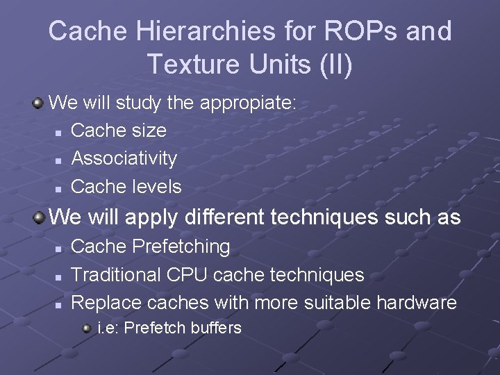
Cache Hierarchies for ROPs and Texture Units (II) We will study the appropiate: n Cache size n Associativity n Cache levels We will apply different techniques such as n n n Cache Prefetching Traditional CPU cache techniques Replace caches with more suitable hardware i. e: Prefetch buffers

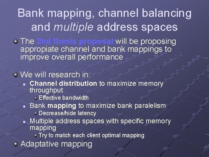
Bank mapping, channel balancing and multiple address spaces The 2 nd thesis proposal will be proposing appropiate channel and bank mappings to improve overall performance We will research in: n Channel distribution to maximize memory throughput Effective bandwidth n Bank mapping to maximize bank paralelism Decrease/hide latency n Multiple address spaces with specific memory mapping Try to match each client optimal mapping Adaptative mapping

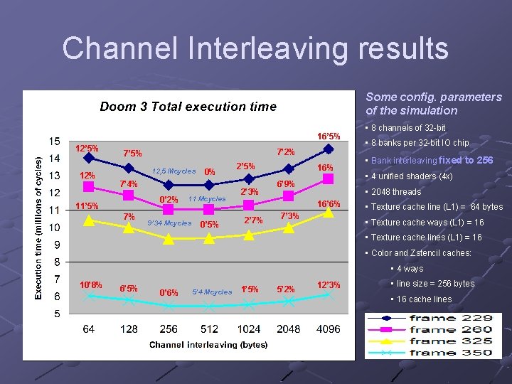
Channel Interleaving results Some config. parameters of the simulation 16’ 5% 12% 7’ 5% 12, 5 Mcycles 0% 7’ 4% 0’ 2% 11’ 5% 7% 11 Mcycles 9’ 34 Mcycles 0’ 5% 2’ 3% 16% 6’ 9% • 8 banks per 32 -bit IO chip • Bank interleaving fixed to 256 • 4 unified shaders (4 x) • 2048 threads 16’ 6% 2’ 7% • 8 channels of 32 -bit 7’ 3% • Texture cache line (L 1) = 64 bytes • Texture cache ways (L 1) = 16 • Texture cache lines (L 1) = 16 • Color and Zstencil caches: • 4 ways 10’ 8% 6’ 5% 0’ 6% 5’ 4 Mcycles 1’ 5% 5’ 2% 12’ 3% • line size = 256 bytes • 16 cache lines

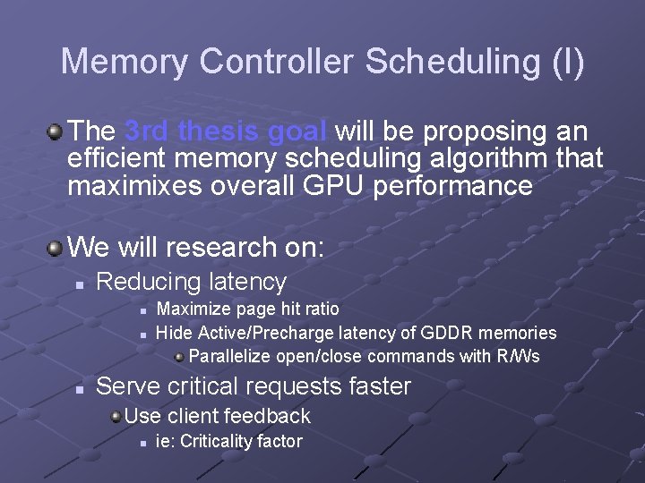
Memory Controller Scheduling (I) The 3 rd thesis goal will be proposing an efficient memory scheduling algorithm that maximixes overall GPU performance We will research on: n Reducing latency n n n Maximize page hit ratio Hide Active/Precharge latency of GDDR memories Parallelize open/close commands with R/Ws Serve critical requests faster Use client feedback n ie: Criticality factor

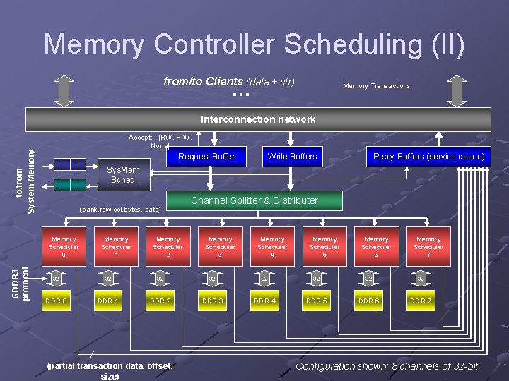
Memory Controller Scheduling (II) from/to Clients (data + ctr) … Memory Transactions Interconnection network to/from System Memory Accept: : {RW, R, W, None} Request Buffer Reply Buffers (service queue) Sys. Mem Sched. (bank, row, col, bytes, data) Memory Scheduler 0 GDDR 3 protocol Write Buffers Memory Scheduler 1 Memory Scheduler 2 Channel Splitter & Distributer Memory Scheduler 3 Memory Scheduler 4 Memory Scheduler 5 Memory Scheduler 6 Memory Scheduler 7 32 32 DDR 0 DDR 1 DDR 2 DDR 3 DDR 4 DDR 5 DDR 6 DDR 7 (partial transaction data, offset, size) Configuration shown: 8 channels of 32 -bit

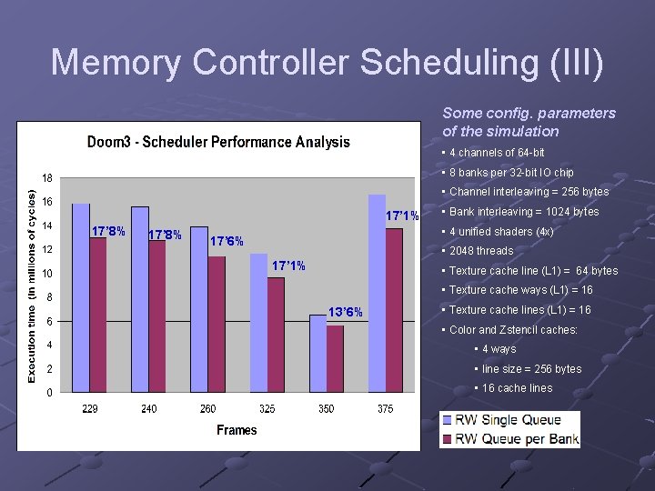
Memory Controller Scheduling (III) Some config. parameters of the simulation • 4 channels of 64 -bit • 8 banks per 32 -bit IO chip • Channel interleaving = 256 bytes 17’ 1% 17’ 8% • Bank interleaving = 1024 bytes • 4 unified shaders (4 x) 17’ 6% • 2048 threads 17’ 1% • Texture cache line (L 1) = 64 bytes • Texture cache ways (L 1) = 16 13’ 6% • Texture cache lines (L 1) = 16 • Color and Zstencil caches: • 4 ways • line size = 256 bytes • 16 cache lines

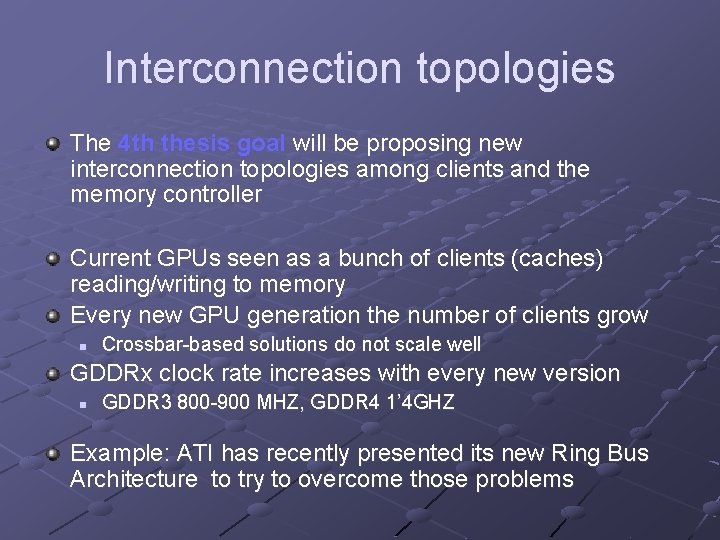
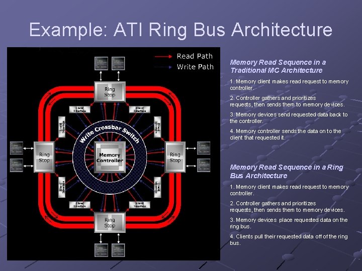
Interconnection topologies The 4 th thesis goal will be proposing new interconnection topologies among clients and the memory controller Current GPUs seen as a bunch of clients (caches) reading/writing to memory Every new GPU generation the number of clients grow n Crossbar-based solutions do not scale well GDDRx clock rate increases with every new version n GDDR 3 800 -900 MHZ, GDDR 4 1’ 4 GHZ Example: ATI has recently presented its new Ring Bus Architecture to try to overcome those problems

Example: ATI Ring Bus Architecture Memory Read Sequence in a Traditional MC Architecture 1. Memory client makes read request to memory controller. 2. Controller gathers and prioritizes requests, then sends them to memory devices. 3. Memory devices send requested data back to the controller. 4. Memory controller sends the data on to the client that requested it. Memory Read Sequence in a Ring Bus Architecture 1. Memory client makes read request to memory controller. 2. Controller gathers and prioritizes requests, then sends them to memory devices. 3. Memory devices place requested data on the ring bus. 4. Clients pull their requested data off of the ring bus.

Power Evaluation Our last thesis goal will be evaluating the power consumption of our proposals Power model based on: n Calculating Memory System Power for DDR 3 SDRAM, Micron Designline, April 2007. Evaluates only DRAM consumption This evaluation allows to compute power based on DDR 3 commands and current state of the dram chips (open pages, etc). n ATTILA inherent cycle-to-cycle and highly detailed simulation has all required information to implement this model

Contents Today’s GPUs Thesis Goals Methodology Publications Thesis current state Conclusions

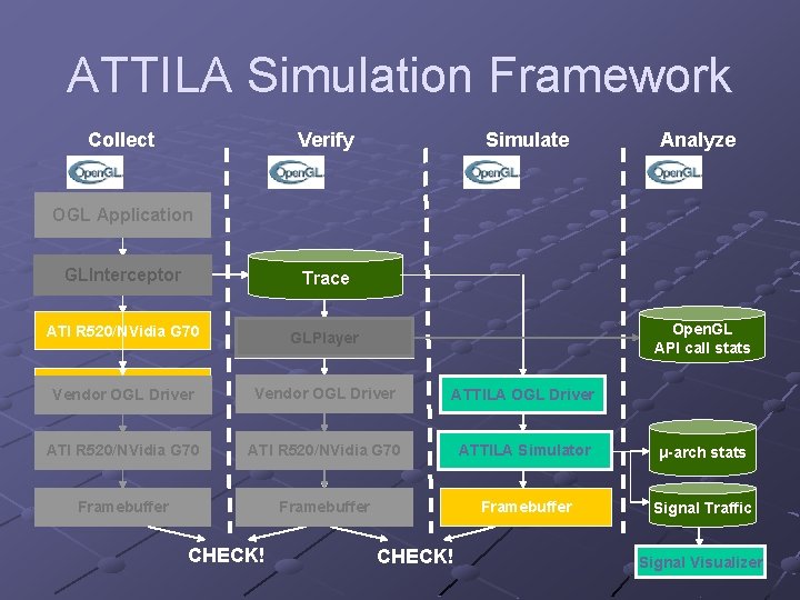
ATTILA Simulation Framework Collect Verify Simulate Analyze OGL Application Vendor OGL Driver GLInterceptor Trace ATI R 520/NVidia G 70 GLPlayer Framebuffer Vendor OGL Driver ATTILA OGL Driver ATI R 520/NVidia G 70 ATTILA Simulator μ-arch stats Framebuffer Signal Traffic CHECK! Open. GL API call stats CHECK! Signal Visualizer

Contents Today’s GPUs Thesis Goals Methodology Publications Thesis current state Conclusions

ATTILA Group Publications Victor Moya, Carlos Gonzalez, Jordi Roca, et al. Shader Performance Analysis on a Modern GPU Architecture. Micro 38, 2005. Victor Moya, Carlos Gonzalez, Jordi Roca, et al. A Single (Unified) Shader GPU Microarchitecture for Embedded Systems. Hi- PEAC 2005. V. Moya, Carlos Gonzalez, Jordi Rocat, et al. ATTILA: A Cycle. Level. Execution-Driven Simulator for Modern GPU Architectures. IEEE International Symposium on Performance Analysis of Systems and Software (ISPASS-2006) March 19 -21, 2006, Austin, Texas. J. Roca, V. Moya, Carlos Gonzalez, et al. Workload Characterization of 3 D Games. IEEE International Symposium on Workload Characterization (IISWC-2006) October 25 -27, 2006, San Jose, California.

Contents Today’s GPUs Thesis Goals Methodology Publications Thesis current state Conclusions

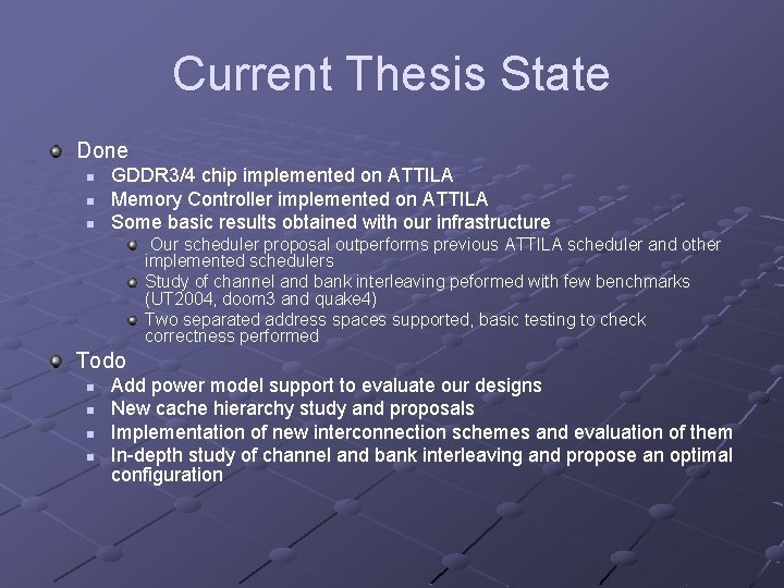
Current Thesis State Done n n n GDDR 3/4 chip implemented on ATTILA Memory Controller implemented on ATTILA Some basic results obtained with our infrastructure Our scheduler proposal outperforms previous ATTILA scheduler and other implemented schedulers Study of channel and bank interleaving peformed with few benchmarks (UT 2004, doom 3 and quake 4) Two separated address spaces supported, basic testing to check correctness performed Todo n n Add power model support to evaluate our designs New cache hierarchy study and proposals Implementation of new interconnection schemes and evaluation of them In-depth study of channel and bank interleaving and propose an optimal configuration

Contents Today’s GPUs Thesis Goals Methodology Publications Thesis current state Conclusions

Conclusions GPU memory system is crucial and can be a bottleneck, to attack this problem we propose: n n n New caches hierarchies for ROPs and Texture units clients Improving channel and bank mapping to optimize the memory throughput Optimize the memory transaction scheduling Research on new memory controller interconnection with clients Evaluate power consumption of our proposals

GPU Memory Hierarchy Optimizations Carlos González Rodríguez Advisors: Roger Espasa and Agustín Fernández Departament d’Arquitectura de Computadors (DAC) Universitat Politècnica de Catalunya (UPC) June 2007