Recap Memory Hierarchy 1 Memory Hierarchy the Big

Recap: Memory Hierarchy 1
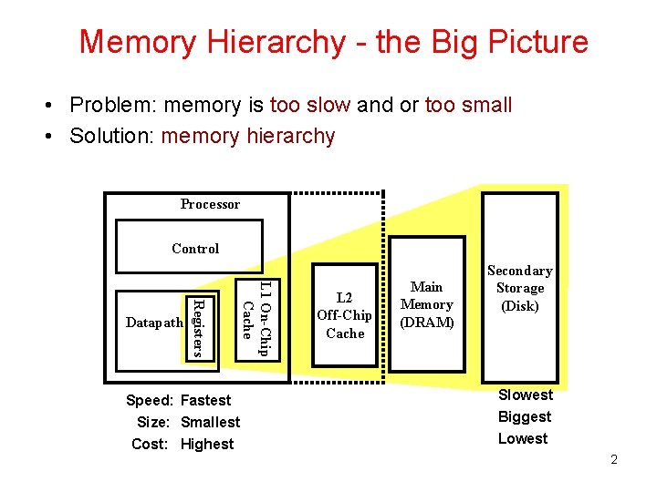
Memory Hierarchy - the Big Picture • Problem: memory is too slow and or too small • Solution: memory hierarchy Processor Control L 1 On-Chip Cache Registers Datapath Speed: Fastest Size: Smallest Cost: Highest L 2 Off-Chip Cache Main Memory (DRAM) Secondary Storage (Disk) Slowest Biggest Lowest 2
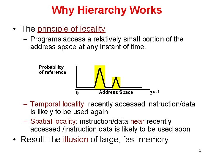
Why Hierarchy Works • The principle of locality – Programs access a relatively small portion of the address space at any instant of time. Probability of reference 0 Address Space 2 n - 1 – Temporal locality: recently accessed instruction/data is likely to be used again – Spatial locality: instruction/data near recently accessed /instruction data is likely to be used soon • Result: the illusion of large, fast memory 3
![Example of Locality int A[100], B[100], C[100], D; for (i=0; i<100; i++) { C[i] Example of Locality int A[100], B[100], C[100], D; for (i=0; i<100; i++) { C[i]](http://slidetodoc.com/presentation_image_h2/6824a30a947a7d6937f6eccb3b817b42/image-4.jpg)
Example of Locality int A[100], B[100], C[100], D; for (i=0; i<100; i++) { C[i] = A[i] * B[i] + D; } D C[99] C[98] C[97] C[96] . . . C[7] C[6] C[5] C[4] C[3] C[2] C[1] C[0] . . . B[11] B[10] B[3] B[2] B[9] B[1] B[8] B[0] B[7] B[6] B[5] B[4] A[99] A[98] A[97] A[96] . . . A[7] A[6] A[5] A[4] A[3] A[2] A[1] A[0] 4
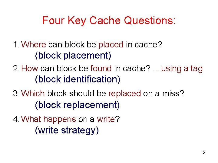
Four Key Cache Questions: 1. Where can block be placed in cache? (block placement) 2. How can block be found in cache? …using a tag (block identification) 3. Which block should be replaced on a miss? (block replacement) 4. What happens on a write? (write strategy) 5
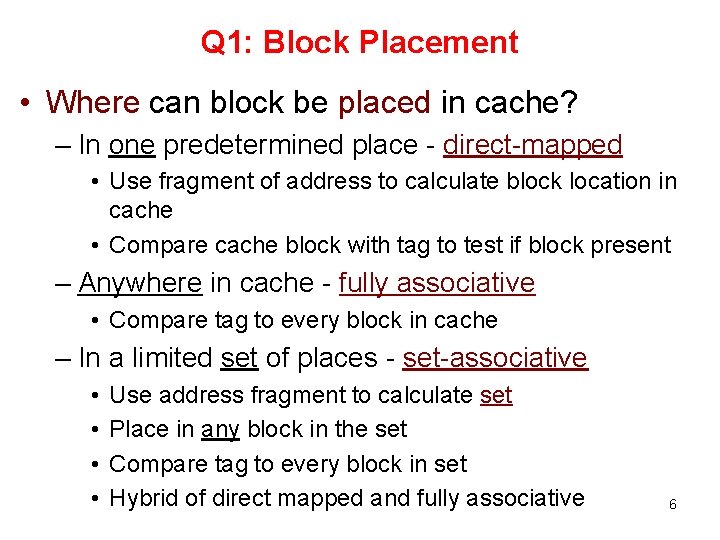
Q 1: Block Placement • Where can block be placed in cache? – In one predetermined place - direct-mapped • Use fragment of address to calculate block location in cache • Compare cache block with tag to test if block present – Anywhere in cache - fully associative • Compare tag to every block in cache – In a limited set of places - set-associative • • Use address fragment to calculate set Place in any block in the set Compare tag to every block in set Hybrid of direct mapped and fully associative 6
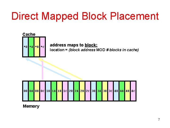
Direct Mapped Block Placement Cache *0 *4 *8 *C address maps to block: location = (block address MOD # blocks in cache) 00 04 08 0 C 10 14 18 1 C 20 24 28 2 C 30 34 38 3 C 40 44 48 4 C Memory 7
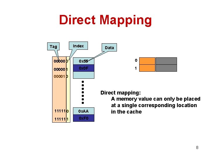
Direct Mapping Tag Index Data 00000 0 0 x 55 0 00000 1 0 x 0 F 1 00001 0 11111 0 0 x. AA 11111 1 0 x. F 0 Direct mapping: A memory value can only be placed at a single corresponding location in the cache 8
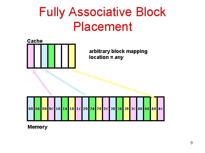
Fully Associative Block Placement Cache arbitrary block mapping location = any 00 04 08 0 C 10 14 18 1 C 20 24 28 2 C 30 34 38 3 C 40 44 48 4 C Memory 9
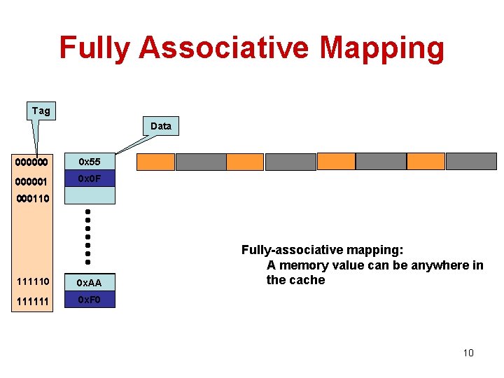
Fully Associative Mapping Tag Data 000000 0 x 55 000001 0000 0 x 0 F 000110 111110 0 x. AA 111111 0 x. F 0 Fully-associative mapping: A memory value can be anywhere in the cache 10
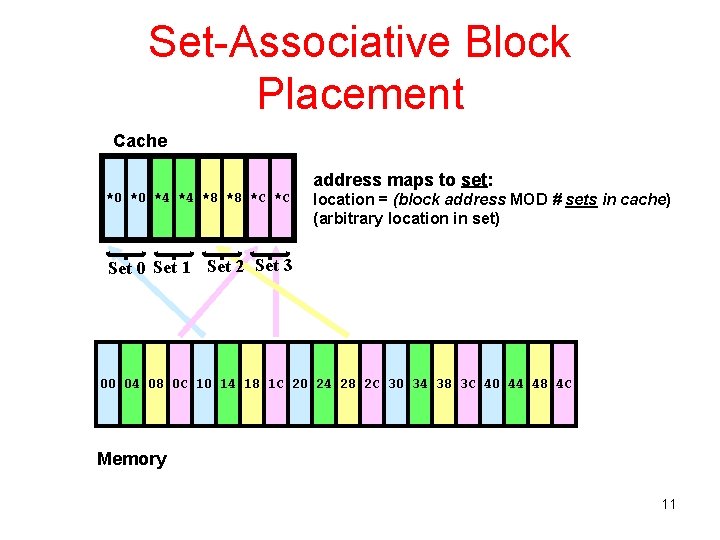
Set-Associative Block Placement Cache address maps to set: *0 *0 *4 *4 *8 *8 *C *C location = (block address MOD # sets in cache) (arbitrary location in set) Set 0 Set 1 Set 2 Set 3 00 04 08 0 C 10 14 18 1 C 20 24 28 2 C 30 34 38 3 C 40 44 48 4 C Memory 11
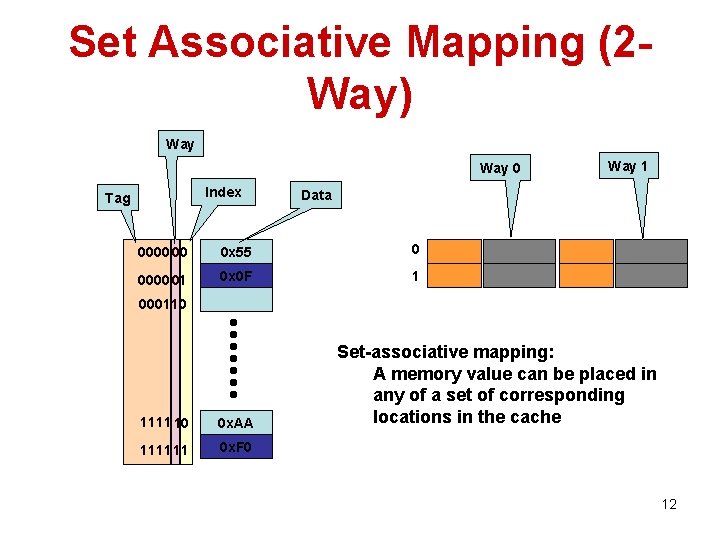
Set Associative Mapping (2 Way) Way 0 Index Tag Way 1 Data 0000 00 0 x 55 0 0000 01 0 x 0 F 1 0001 10 1111 10 0 x. AA 1111 11 0 x. F 0 Set-associative mapping: A memory value can be placed in any of a set of corresponding locations in the cache 12
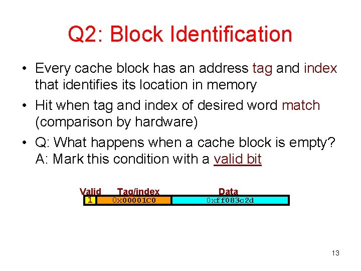
Q 2: Block Identification • Every cache block has an address tag and index that identifies its location in memory • Hit when tag and index of desired word match (comparison by hardware) • Q: What happens when a cache block is empty? A: Mark this condition with a valid bit Valid 1 Tag/index 0 x 00001 C 0 Data 0 xff 083 c 2 d 13
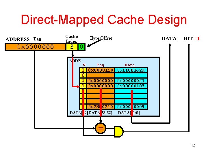
Direct-Mapped Cache Design ADDRESS Tag 0 x 0000000 Cache Index DATA Byte Offset HIT =1 3 0 ADDR V 1 0 1 1 0 0 1 0 Tag Data 0 x 00001 C 0 0 xff 083 c 2 d 0 x 0000000 0 x 00000021 0 x 0000000 0 x 00000103 CACHE SRAM 0 x 23 F 0210 0 x 00000009 DATA[59] DATA[58: 32] DATA[31: 0] = 14
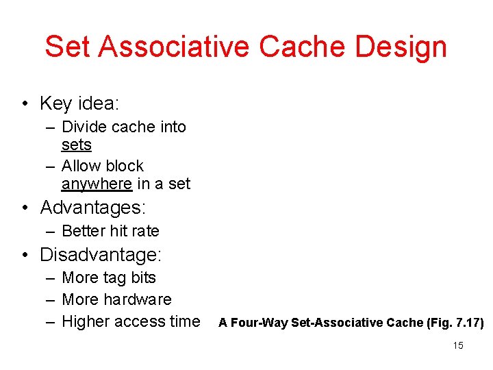
Set Associative Cache Design • Key idea: – Divide cache into sets – Allow block anywhere in a set • Advantages: – Better hit rate • Disadvantage: – More tag bits – More hardware – Higher access time A Four-Way Set-Associative Cache (Fig. 7. 17) 15
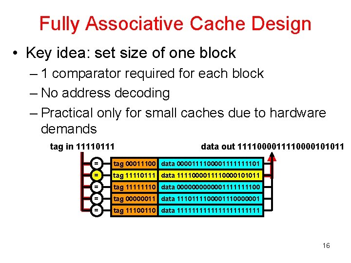
Fully Associative Cache Design • Key idea: set size of one block – 1 comparator required for each block – No address decoding – Practical only for small caches due to hardware demands tag in 11110111 data out 11110000101011 = tag 00011100 data 00001111111101 = tag 11110111 data 11110000101011 = tag 11111110 data 000000111100 = tag 00000011 data 111011110000001 = tag 11100110 data 11111111111 16
Cache Replacement Policy • Random – Replace a randomly chosen line • LRU (Least Recently Used) – Replace the least recently used line 17
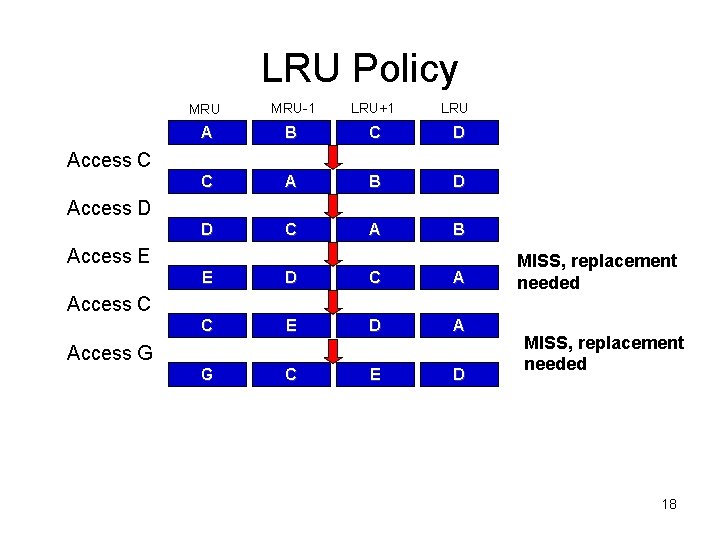
LRU Policy MRU-1 LRU+1 LRU A B C D C A B D D C A B Access C Access D Access E E D C A C E D A G C E D MISS, replacement needed Access C Access G MISS, replacement needed 18
Cache Write Strategies • Need to keep cache consistent with the main memory – Reads are easy - require no modification – Writes- when does the update occur 1 Write Though: Data is written to both the cache block and to a block of main memory. Ø The lower level always has the most updated data; an important feature for I/O and multiprocessing. Ø Easier to implement than write back. 2 Write back: Data is written or updated only to the cache block. The modified or dirty cache block is written to main memory when it’s being replaced from cache. Ø Writes occur at the speed of cache Ø Uses less memory bandwidth than write through. 19
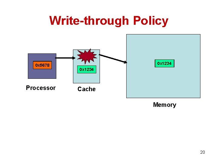
Write-through Policy 0 x 5678 Processor 0 x 1234 Cache Memory 20
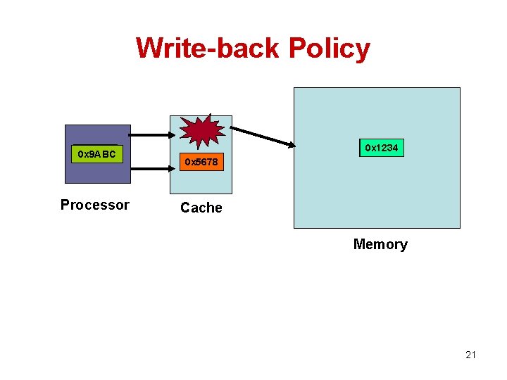
Write-back Policy 0 x 5678 0 x 9 ABC Processor 0 x 1234 0 x 5678 0 x 1234 Cache Memory 21
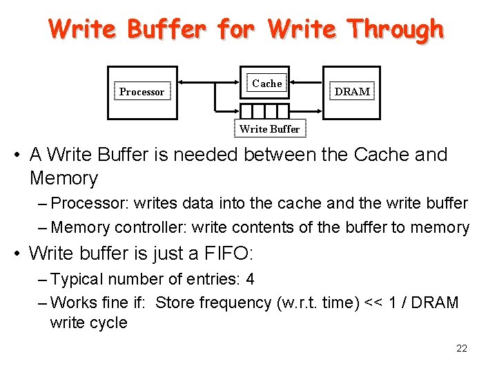
Write Buffer for Write Through Processor Cache DRAM Write Buffer • A Write Buffer is needed between the Cache and Memory – Processor: writes data into the cache and the write buffer – Memory controller: write contents of the buffer to memory • Write buffer is just a FIFO: – Typical number of entries: 4 – Works fine if: Store frequency (w. r. t. time) << 1 / DRAM write cycle 22
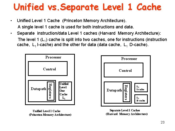
Unified vs. Separate Level 1 Cache • • Unified Level 1 Cache (Princeton Memory Architecture). A single level 1 cache is used for both instructions and data. Separate instruction/data Level 1 caches (Harvard Memory Architecture): The level 1 (L 1) cache is split into two caches, one for instructions (instruction cache, L 1 I-cache) and the other for data (data cache, L 1 D-cache). Processor Control Unified Level One Cache L 1 Unified Level 1 Cache (Princeton Memory Architecture) Datapath Registers Datapath Processor L 1 I-cache L 1 D-cache Separate Level 1 Caches (Harvard Memory Architecture) 23
- Slides: 23