Fundamentals of EMC Grounding John Mc Closkey NASAGSFC



- Slides: 57

Fundamentals of EMC Grounding John Mc. Closkey NASA/GSFC Chief EMC Engineer Code 565 Building 23, room E 203 301 -286 -5498 John. C. Mc. Closkey@nasa. gov 1

Topics l Introduction l Reasons for “Grounding” l “Grounding” in the “Real World” (and in “Real Space”) l Bonding 2

The Ground Mystery “The search for a ‘good ground’ is very similar to the search for the Holy Grail in many respects – tales abound about its existence and we all say we want and need it, but we cannot seem to find it. ” - Warren H. Lewis “Ground is a place where potatoes and carrots thrive. ” - Dr. Bruce Archambeault 3

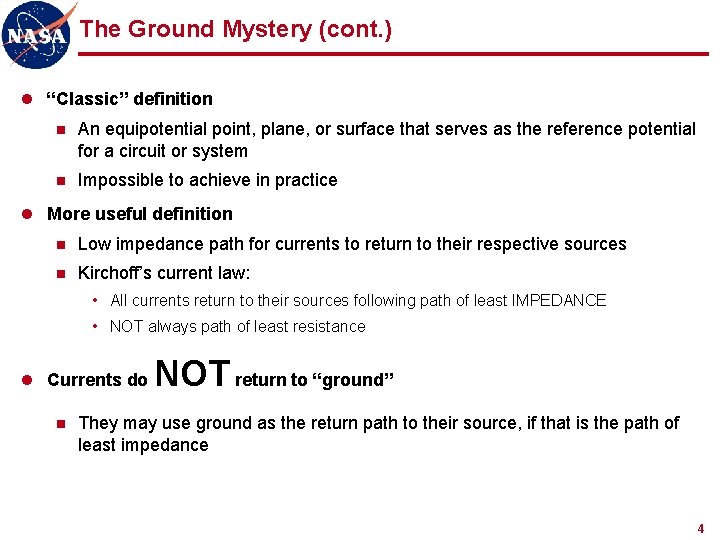
The Ground Mystery (cont. ) l “Classic” definition n An equipotential point, plane, or surface that serves as the reference potential for a circuit or system n Impossible to achieve in practice l More useful definition n Low impedance path for currents to return to their respective sources n Kirchoff’s current law: • All currents return to their sources following path of least IMPEDANCE • NOT always path of least resistance l Currents do n NOT return to “ground” They may use ground as the return path to their source, if that is the path of least impedance 4

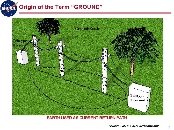
Origin of the Term “GROUND” Ground/Earth Teletype Receiver Teletype Transmitter EARTH USED AS CURRENT RETURN PATH Courtesy of Dr. Bruce Archambeault 5

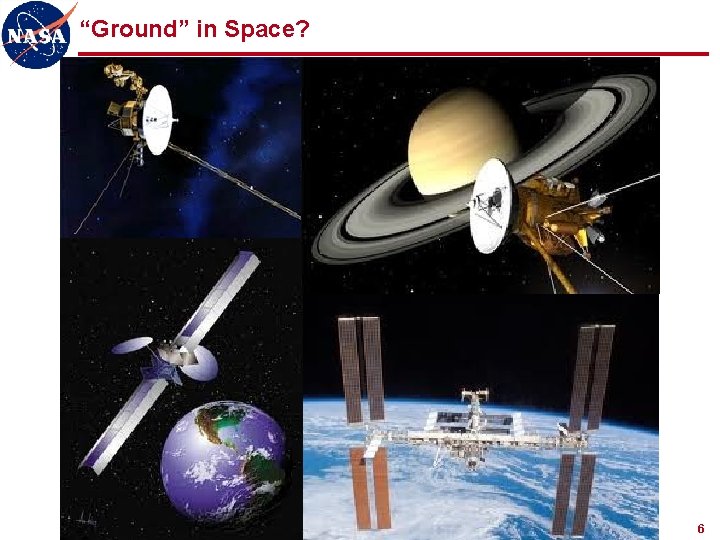
“Ground” in Space? 6

References l Documents available on GSFC EMC Working Group XSPACES page (https: //xspaces. gsfc. nasa. gov/display/EMCWG/Home): n NASA-HDBK-4001, Electrical Grounding Architecture for Unmanned Spacecraft n NASA-HDBK-4002 A, Mitigating In-Space Charging Effects - a Guideline n NASA-STD-4003, Electrical Bonding For NASA Launch Vehicles, Spacecraft, Payloads, and Flight Equipment n NASA-HDBK-419 A, Volumes 1 & 2, Grounding, Bonding, and Shielding for Electronic Equipments And Facilities n IEEE STD 1100™-2005, IEEE Recommended Practice for Powering and Grounding Electronic Equipment (“Emerald Book”) n NASA-HDBK-8739. 21, Workmanship Manual for Electrostatic Discharge Control n Marshall Space Flight Center Electromagnetic Compatibility Design and Interference Control (MEDIC) Handbook n MIL-STD-461 F, Requirements for the Control of Electromagnetic Interference Characteristics of Subsystems and Equipment 7

Topics l Introduction l Reasons for “Grounding” n Safety n Lightning protection n Electrostatic Discharge (ESD) mitigation n Common reference potential n Current return path l “Grounding” in the “Real World” (and in “Real Space”) l Bonding 8

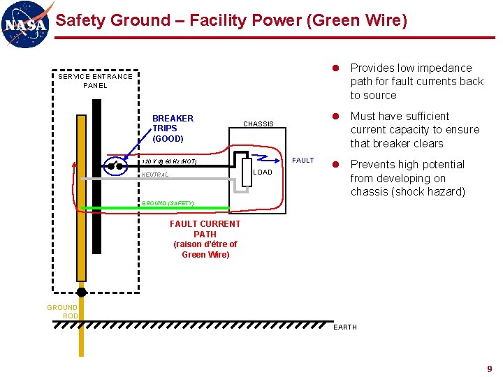
Safety Ground – Facility Power (Green Wire) l Provides low impedance path for fault currents back to source SERVICE ENTRANCE PANEL BREAKER TRIPS (GOOD) FAULT 120 V @ 60 Hz (HOT) LOAD NEUTRAL l Must have sufficient current capacity to ensure that breaker clears CHASSIS l Prevents high potential from developing on chassis (shock hazard) GROUND (SAFETY) FAULT CURRENT PATH (raison d’être of Green Wire) GROUND ROD EARTH 9

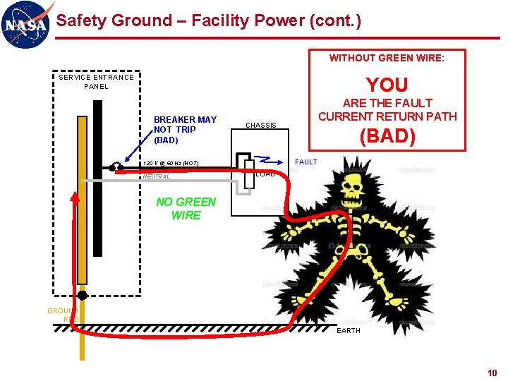
Safety Ground – Facility Power (cont. ) WITHOUT GREEN WIRE: SERVICE ENTRANCE PANEL YOU BREAKER MAY NOT TRIP (BAD) CHASSIS (BAD) FAULT 120 V @ 60 Hz (HOT) NEUTRAL ARE THE FAULT CURRENT RETURN PATH LOAD NO GREEN WIRE GROUND ROD EARTH 10

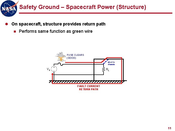
Safety Ground – Spacecraft Power (Structure) l On spacecraft, structure provides return path n Performs same function as green wire FUSE CLEARS (GOOD) short to chassis VS RL FAULT CURRENT RETURN PATH 11

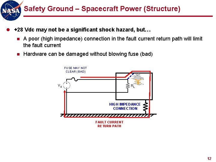
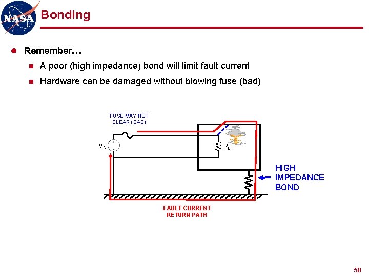
Safety Ground – Spacecraft Power (Structure) l +28 Vdc may not be a significant shock hazard, but… n A poor (high impedance) connection in the fault current return path will limit the fault current n Hardware can be damaged without blowing fuse (bad) FUSE MAY NOT CLEAR (BAD) VS RL HIGH IMPEDANCE CONNECTION FAULT CURRENT RETURN PATH 12

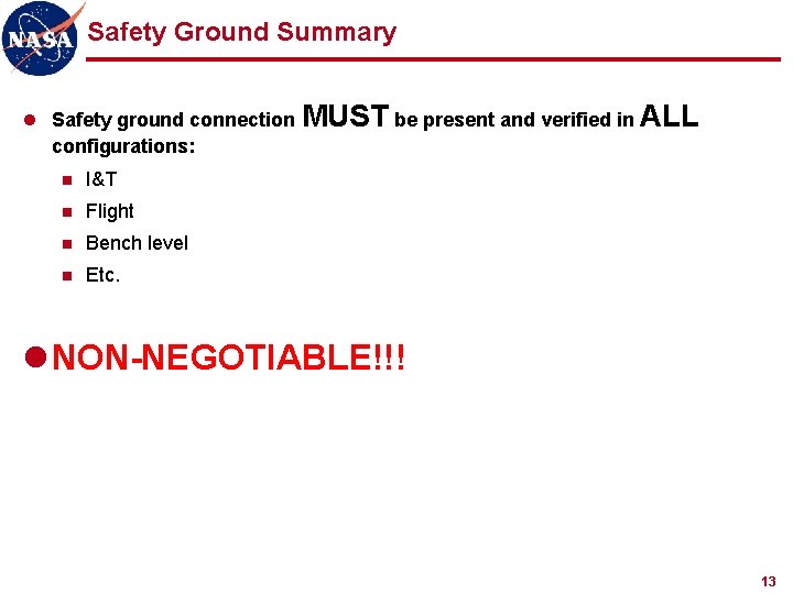
Safety Ground Summary l Safety ground connection MUST be present and verified in ALL configurations: n I&T n Flight n Bench level n Etc. l NON-NEGOTIABLE!!! 13

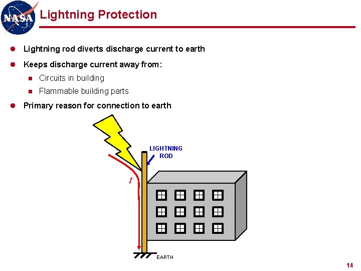
Lightning Protection l Lightning rod diverts discharge current to earth l Keeps discharge current away from: n Circuits in building n Flammable building parts l Primary reason for connection to earth LIGHTNING ROD I EARTH 14

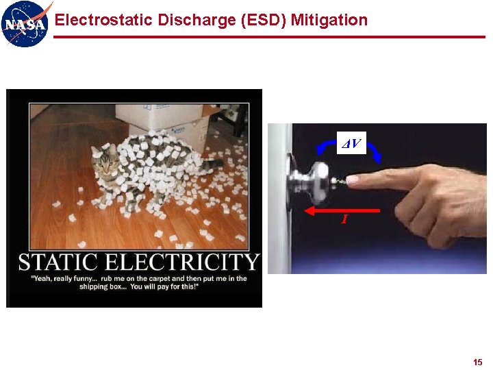
Electrostatic Discharge (ESD) Mitigation ΔV I 15

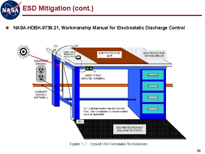
ESD Mitigation (cont. ) l NASA-HDBK-8739. 21, Workmanship Manual for Electrostatic Discharge Control 16

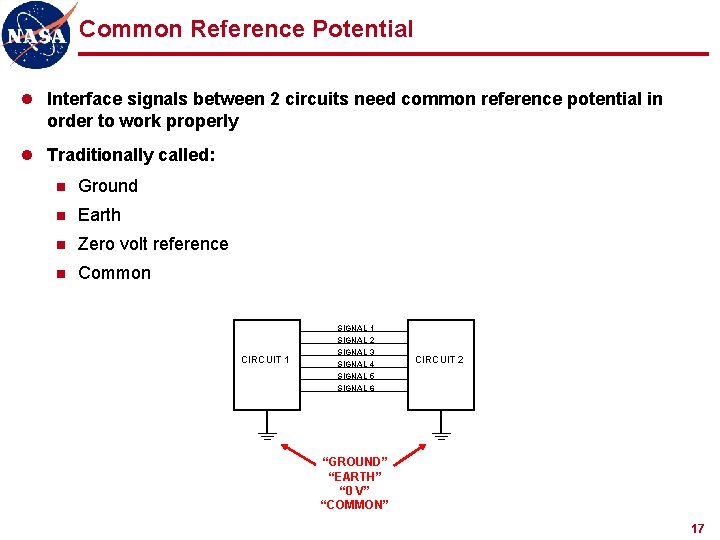
Common Reference Potential l Interface signals between 2 circuits need common reference potential in order to work properly l Traditionally called: n Ground n Earth n Zero volt reference n Common CIRCUIT 1 SIGNAL 2 SIGNAL 3 SIGNAL 4 SIGNAL 5 SIGNAL 6 CIRCUIT 2 “GROUND” “EARTH” “ 0 V” “COMMON” 17

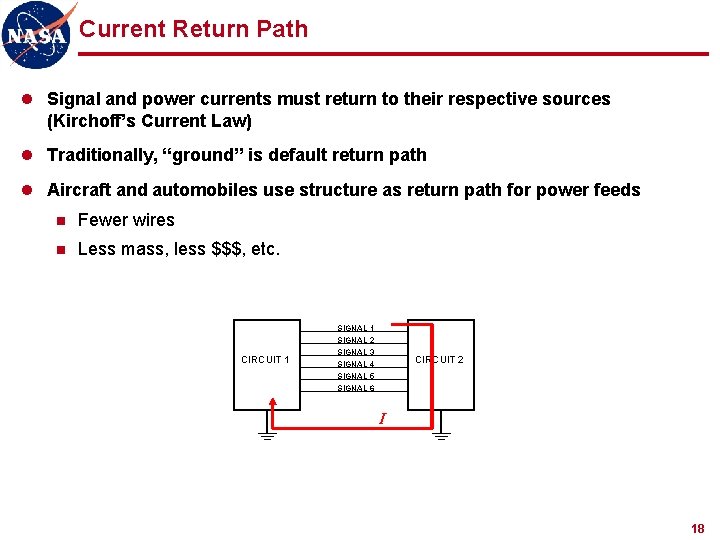
Current Return Path l Signal and power currents must return to their respective sources (Kirchoff’s Current Law) l Traditionally, “ground” is default return path l Aircraft and automobiles use structure as return path for power feeds n Fewer wires n Less mass, less $$$, etc. CIRCUIT 1 SIGNAL 2 SIGNAL 3 SIGNAL 4 SIGNAL 5 SIGNAL 6 CIRCUIT 2 I 18

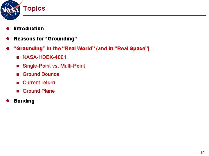
Topics l Introduction l Reasons for “Grounding” l “Grounding” in the “Real World” (and in “Real Space”) n NASA-HDBK-4001 n Single-Point vs. Multi-Point n Ground Bounce n Current return n Ground Plane l Bonding 19

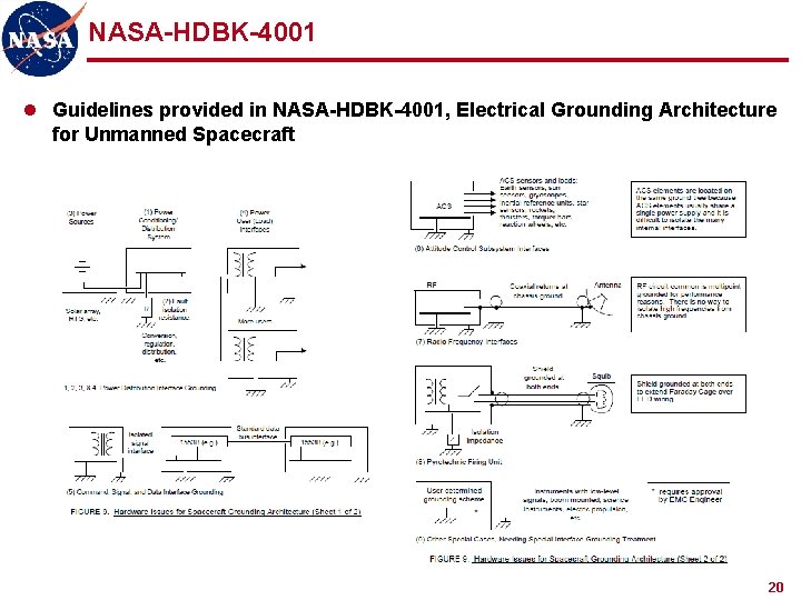
NASA-HDBK-4001 l Guidelines provided in NASA-HDBK-4001, Electrical Grounding Architecture for Unmanned Spacecraft 20

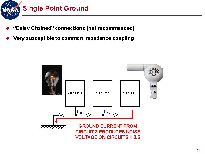
Single Point Ground l “Daisy Chained” connections (not recommended) l Very susceptible to common impedance coupling CIRCUIT 1 VN 1 CIRCUIT 2 CIRCUIT 3 VN 2 GROUND CURRENT FROM CIRCUIT 3 PRODUCES NOISE VOLTAGE ON CIRCUITS 1 & 2 21

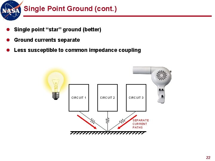
Single Point Ground (cont. ) l Single point “star” ground (better) l Ground currents separate l Less susceptible to common impedance coupling CIRCUIT 1 CIRCUIT 2 CIRCUIT 3 SEPARATE CURRENT PATHS 22

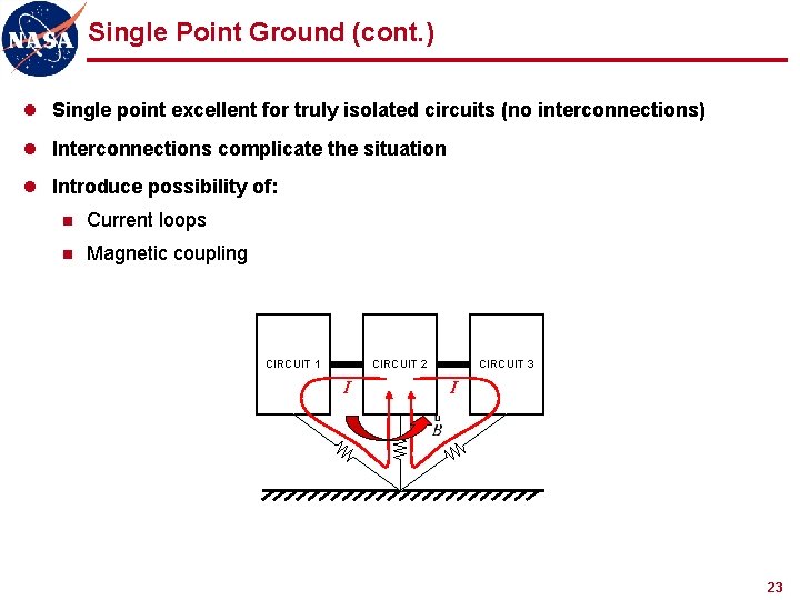
Single Point Ground (cont. ) l Single point excellent for truly isolated circuits (no interconnections) l Interconnections complicate the situation l Introduce possibility of: n Current loops n Magnetic coupling CIRCUIT 1 CIRCUIT 2 I CIRCUIT 3 I 23

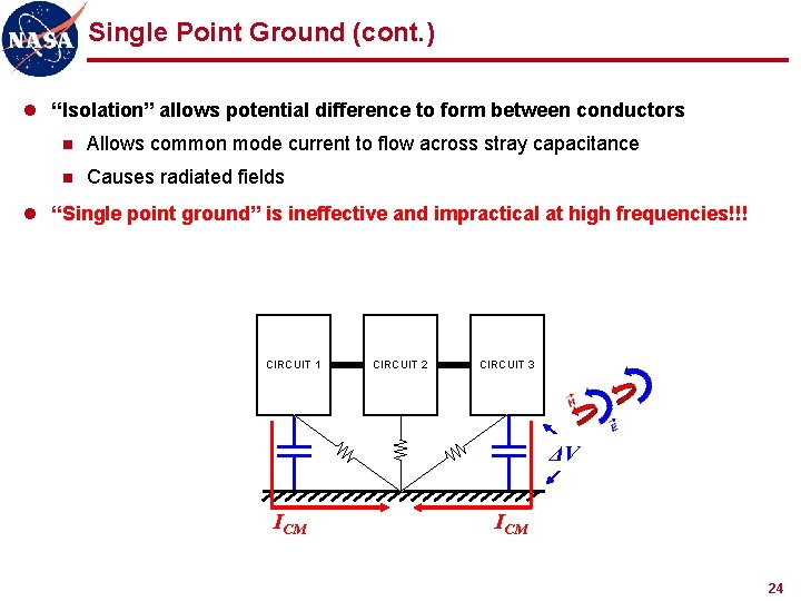
Single Point Ground (cont. ) l “Isolation” allows potential difference to form between conductors n Allows common mode current to flow across stray capacitance n Causes radiated fields l “Single point ground” is ineffective and impractical at high frequencies!!! CIRCUIT 1 CIRCUIT 2 CIRCUIT 3 ΔV ICM 24

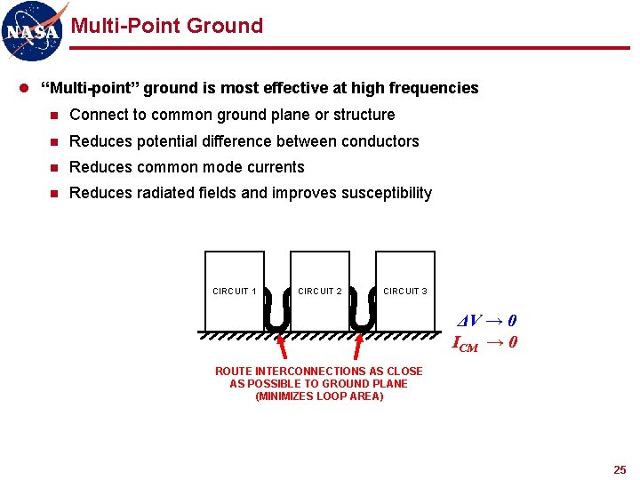
Multi-Point Ground l “Multi-point” ground is most effective at high frequencies n Connect to common ground plane or structure n Reduces potential difference between conductors n Reduces common mode currents n Reduces radiated fields and improves susceptibility CIRCUIT 1 CIRCUIT 2 CIRCUIT 3 ΔV → 0 ICM → 0 ROUTE INTERCONNECTIONS AS CLOSE AS POSSIBLE TO GROUND PLANE (MINIMIZES LOOP AREA) 25

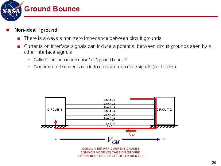
Ground Bounce l Non-ideal “ground” n There is always a non-zero impedance between circuit grounds n Currents on interface signals can induce a potential between circuit grounds seen by all other interface signals • Called “common mode noise” or “ground bounce” • Common mode currents can induce noise on interface signals (next slides) CIRCUIT 1 SIGNAL 2 SIGNAL 3 SIGNAL 4 SIGNAL 5 SIGNAL 6 CIRCUIT 2 Zg - VCM ICM + SIGNAL 1 RETURN CURRENT CAUSES COMMON MODE VOLTAGE ON GROUND REFERENCE SEEN BY ALL OTHER SIGNALS 26

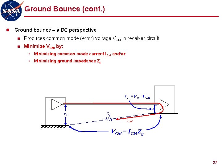
Ground Bounce (cont. ) l Ground bounce – a DC perspective n Produces common mode (error) voltage VCM in receiver circuit n Minimize VCM by: • Minimizing common mode current ICM and/or • Minimizing ground impedance Zg VI = VO - VCM VO Zg ICM VCM = ICM Zg 27

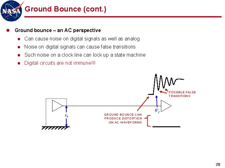
Ground Bounce (cont. ) l Ground bounce – an AC perspective n Can cause noise on digital signals as well as analog n Noise on digital signals can cause false transitions n Such noise on a clock line can lock up a state machine n Digital circuits are not immune!!! POSSIBLE FALSE TRANSITIONS VO GROUND BOUNCE CAN PRODUCE DISTORTION ON AC WAVEFORMS VI 28

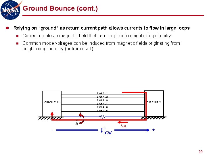
Ground Bounce (cont. ) l Relying on “ground” as return current path allows currents to flow in large loops n Current creates a magnetic field that can couple into neighboring circuitry n Common mode voltages can be induced from magnetic fields originating from neighboring circuitry (or from itself) CIRCUIT 1 - SIGNAL 1 SIGNAL 2 SIGNAL 3 SIGNAL 4 SIGNAL 5 SIGNAL 6 VCM CIRCUIT 2 ICM + 29

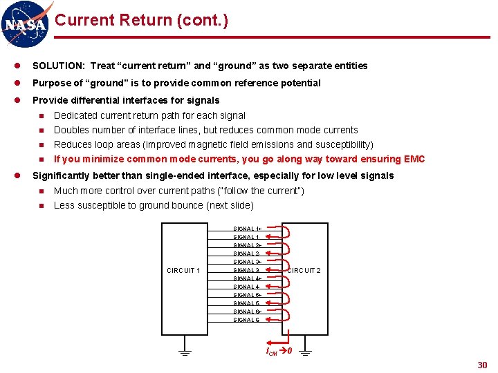
Current Return (cont. ) l SOLUTION: Treat “current return” and “ground” as two separate entities l Purpose of “ground” is to provide common reference potential l Provide differential interfaces for signals n Dedicated current return path for each signal Doubles number of interface lines, but reduces common mode currents Reduces loop areas (improved magnetic field emissions and susceptibility) n If you minimize common mode currents, you go along way toward ensuring EMC n n l Significantly better than single-ended interface, especially for low level signals n n Much more control over current paths (“follow the current”) Less susceptible to ground bounce (next slide) CIRCUIT 1 SIGNAL 1+ SIGNAL 1 SIGNAL 2+ SIGNAL 2 SIGNAL 3+ SIGNAL 3 SIGNAL 4+ SIGNAL 4 SIGNAL 5+ SIGNAL 5 SIGNAL 6+ SIGNAL 6 - CIRCUIT 2 ICM 0 30

If You Remember Nothing Else From Today… DO YOU KNOW WHERE YOUR CURRENTS ARE FLOWING? 31

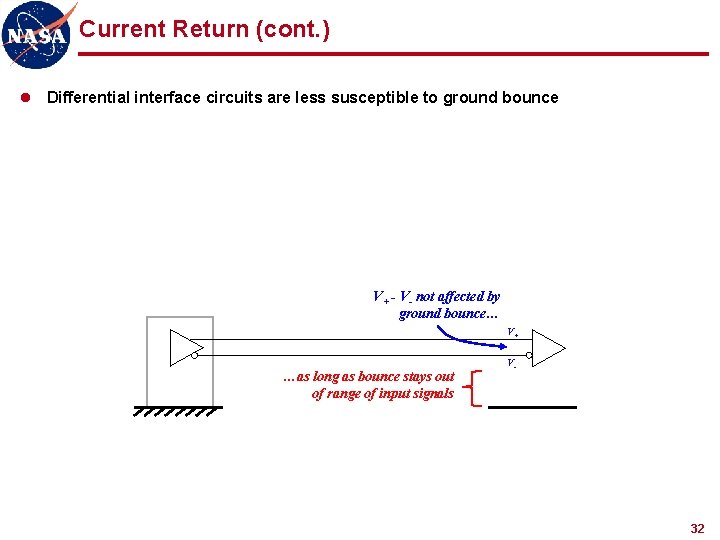
Current Return (cont. ) l Differential interface circuits are less susceptible to ground bounce V+ - V- not affected by ground bounce… V+ …as long as bounce stays out of range of input signals V- 32

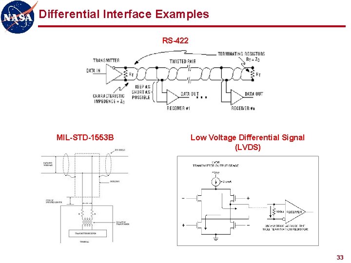
Differential Interface Examples RS-422 MIL-STD-1553 B Low Voltage Differential Signal (LVDS) 33

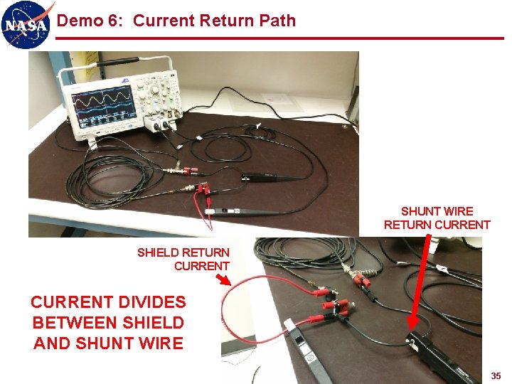
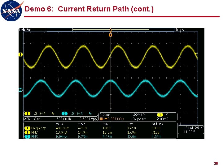
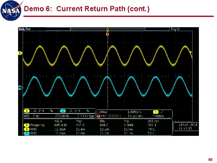
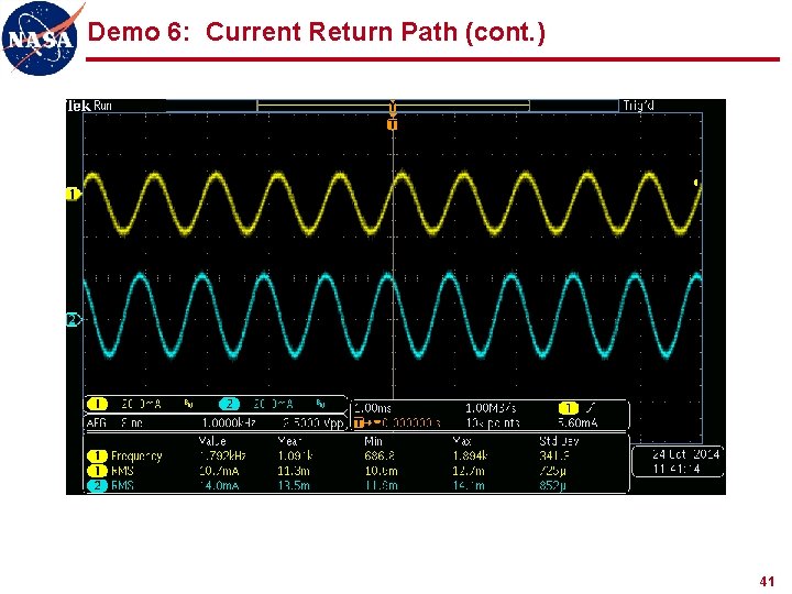
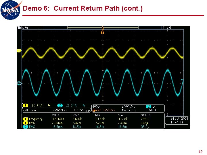
Demo 6: Current Return Path l DEMO/TUTORIAL: Current Return: The Path of Least IMPEDANCE n Video and full presentation on NESC Academy website: • http: //nescacademy. nasa. gov/ n Link on GSFC EMC Working Group XSPACES page: • https: //xspaces. gsfc. nasa. gov/display/EMCWG/Tutorials n Summary on following slides 34

Demo 6: Current Return Path SHUNT WIRE RETURN CURRENT SHIELD RETURN CURRENT DIVIDES BETWEEN SHIELD AND SHUNT WIRE 35

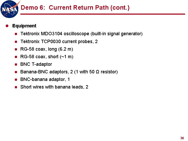
Demo 6: Current Return Path (cont. ) l Equipment n Tektronix MDO 3104 oscilloscope (built-in signal generator) n Tektronix TCP 0030 current probes, 2 n RG-58 coax, long (6. 2 m) n RG-58 coax, short (~1 m) n BNC T-adaptor n Banana-BNC adaptors, 2 (1 with 50 Ω resistor) n BNC-banana adaptor, 1 n Short wires with banana leads, 2 36

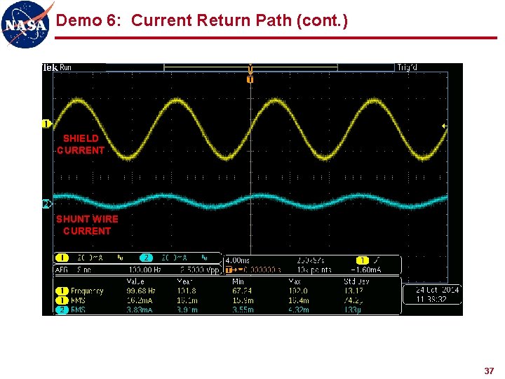
Demo 6: Current Return Path (cont. ) SHIELD CURRENT SHUNT WIRE CURRENT 37

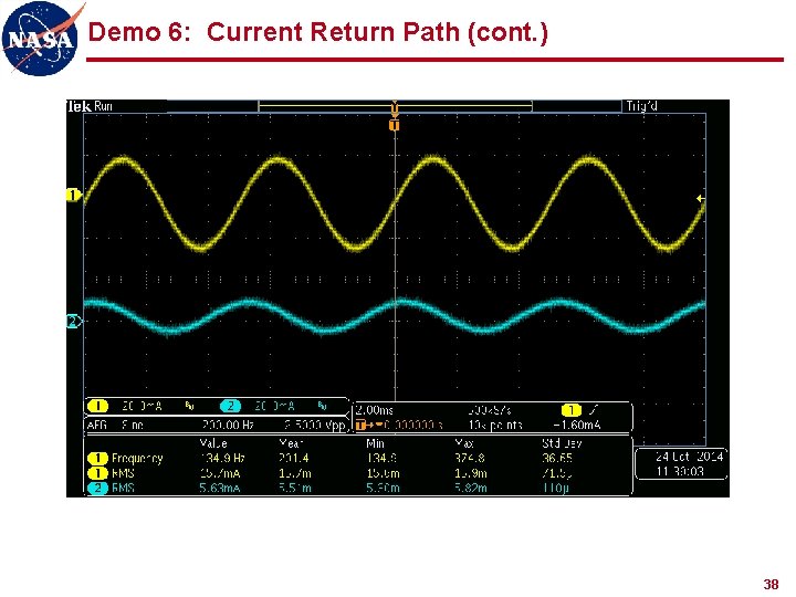
Demo 6: Current Return Path (cont. ) 38

Demo 6: Current Return Path (cont. ) 39

Demo 6: Current Return Path (cont. ) 40

Demo 6: Current Return Path (cont. ) 41

Demo 6: Current Return Path (cont. ) 42

Demo 6: Current Return Path (cont. ) 43

Demo 6: Current Return Path (cont. ) 44

Demo 6: Current Return Path (cont. ) 45

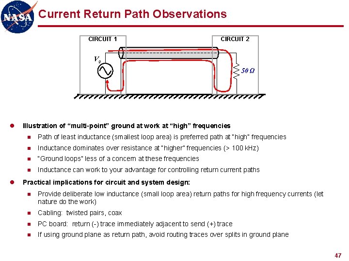
Kirchhoff’s Current Law l All currents return to their sources following path of least IMPEDANCE n NOT always path of least resistance l Currents do NOT return to ground n They may use ground as the return path to their source, if that is the path of least impedance BIG Rule of Thumb for EMC: “Follow the current” 46

Current Return Path Observations CIRCUIT 1 CIRCUIT 2 V 0 50 Ω l l Illustration of “multi-point” ground at work at “high” frequencies n Path of least inductance (smallest loop area) is preferred path at “high” frequencies n Inductance dominates over resistance at “higher” frequencies (> 100 k. Hz) n “Ground loops” less of a concern at these frequencies n Inductance can work to your advantage for controlling return current paths Practical implications for circuit and system design: n Provide deliberate low inductance (small loop area) return paths for high frequency currents (let nature do the work) n Cabling: twisted pairs, coax n PC board: return (-) trace immediately adjacent to send (+) trace n If using ground plane as return path, avoid routing traces over splits in ground plane 47

If You Remember Nothing Else From Today… DO YOU KNOW WHERE YOUR CURRENTS ARE FLOWING? 48

Topics l Introduction l Reasons for “Grounding” l “Grounding” in the “Real World” (and in “Real Space”) l Bonding 49

Bonding l Remember… n A poor (high impedance) bond will limit fault current n Hardware can be damaged without blowing fuse (bad) FUSE MAY NOT CLEAR (BAD) VS RL HIGH IMPEDANCE BOND FAULT CURRENT RETURN PATH 50

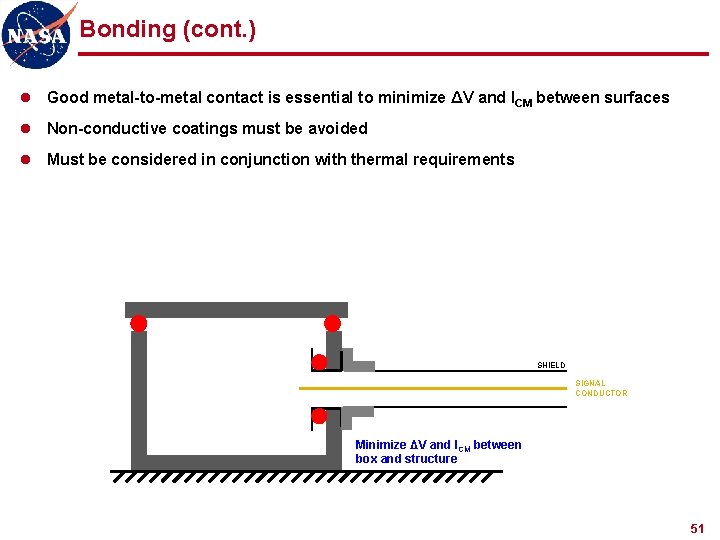
Bonding (cont. ) l Good metal-to-metal contact is essential to minimize ΔV and ICM between surfaces l Non-conductive coatings must be avoided l Must be considered in conjunction with thermal requirements SHIELD SIGNAL CONDUCTOR Minimize ΔV and ICM between box and structure 51

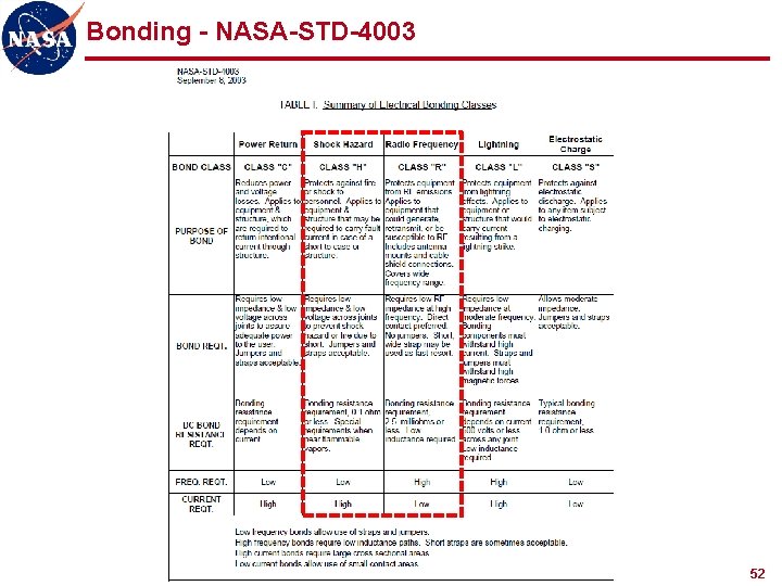
Bonding - NASA-STD-4003 52

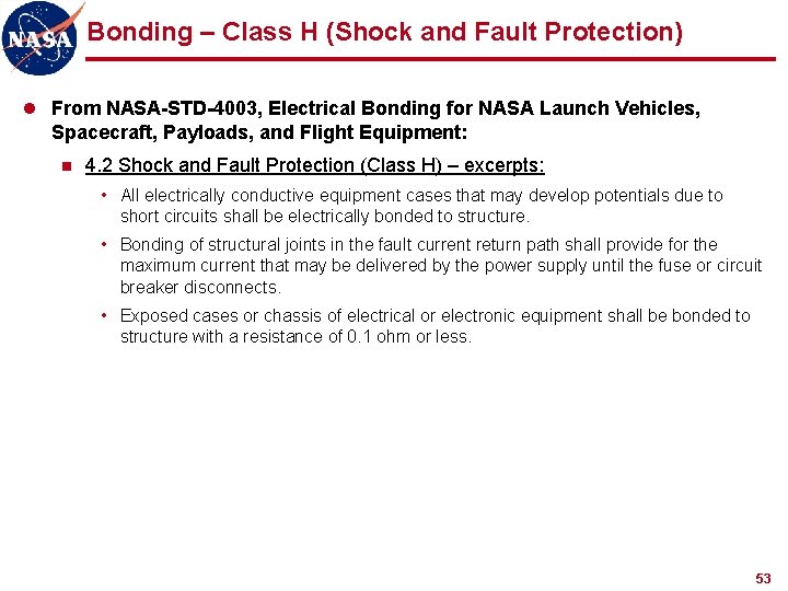
Bonding – Class H (Shock and Fault Protection) l From NASA-STD-4003, Electrical Bonding for NASA Launch Vehicles, Spacecraft, Payloads, and Flight Equipment: n 4. 2 Shock and Fault Protection (Class H) – excerpts: • All electrically conductive equipment cases that may develop potentials due to short circuits shall be electrically bonded to structure. • Bonding of structural joints in the fault current return path shall provide for the maximum current that may be delivered by the power supply until the fuse or circuit breaker disconnects. • Exposed cases or chassis of electrical or electronic equipment shall be bonded to structure with a resistance of 0. 1 ohm or less. 53

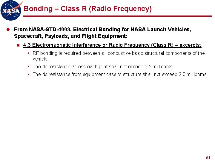
Bonding – Class R (Radio Frequency) l From NASA-STD-4003, Electrical Bonding for NASA Launch Vehicles, Spacecraft, Payloads, and Flight Equipment: n 4. 3 Electromagnetic Interference or Radio Frequency (Class R) – excerpts: • RF bonding is required between all conductive basic structural components of the vehicle. • The dc resistance across each joint shall not exceed 2. 5 milliohms. • The dc resistance from equipment case to structure shall not exceed 2. 5 milliohms. 54

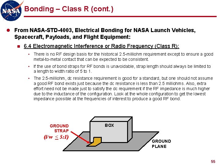
Bonding – Class R (cont. ) l From NASA-STD-4003, Electrical Bonding for NASA Launch Vehicles, Spacecraft, Payloads, and Flight Equipment: n 6. 4 Electromagnetic Interference or Radio Frequency (Class R): • There is no RF design basis for the historical 2. 5 -milliohm requirement except to ensure a good metal-to-metal contact that can be expected to be consistent. • If the use of bond straps for RF bonds is unavoidable, strap length should always be limited to a length to width ratio of 5 to 1. • The 2. 5 -milliohm, dc resistance requirement is good for a standard, but one should not assume a good RF bond exists just because the dc resistance is less than 2. 5 milliohms. Also, extra effort need not be made just to satisfy the dc requirement if the RF impedance is much higher due to the inductance of the configuration. Look at the whole configuration to get the lowest impedance possible at the frequencies of interest to produce a good RF bond. GROUND STRAP (l/w < 5: 1) BOX GROUND PLANE 55

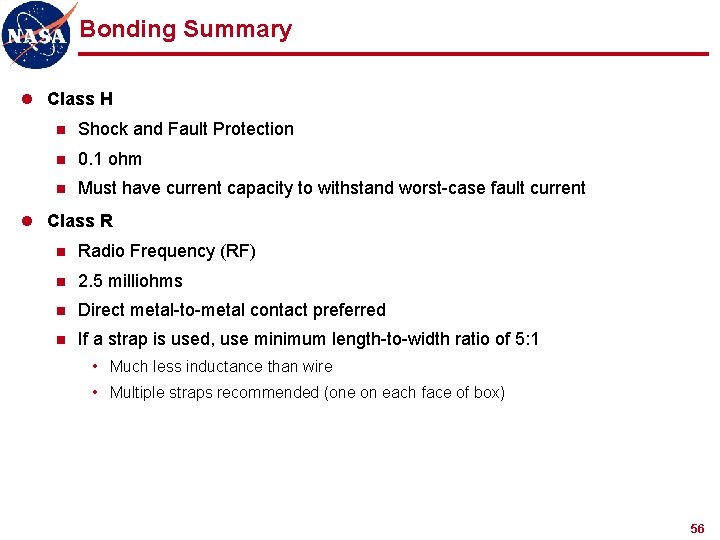
Bonding Summary l Class H n Shock and Fault Protection n 0. 1 ohm n Must have current capacity to withstand worst-case fault current l Class R n Radio Frequency (RF) n 2. 5 milliohms n Direct metal-to-metal contact preferred n If a strap is used, use minimum length-to-width ratio of 5: 1 • Much less inductance than wire • Multiple straps recommended (one on each face of box) 56

If You Remember Nothing Else From Today… DO YOU KNOW WHERE YOUR CURRENTS ARE FLOWING? 57