CS 61 C Great Ideas in Computer Architecture

- Slides: 49

CS 61 C: Great Ideas in Computer Architecture (Machine Structures) Switches, Transistors, Gates, Flip-Flops Instructor: Michael Greenbaum 10/2/2020 Summer 2011 -- Lecture 18 1

Review • Sequential software is slow software – SIMD and MIMD only path to higher performance • Multiprocessor/Multicore uses Shared Memory – Cache coherency implements shared memory even with multiple copies in multiple caches – False sharing a concern; watch block size! • Data races lead to subtle parallel bugs • Synchronization via atomic operations: – MIPS does it with Load Linked + Store Conditional • Open. MP as simple parallel extension to C – Threads, Parallel for, private, critical sections, … 10/2/2020 Summer 2011 -- Lecture 18 2

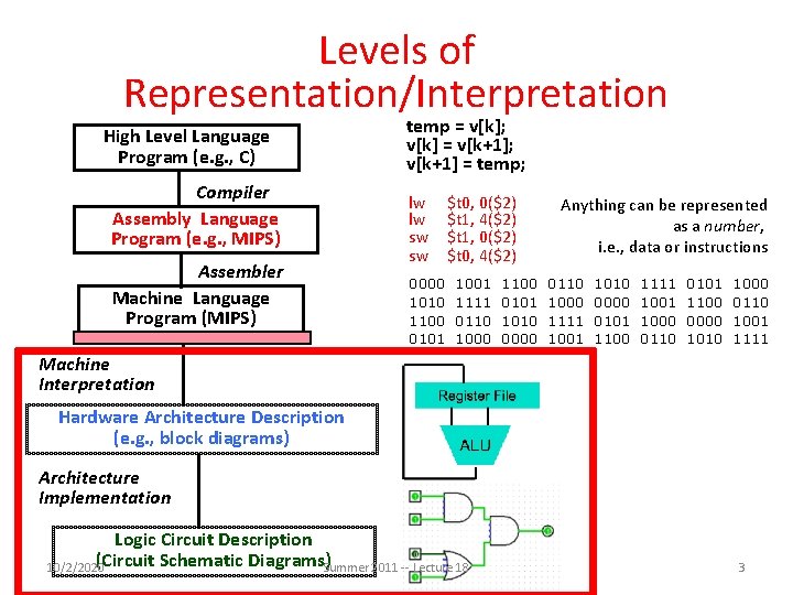
Levels of Representation/Interpretation High Level Language Program (e. g. , C) Compiler Assembly Language Program (e. g. , MIPS) Assembler Machine Language Program (MIPS) temp = v[k]; v[k] = v[k+1]; v[k+1] = temp; lw lw sw sw 0000 1010 1100 0101 $t 0, 0($2) $t 1, 4($2) $t 1, 0($2) $t 0, 4($2) 1001 1111 0110 1000 1100 0101 1010 0000 Anything can be represented as a number, i. e. , data or instructions 0110 1000 1111 1001 1010 0000 0101 1100 1111 1000 0110 0101 1100 0000 1010 1000 0110 1001 1111 Machine Interpretation Hardware Architecture Description (e. g. , block diagrams) Architecture Implementation Logic Circuit Description (Circuit Schematic Diagrams)Summer 2011 -- Lecture 18 10/2/2020 3

Agenda • • Switching Networks, Transistors Administrivia Combinational Logic Break Combinational Logic (cont'd) State Elements Summary 10/2/2020 Fall 2010 -- Lecture #22 4

Hardware Design • Next several weeks: we’ll study how a modern processor is built; starting with basic elements as building blocks • Why study hardware design? – Understand capabilities and limitations of hw in general and processors in particular – What processors can do fast and what they can’t do fast (avoid slow things if you want your code to run fast!) – Background for more in depth hw courses (CS 150, CS 152) – There is just so much you can do with standard processors: you may need to design own custom hw for extra performance – Even some commercial processors today have customizable hardware! 10/2/2020 Summer 2011 -- Lecture 18 5

Synchronous Digital Systems Hardware of a processor, such as the MIPS, is an example of a Synchronous Digital System Synchronous: • All operations coordinated by a central clock § “Heartbeat” of the system! Digital: • Represent All values by 2 discrete values • Electrical signals are treated as 1’s and 0’s • 1 and 0 are complements of each other • High /low voltage for true / false, 1 / 0 10/2/2020 Summer 2011 -- Lecture 18 6

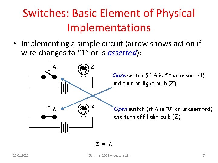
Switches: Basic Element of Physical Implementations • Implementing a simple circuit (arrow shows action if wire changes to “ 1” or is asserted): A Z Close switch (if A is “ 1” or asserted) and turn on light bulb (Z) A Z Open switch (if A is “ 0” or unasserted) and turn off light bulb (Z) Z A 10/2/2020 Summer 2011 -- Lecture 18 7

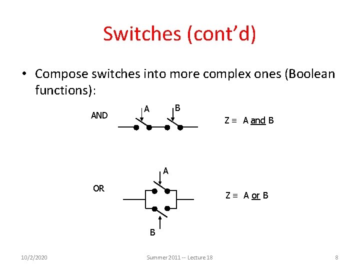
Switches (cont’d) • Compose switches into more complex ones (Boolean functions): AND B A Z A and B A OR Z A or B B 10/2/2020 Summer 2011 -- Lecture 18 8

Historical Note • Early computer designers built ad hoc circuits from switches • Began to notice common patterns in their work: ANDs, ORs, … • Master’s thesis (by Claude Shannon) made link between work and 19 th Century Mathematician George Boole – Called it “Boolean” in his honor • Could apply math to give theory to hardware design, minimization, … 10/2/2020 Summer 2011 -- Lecture 18 9

Transistor Networks • Modern digital systems designed in CMOS – MOS: Metal-Oxide on Semiconductor – C for complementary: use pairs of normally-open and normally-closed switches • CMOS transistors act as voltage-controlled switches – Similar, though easier to work with, than relay switches from earlier era 10/2/2020 Summer 2011 -- Lecture 18 10

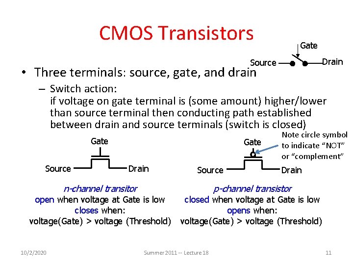
CMOS Transistors Gate Drain Source • Three terminals: source, gate, and drain – Switch action: if voltage on gate terminal is (some amount) higher/lower than source terminal then conducting path established between drain and source terminals (switch is closed) Gate Source Gate Drain Source Note circle symbol to indicate “NOT” or “complement” Drain n-channel transitor p-channel transistor open when voltage at Gate is low closes when: voltage(Gate) > voltage (Threshold) closed when voltage at Gate is low opens when: voltage(Gate) > voltage (Threshold) 10/2/2020 Summer 2011 -- Lecture 18 11

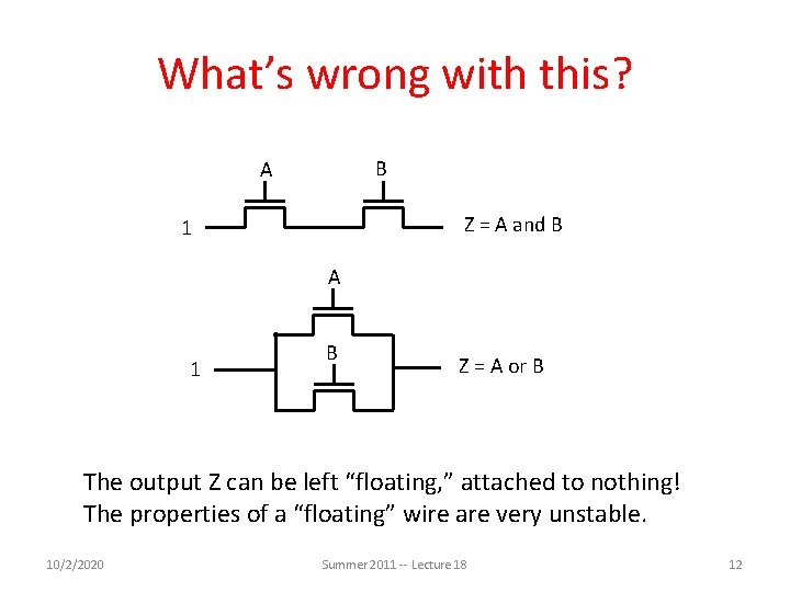
What’s wrong with this? B A Z = A and B 1 A 1 B Z = A or B The output Z can be left “floating, ” attached to nothing! The properties of a “floating” wire are very unstable. 10/2/2020 Summer 2011 -- Lecture 18 12

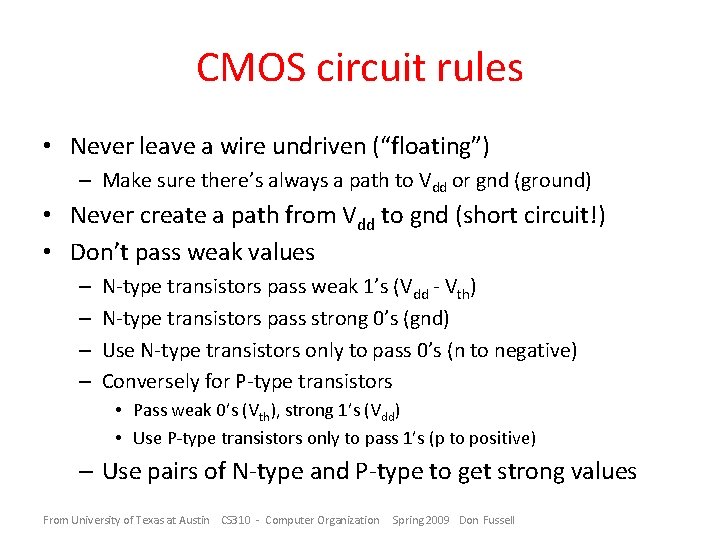
CMOS circuit rules • Never leave a wire undriven (“floating”) – Make sure there’s always a path to Vdd or gnd (ground) • Never create a path from Vdd to gnd (short circuit!) • Don’t pass weak values – – N-type transistors pass weak 1’s (Vdd - Vth) N-type transistors pass strong 0’s (gnd) Use N-type transistors only to pass 0’s (n to negative) Conversely for P-type transistors • Pass weak 0’s (Vth), strong 1’s (Vdd) • Use P-type transistors only to pass 1’s (p to positive) – Use pairs of N-type and P-type to get strong values From University of Texas at Austin CS 310 - Computer Organization Spring 2009 Don Fussell

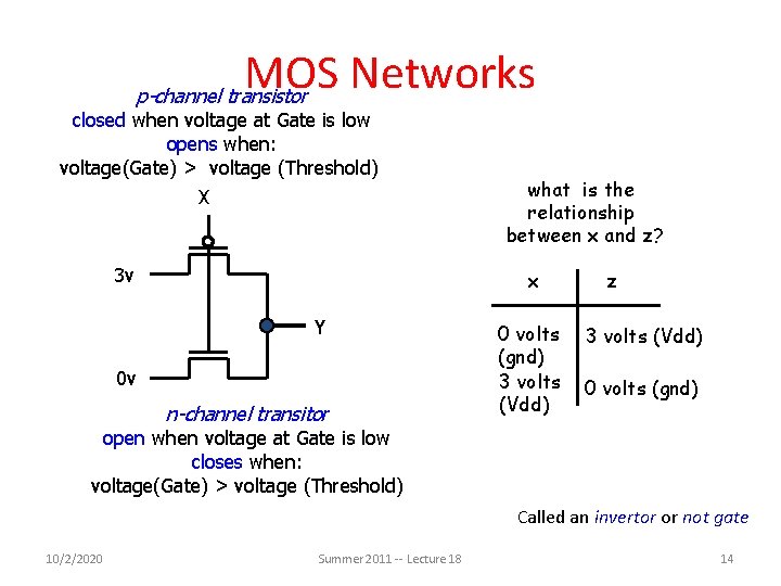
MOS Networks p-channel transistor closed when voltage at Gate is low opens when: voltage(Gate) > voltage (Threshold) X 3 v what is the relationship between x and z? x Y 0 v n-channel transitor 0 volts (gnd) 3 volts (Vdd) z 3 volts (Vdd) 0 volts (gnd) open when voltage at Gate is low closes when: voltage(Gate) > voltage (Threshold) Called an invertor or not gate 10/2/2020 Summer 2011 -- Lecture 18 14

Agenda • • Switching Networks, Transistors Administrivia Combinational Logic Break Combinational Logic (cont'd) State Elements Summary 10/2/2020 Fall 2010 -- Lecture #22 15

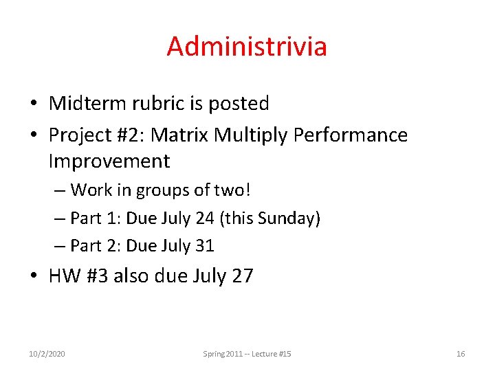
Administrivia • Midterm rubric is posted • Project #2: Matrix Multiply Performance Improvement – Work in groups of two! – Part 1: Due July 24 (this Sunday) – Part 2: Due July 31 • HW #3 also due July 27 10/2/2020 Spring 2011 -- Lecture #15 16

Agenda • • Switching Networks, Transistors Administrivia Combinational Logic Break Combinational Logic (cont'd) State Elements Summary 10/2/2020 Fall 2010 -- Lecture #22 17

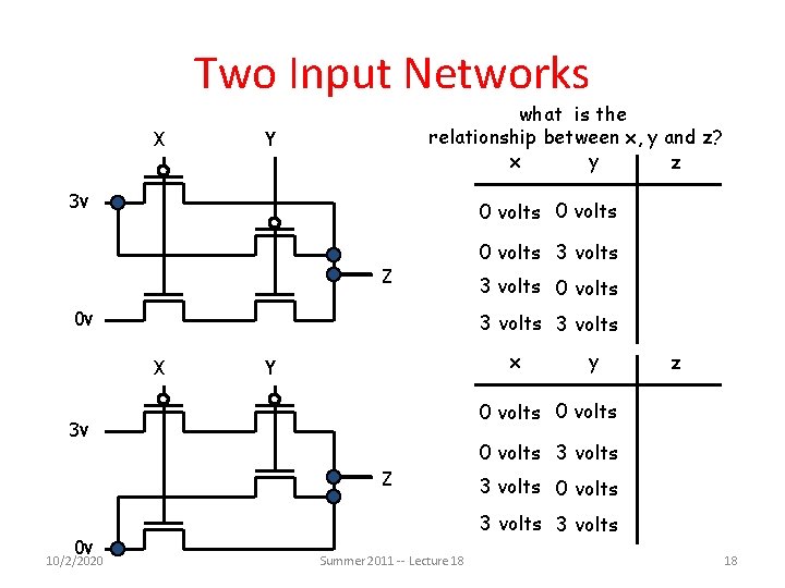
Two Input Networks X what is the relationship between x, y and z? x y z Y 3 v 0 volts Z 0 v x Y y z 0 volts 3 v 0 volts 3 volts Z 0 v 3 volts 0 volts 3 volts X 10/2/2020 0 volts 3 volts Summer 2011 -- Lecture 18 18

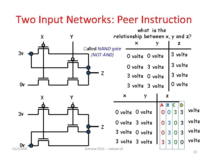
Two Input Networks: Peer Instruction X Y 3 v what is the relationship between x, y and z? x y z Called NAND gate (NOT AND) 0 volts 3 volts Z 0 v X x Y Z 0 v 3 volts 0 volts 3 volts 0 volts y 0 volts 3 v 10/2/2020 0 volts 3 volts z A B C D 0 0 3 3 volts 0 3 0 3 volts 3 3 0 0 volts 3 volts Summer 2011 -- Lecture 18 19

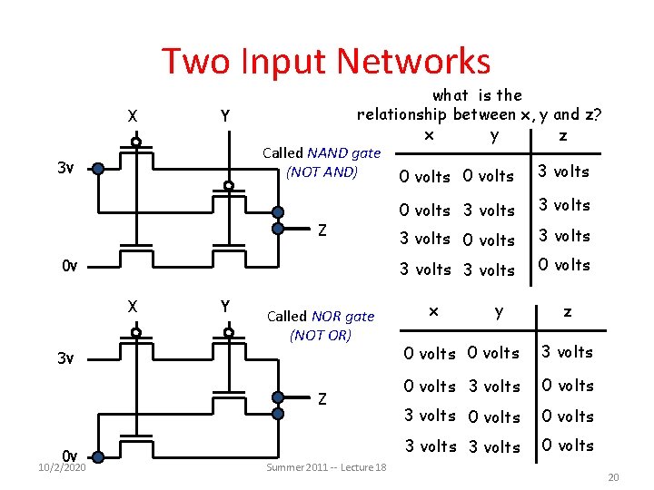
Two Input Networks X Y 3 v what is the relationship between x, y and z? x y z Called NAND gate (NOT AND) 0 volts 3 volts Z 0 v X Y Called NOR gate (NOT OR) 3 v Z 0 v 10/2/2020 Summer 2011 -- Lecture 18 0 volts 3 volts 3 volts 0 volts x y z 0 volts 3 volts 0 volts 3 volts 0 volts 20

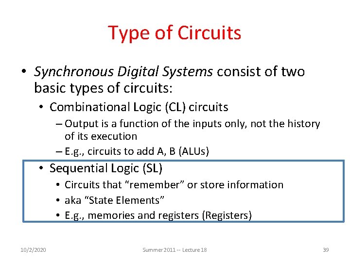
Type of Circuits • Synchronous Digital Systems consist of two basic types of circuits: • Combinational Logic (CL) circuits – Output is a function of the inputs only, not the history of its execution – E. g. , circuits to add A, B (ALUs) • Sequential Logic (SL) • Circuits that “remember” or store information • aka “State Elements” • E. g. , memories and registers (Registers) 10/2/2020 Summer 2011 -- Lecture 18 21

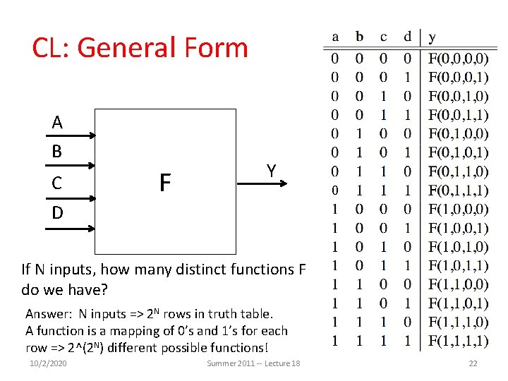
CL: General Form A B C D F Y 0 If N inputs, how many distinct functions F do we have? Answer: N inputs => 2 N rows in truth table. A function is a mapping of 0’s and 1’s for each row => 2^(2 N) different possible functions! 10/2/2020 Summer 2011 -- Lecture 18 22

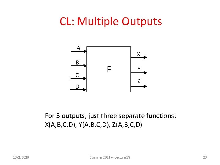
CL: Multiple Outputs A B C X F Y Z D For 3 outputs, just three separate functions: X(A, B, C, D), Y(A, B, C, D), Z(A, B, C, D) 10/2/2020 Summer 2011 -- Lecture 18 23

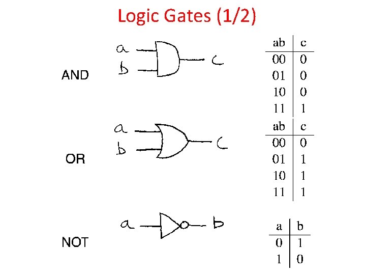
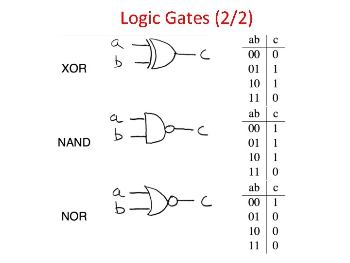
Logic Gates • A few of the functions on 1 and 2 inputs are given names and special symbols when drawn out: 10/2/2020 Summer 2011 -- Lecture 18 24

Logic Gates (1/2)

Logic Gates (2/2)

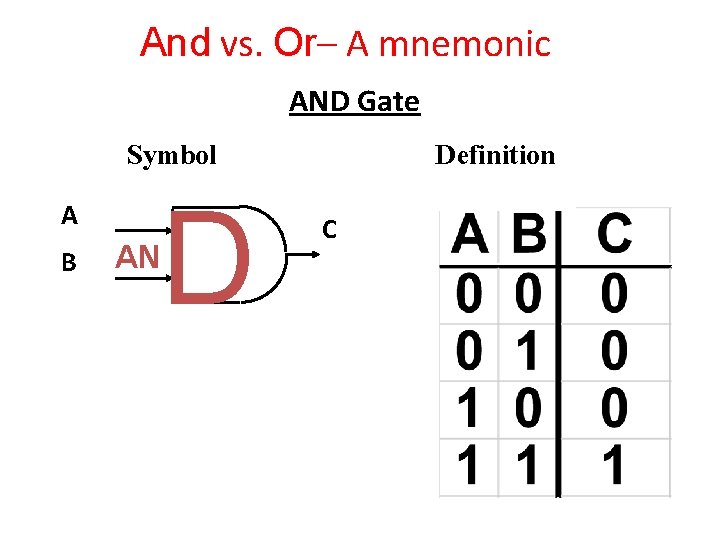
And vs. Or– A mnemonic AND Gate Symbol A B AN D Definition C

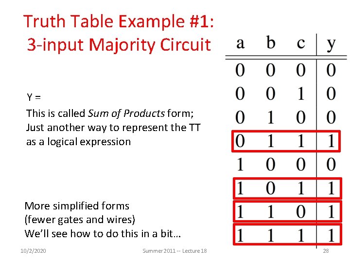
Truth Table Example #1: 3 -input Majority Circuit Y=ABC + ABC This is called Sum of Products form; Just another way to represent the TT as a logical expression Y = B C + A (B C + B C) Y = B C + A (B + C) More simplified forms (fewer gates and wires) We’ll see how to do this in a bit… 10/2/2020 Summer 2011 -- Lecture 18 28

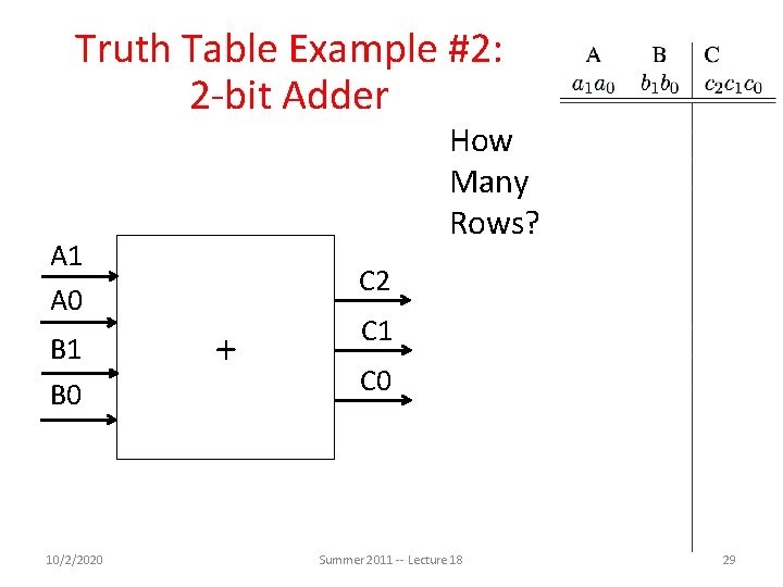
Truth Table Example #2: 2 -bit Adder How Many Rows? A 1 A 0 B 1 B 0 10/2/2020 C 2 + C 1 C 0 Summer 2011 -- Lecture 18 29

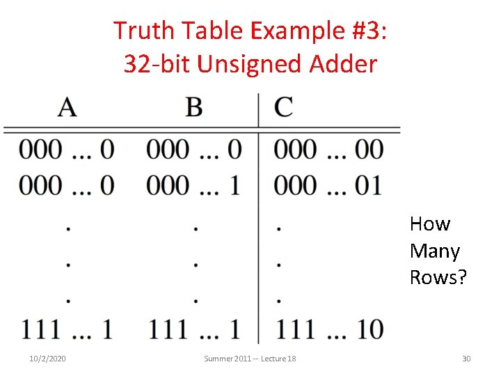
Truth Table Example #3: 32 -bit Unsigned Adder How Many Rows? 10/2/2020 Summer 2011 -- Lecture 18 30

Agenda • • Switching Networks, Transistors Administrivia Combinational Logic Break Combinational Logic (cont'd) State Elements Summary 10/2/2020 Fall 2010 -- Lecture #22 31

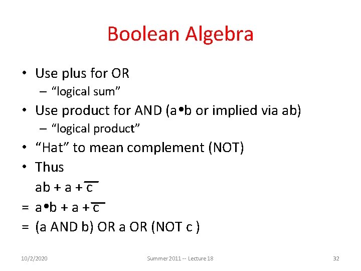
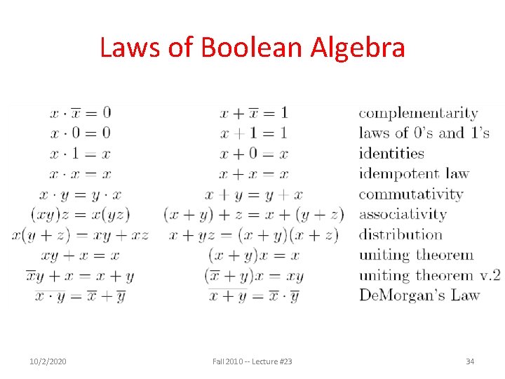
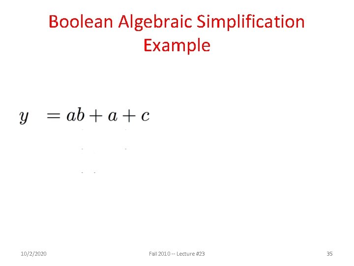
Boolean Algebra • Use plus for OR – “logical sum” • Use product for AND (a b or implied via ab) – “logical product” • “Hat” to mean complement (NOT) • Thus ab + a + c = a b + a + c = (a AND b) OR a OR (NOT c ) 10/2/2020 Summer 2011 -- Lecture 18 32

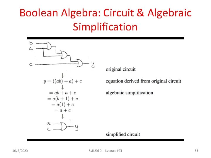
Boolean Algebra: Circuit & Algebraic Simplification 10/2/2020 Fall 2010 -- Lecture #23 33

Laws of Boolean Algebra 10/2/2020 Fall 2010 -- Lecture #23 34

Boolean Algebraic Simplification Example 10/2/2020 Fall 2010 -- Lecture #23 35

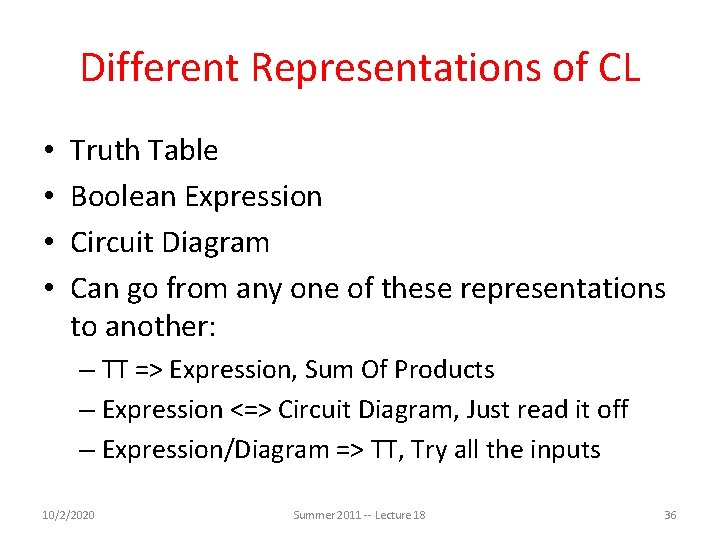
Different Representations of CL • • Truth Table Boolean Expression Circuit Diagram Can go from any one of these representations to another: – TT => Expression, Sum Of Products – Expression <=> Circuit Diagram, Just read it off – Expression/Diagram => TT, Try all the inputs 10/2/2020 Summer 2011 -- Lecture 18 36

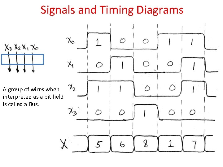
Signals and Timing Diagrams A group of wires when interpreted as a bit field is called a Bus.

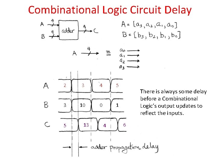
Combinational Logic Circuit Delay 2 3 4 5 3 10 0 1 5 13 4 There is always some delay before a Combinational Logic’s output updates to reflect the inputs. 6

Type of Circuits • Synchronous Digital Systems consist of two basic types of circuits: • Combinational Logic (CL) circuits – Output is a function of the inputs only, not the history of its execution – E. g. , circuits to add A, B (ALUs) • Sequential Logic (SL) • Circuits that “remember” or store information • aka “State Elements” • E. g. , memories and registers (Registers) 10/2/2020 Summer 2011 -- Lecture 18 39

Uses for State Elements • Place to store values for some amount of time: – Register files (like $1 -$31 on the MIPS) – Memory (caches, and main memory) • Help control flow of information between combinational logic blocks – State elements are used to hold up the movement of information at the inputs to combinational logic blocks and allow for orderly passage 10/2/2020 Fall 2010 -- Lecture #23 40

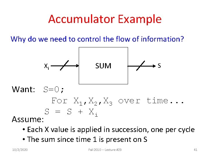
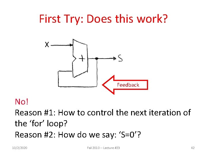
Accumulator Example Why do we need to control the flow of information? Xi SUM S Want: S=0; For X 1, X 2, X 3 over time. . . S = S + Xi Assume: • Each X value is applied in succession, one per cycle • The sum since time 1 is present on S 10/2/2020 Fall 2010 -- Lecture #23 41

First Try: Does this work? X Feedback No! Reason #1: How to control the next iteration of the ‘for’ loop? Reason #2: How do we say: ‘S=0’? 10/2/2020 Fall 2010 -- Lecture #23 42

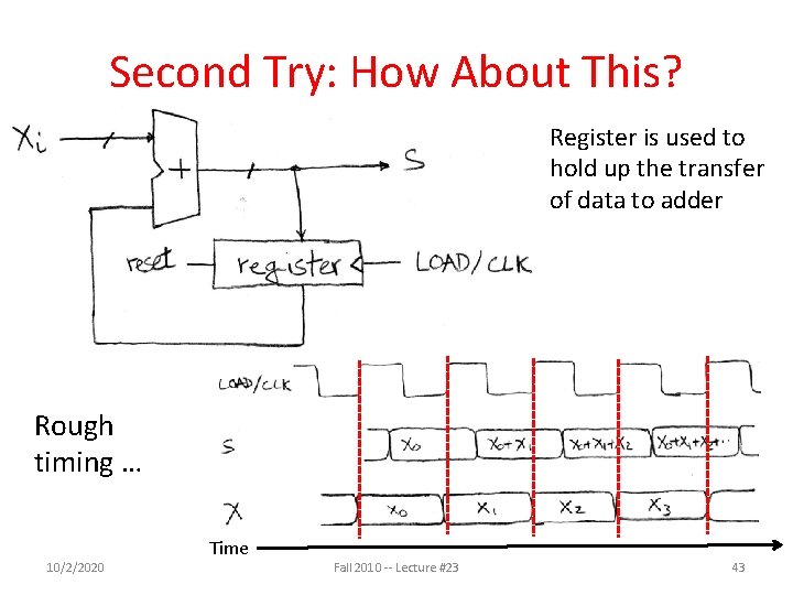
Second Try: How About This? Register is used to hold up the transfer of data to adder Rough timing … 10/2/2020 Time Fall 2010 -- Lecture #23 43

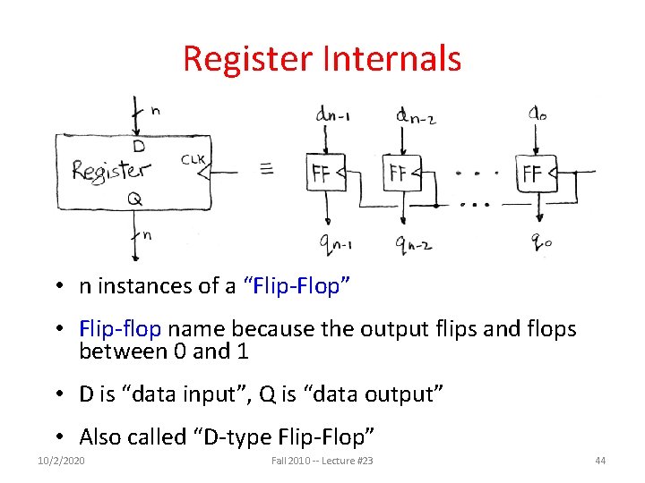
Register Internals • n instances of a “Flip-Flop” • Flip-flop name because the output flips and flops between 0 and 1 • D is “data input”, Q is “data output” • Also called “D-type Flip-Flop” 10/2/2020 Fall 2010 -- Lecture #23 44

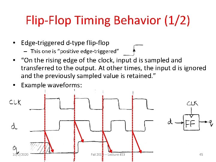
Flip-Flop Timing Behavior (1/2) • Edge-triggered d-type flip-flop – This one is “positive edge-triggered” • “On the rising edge of the clock, input d is sampled and transferred to the output. At other times, the input d is ignored and the previously sampled value is retained. ” • Example waveforms: 10/2/2020 Fall 2010 -- Lecture #23 45

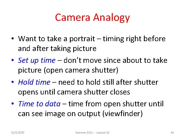
Camera Analogy • Want to take a portrait – timing right before and after taking picture • Set up time – don’t move since about to take picture (open camera shutter) • Hold time – need to hold still after shutter opens until camera shutter closes • Time to data – time from open shutter until can see image on output (viewfinder) 10/2/2020 Summer 2011 -- Lecture 18 46

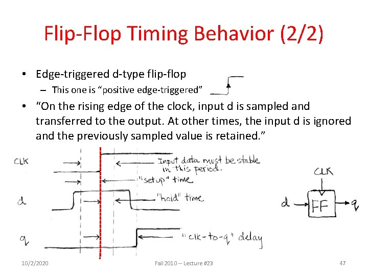
Flip-Flop Timing Behavior (2/2) • Edge-triggered d-type flip-flop – This one is “positive edge-triggered” • “On the rising edge of the clock, input d is sampled and transferred to the output. At other times, the input d is ignored and the previously sampled value is retained. ” 10/2/2020 Fall 2010 -- Lecture #23 47

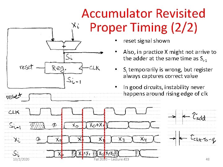
Accumulator Revisited Proper Timing (2/2) • reset signal shown • Also, in practice X might not arrive to the adder at the same time as Si-1 • Si temporarily is wrong, but register always captures correct value • In good circuits, instability never happens around rising edge of clk 10/2/2020 Fall 2010 -- Lecture #23 48

“And In Conclusion. . ” • Hardware systems are constructed from Stateless Combinational Logic and Stateful “Memory” Logic (Registers) • Real world voltages are analog, but are quantized to represent logic 0 and logic 1 • Alternate representations for Combinational Logic: Truth table, boolean expression, gates • Boolean Algebra allows minimization of gates • State registers implemented from Flip-flops 10/2/2020 Summer 2011 -- Lecture 18 49