CS 61 C Great Ideas in Computer Architecture

- Slides: 62

CS 61 C: Great Ideas in Computer Architecture Introduction to Hardware: Representations and State Instructor: Randy H. Katz http: //inst. eecs. Berkeley. edu/~cs 61 c/fa 13 9/30/2020 Fall 2013 -- Lecture #17 1

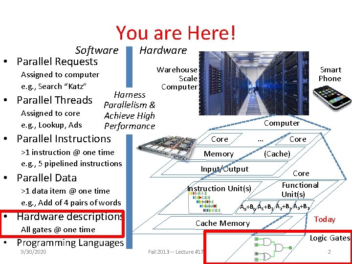
You are Here! Software • Parallel Requests Assigned to computer e. g. , Search “Katz” • Parallel Threads Assigned to core e. g. , Lookup, Ads Hardware Harness Parallelism & Achieve High Performance Smart Phone Warehouse Scale Computer • Parallel Instructions >1 instruction @ one time e. g. , 5 pipelined instructions • Parallel Data >1 data item @ one time e. g. , Add of 4 pairs of words • Hardware descriptions All gates @ one time • Programming Languages 9/30/2020 … Core Memory Core (Cache) Input/Output Instruction Unit(s) Core Functional Unit(s) A 0+B 0 A 1+B 1 A 2+B 2 A 3+B 3 Cache Memory Today Logic Gates Fall 2013 -- Lecture #17 2

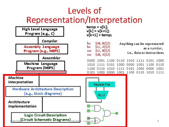
Levels of Representation/Interpretation High Level Language Program (e. g. , C) Compiler Assembly Language Program (e. g. , MIPS) Assembler Machine Language Program (MIPS) temp = v[k]; v[k] = v[k+1]; v[k+1] = temp; lw lw sw sw 0000 1010 1100 0101 $t 0, 0($2) $t 1, 4($2) $t 1, 0($2) $t 0, 4($2) 1001 1111 0110 1000 1100 0101 1010 0000 Anything can be represented as a number, i. e. , data or instructions 0110 1000 1111 1001 1010 0000 0101 1100 1111 1000 0110 0101 1100 0000 1010 1000 0110 1001 1111 Machine Interpretation Hardware Architecture Description (e. g. , block diagrams) Architecture Implementation Logic Circuit Description (Circuit Schematic Diagrams) Fall 2013 -- Lecture #17 9/30/2020 3

Agenda • • • Switching Networks, Transistors Gates and Truth Tables for Circuits Boolean Algebra Logisim State Machines And in Conclusion, … 9/30/2020 Fall 2013 -- Lecture #17 4

Agenda • • • Switching Networks, Transistors Gates and Truth Tables for Circuits Boolean Algebra Logisim State Machines And in Conclusion, … 9/30/2020 Fall 2013 -- Lecture #17 5

Hardware Design • Next several weeks: how a modern processor is built, starting with basic elements as building blocks • Why study hardware design? – Understand capabilities and limitations of hw in general and processors in particular – What processors can do fast and what they can’t do fast (avoid slow things if you want your code to run fast!) – Background for more in depth hw courses (CS 152) – Hard to know what will need for next 30 years – There is just so much you can do with standard processors: you may need to design own custom hw for extra performance – Even some commercial processors today have customizable hardware! 9/30/2020 Fall 2013 -- Lecture #17 6

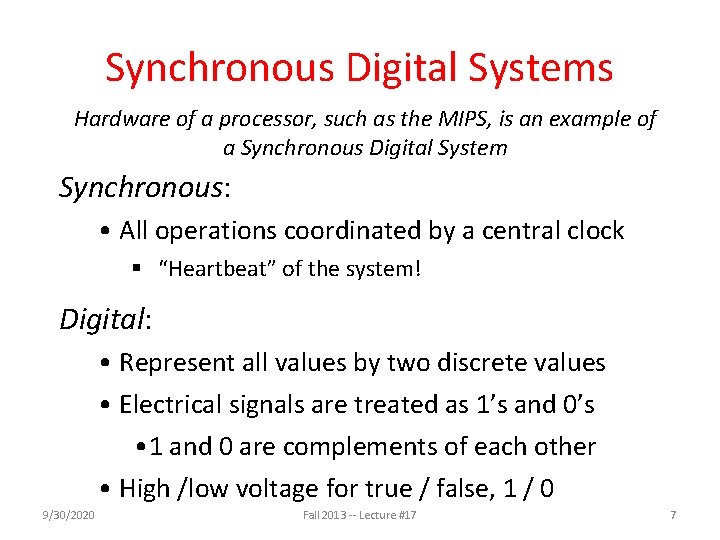
Synchronous Digital Systems Hardware of a processor, such as the MIPS, is an example of a Synchronous Digital System Synchronous: • All operations coordinated by a central clock § “Heartbeat” of the system! Digital: • Represent all values by two discrete values • Electrical signals are treated as 1’s and 0’s • 1 and 0 are complements of each other • High /low voltage for true / false, 1 / 0 9/30/2020 Fall 2013 -- Lecture #17 7

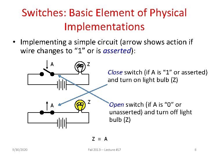
Switches: Basic Element of Physical Implementations • Implementing a simple circuit (arrow shows action if wire changes to “ 1” or is asserted): A Z Close switch (if A is “ 1” or asserted) and turn on light bulb (Z) A Z Open switch (if A is “ 0” or unasserted) and turn off light bulb (Z) Z A 9/30/2020 Fall 2013 -- Lecture #17 8

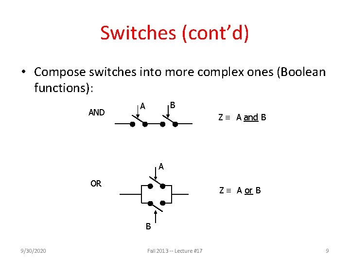
Switches (cont’d) • Compose switches into more complex ones (Boolean functions): AND B A Z A and B A OR Z A or B B 9/30/2020 Fall 2013 -- Lecture #17 9

Historical Note • Early computer designers built ad hoc circuits from switches • Began to notice common patterns in their work: ANDs, ORs, … • Master’s thesis (by Claude Shannon) made link between work and 19 th Century Mathematician George Boole – Called it “Boolean” in his honor • Could apply math to give theory to hardware design, minimization, … 9/30/2020 Fall 2013 -- Lecture #17 10

Transistors High voltage (Vdd) represents 1, or true Low voltage (0 volts or Ground) represents 0, or false Let threshold voltage (Vth) decide if a 0 or a 1 If switches control whether voltages can propagate through a circuit, can build a computer • Our switches: CMOS transistors • • 9/30/2020 Fall 2013 -- Lecture #17 11

CMOS Transistor Networks • Modern digital systems designed in CMOS – MOS: Metal-Oxide on Semiconductor – C for complementary: use pairs of normally-open and normally-closed switches • Used to be called COS-MOS for complementary-symmetry MOS • CMOS transistors act as voltage-controlled switches – Similar, though easier to work with, than relay switches from earlier era – Use energy primarily when switching 9/30/2020 Fall 2013 -- Lecture #17 12

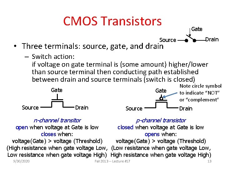
CMOS Transistors Gate Drain Source • Three terminals: source, gate, and drain – Switch action: if voltage on gate terminal is (some amount) higher/lower than source terminal then conducting path established between drain and source terminals (switch is closed) Gate Source Gate Drain Source n-channel transitor Note circle symbol to indicate “NOT” or “complement” Drain p-channel transistor open when voltage at Gate is low closed when voltage at Gate is low closes when: opens when: voltage(Gate) > voltage (Threshold) (High resistance when gate voltage Low, (Low resistance when gate voltage Low, Low resistance when gate voltage High) High resistance when gate voltage High) 9/30/2020 Fall 2013 -- Lecture #17 13

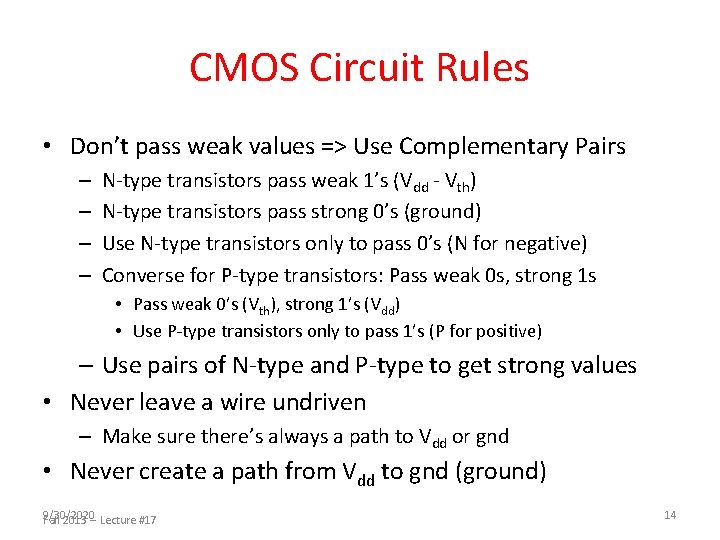
CMOS Circuit Rules • Don’t pass weak values => Use Complementary Pairs – – N-type transistors pass weak 1’s (Vdd - Vth) N-type transistors pass strong 0’s (ground) Use N-type transistors only to pass 0’s (N for negative) Converse for P-type transistors: Pass weak 0 s, strong 1 s • Pass weak 0’s (Vth), strong 1’s (Vdd) • Use P-type transistors only to pass 1’s (P for positive) – Use pairs of N-type and P-type to get strong values • Never leave a wire undriven – Make sure there’s always a path to Vdd or gnd • Never create a path from Vdd to gnd (ground) 9/30/2020 Fall 2013 -- Lecture #17 14

Administrivia 9/30/2020 Fall 2013 -- Lecture #17 15

Agenda • • • Switching Networks, Transistors Gates and Truth Tables for Circuits Boolean Algebra Logisim State Machines And in Conclusion, … 9/30/2020 Fall 2013 -- Lecture #17 16

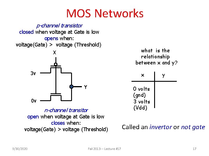
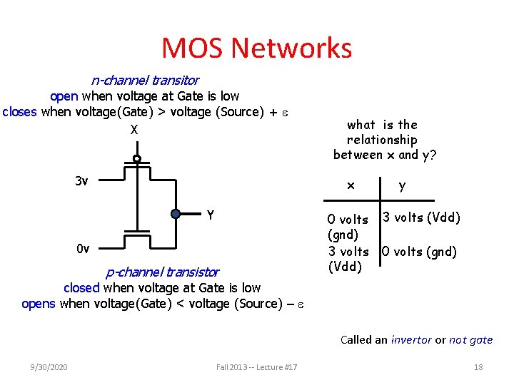
MOS Networks p-channel transistor closed when voltage at Gate is low opens when: voltage(Gate) > voltage (Threshold) X 3 v x Y y 0 volts (gnd) 3 volts (Vdd) 0 v n-channel transitor open when voltage at Gate is low closes when: voltage(Gate) > voltage (Threshold) 9/30/2020 what is the relationship between x and y? Fall 2013 -- Lecture #17 Called an invertor or not gate 17

MOS Networks n-channel transitor open when voltage at Gate is low closes when voltage(Gate) > voltage (Source) + X 3 v what is the relationship between x and y? x Y 0 v p-channel transistor 0 volts (gnd) 3 volts (Vdd) y 3 volts (Vdd) 0 volts (gnd) closed when voltage at Gate is low opens when voltage(Gate) < voltage (Source) – Called an invertor or not gate 9/30/2020 Fall 2013 -- Lecture #17 18

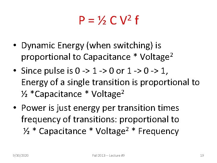
P = ½ C V 2 f • Dynamic Energy (when switching) is proportional to Capacitance * Voltage 2 • Since pulse is 0 -> 1 -> 0 or 1 -> 0 -> 1, Energy of a single transition is proportional to ½ *Capacitance * Voltage 2 • Power is just energy per transition times frequency of transitions: proportional to ½ * Capacitance * Voltage 2 * Frequency 9/30/2020 Fall 2013 -- Lecture #9 19

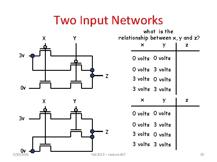
Two Input Networks X what is the relationship between x, y and z? x y z Y 3 v 0 volts Z 0 v x Y y z 0 volts 3 v 0 volts 3 volts Z 0 v 3 volts 0 volts 3 volts X 9/30/2020 0 volts 3 volts Fall 2013 -- Lecture #17 20

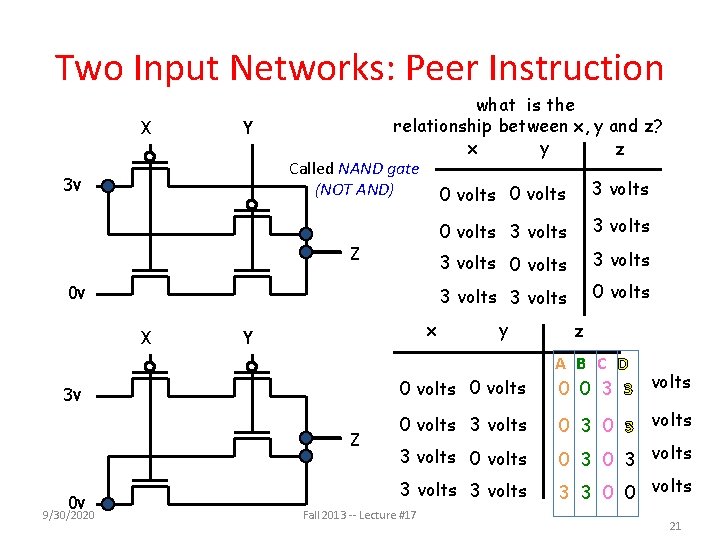
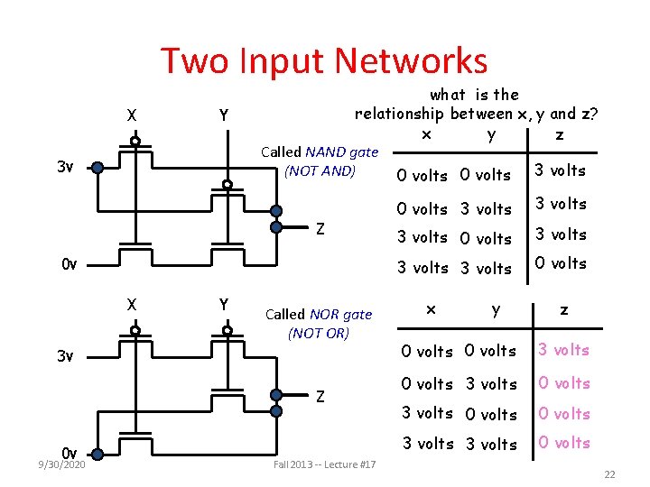
Two Input Networks: Peer Instruction X Y 3 v what is the relationship between x, y and z? x y z Called NAND gate (NOT AND) 0 volts 3 volts Z 0 v X x Y 3 v Z 0 v 9/30/2020 0 volts 3 volts 3 volts 0 volts y z 0 volts A B C D 0 0 3 3 volts 0 volts 3 volts 0 3 0 3 volts 3 3 0 0 volts 3 volts Fall 2013 -- Lecture #17 21

Two Input Networks X Y 3 v what is the relationship between x, y and z? x y z Called NAND gate (NOT AND) 0 volts 3 volts Z 0 v X Y Called NOR gate (NOT OR) 3 v Z 0 v 9/30/2020 Fall 2013 -- Lecture #17 0 volts 3 volts 3 volts 0 volts x y z 0 volts 3 volts 0 volts 3 volts 0 volts 22

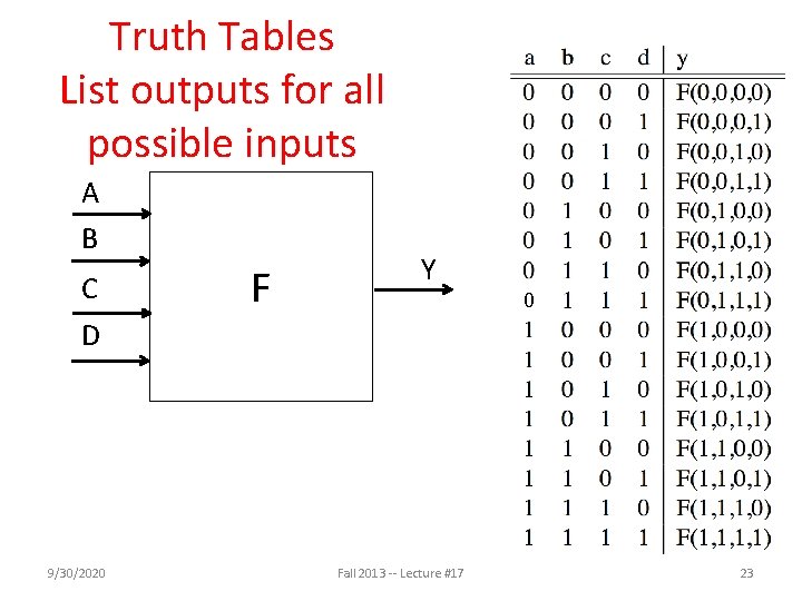
Truth Tables List outputs for all possible inputs A B C D 9/30/2020 F Y Fall 2013 -- Lecture #17 0 23

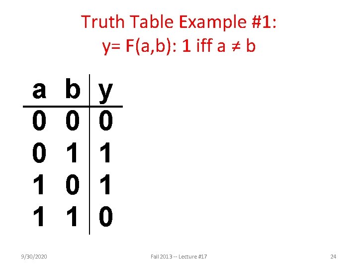
Truth Table Example #1: y= F(a, b): 1 iff a ≠ b a 0 0 1 1 b 0 1 y 0 1 1 0 Y=AB + AB Y=A + B XOR 9/30/2020 Fall 2013 -- Lecture #17 24

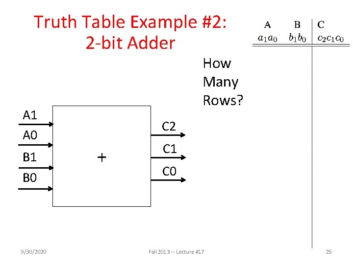
Truth Table Example #2: 2 -bit Adder How Many Rows? A 1 A 0 B 1 B 0 9/30/2020 C 2 + C 1 C 0 Fall 2013 -- Lecture #17 25

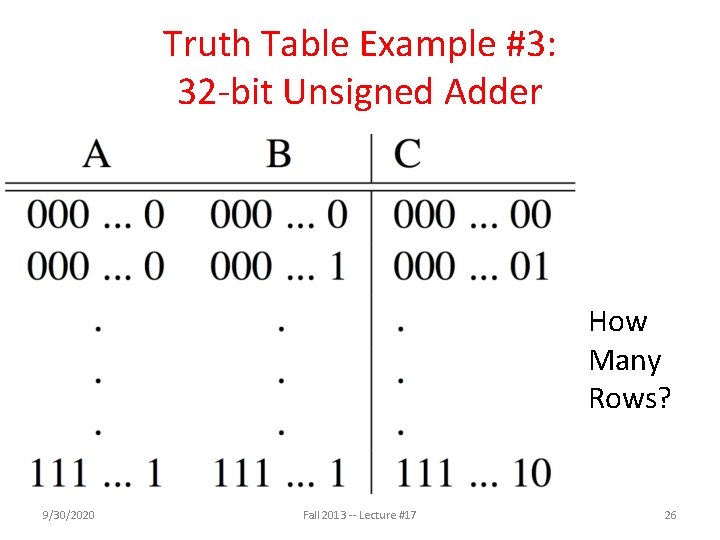
Truth Table Example #3: 32 -bit Unsigned Adder How Many Rows? 9/30/2020 Fall 2013 -- Lecture #17 26

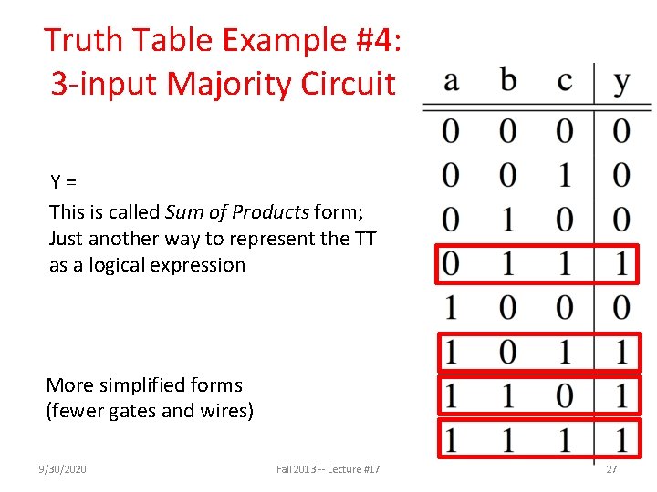
Truth Table Example #4: 3 -input Majority Circuit Y=ABC + ABC This is called Sum of Products form; Just another way to represent the TT as a logical expression Y = B C + A (B C + B C) Y = B C + A (B + C) More simplified forms (fewer gates and wires) 9/30/2020 Fall 2013 -- Lecture #17 27

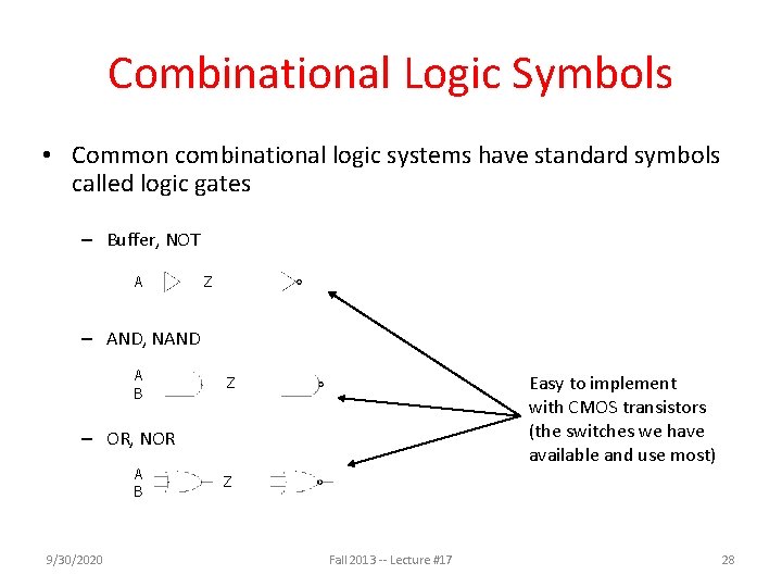
Combinational Logic Symbols • Common combinational logic systems have standard symbols called logic gates – Buffer, NOT A Z – AND, NAND A B Easy to implement with CMOS transistors (the switches we have available and use most) Z – OR, NOR A B 9/30/2020 Z Fall 2013 -- Lecture #17 28

Agenda • • • Switching Networks, Transistors Gates and Truth Tables for Circuits Boolean Algebra Logisim if there is time State Machines And in Conclusion, … 9/30/2020 Fall 2013 -- Lecture #17 29

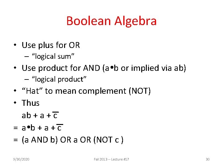
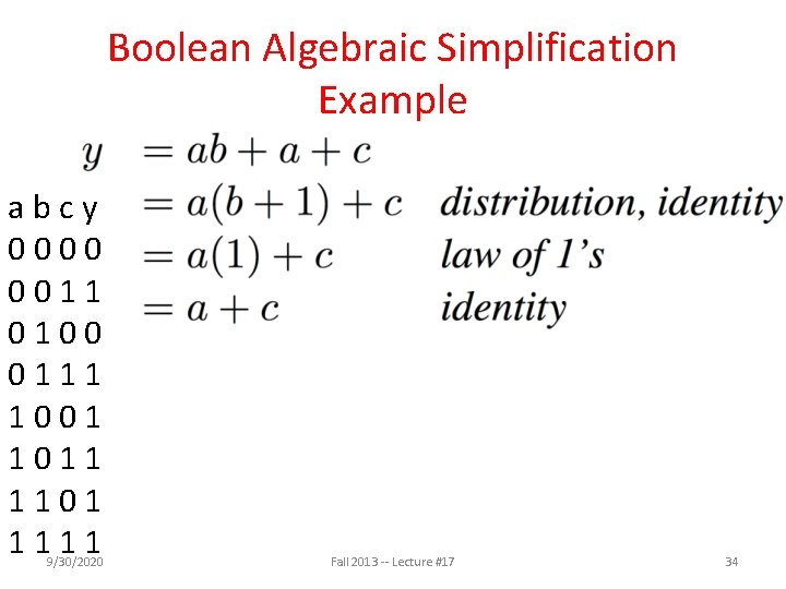
Boolean Algebra • Use plus for OR – “logical sum” • Use product for AND (a b or implied via ab) – “logical product” • “Hat” to mean complement (NOT) • Thus ab + a + c = a b + a + c = (a AND b) OR a OR (NOT c ) 9/30/2020 Fall 2013 -- Lecture #17 30

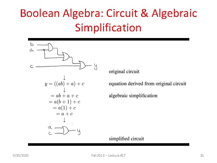
Boolean Algebra: Circuit & Algebraic Simplification 9/30/2020 Fall 2013 -- Lecture #17 31

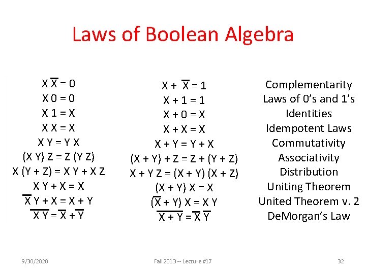
Laws of Boolean Algebra XX=0 X 0=0 X 1=X XX=X XY=YX (X Y) Z = Z (Y Z) X (Y + Z) = X Y + X Z XY+X=X+Y XY=X+Y 9/30/2020 X+ X=1 X+1=1 X+0=X X+X=X X+Y=Y+X (X + Y) + Z = Z + (Y + Z) X + Y Z = (X + Y) (X + Z) (X + Y) X = X Y X+Y=XY Fall 2013 -- Lecture #17 Complementarity Laws of 0’s and 1’s Identities Idempotent Laws Commutativity Associativity Distribution Uniting Theorem United Theorem v. 2 De. Morgan’s Law 32

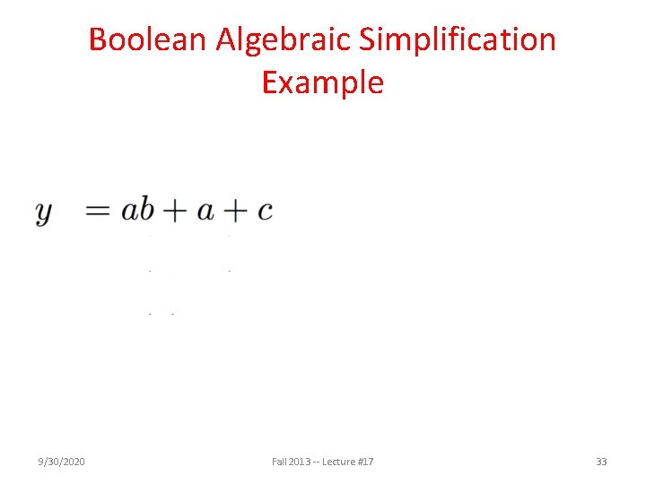
Boolean Algebraic Simplification Example 9/30/2020 Fall 2013 -- Lecture #17 33

Boolean Algebraic Simplification Example abcy 0000 0011 0100 0111 1001 1011 1101 1111 9/30/2020 Fall 2013 -- Lecture #17 34

Agenda • • • Switching Networks, Transistors Gates and Truth Tables for Circuits Boolean Algebra Logisim State Machines And in Conclusion, … 9/30/2020 Fall 2013 -- Lecture #17 35

Logisim • Free schematic capture/logic simulation program in Java – “A graphical tool for designing and simulating logic circuits” – Search and download version 2. 7. 1, online tutorial – ozark. hendrix. edu/~burch/logisim/ • Drawing interface based on toolbar – Color-coded wires aid in simulating and debugging a circuit – Wiring tool draws horizontal and vertical wires, automatically connecting to components and to other wires. • Circuit layouts used as "subcircuits" of other circuits, allowing hierarchical circuit design • Included circuit components: inputs and outputs, gates, multiplexers, arithmetic circuits, flip-flops, RAM memory 9/30/2020 Fall 2013 -- Lecture #17 36

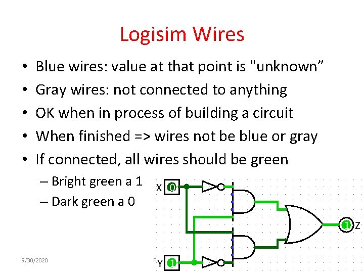
Logisim Wires • • • Blue wires: value at that point is "unknown” Gray wires: not connected to anything OK when in process of building a circuit When finished => wires not be blue or gray If connected, all wires should be green – Bright green a 1 – Dark green a 0 9/30/2020 Fall 2013 -- Lecture #17 37

Common Mistakes in Logisim • Connecting wires together • Using input for output • Connecting to edge without connecting to actual input – Unexpected direction of input 9/30/2020 Fall 2013 -- Lecture #17 38

Agenda • • • Switching Networks, Transistors Gates and Truth Tables for Circuits Boolean Algebra Logisim State Machines And in Conclusion, … 9/30/2020 Fall 2013 -- Lecture #17 39

Type of Circuits • Synchronous Digital Systems consist of two basic types of circuits: • Combinational Logic (CL) circuits – Output is a function of the inputs only, not the history of its execution – E. g. , circuits to add A, B (ALUs) – Last lecture was CL • Sequential Logic (SL) • • 9/30/2020 Circuits that “remember” or store information aka “State Elements” E. g. , memories and registers (Registers) Today’s lecture is SL Fall 2013 -- Lecture #17 40

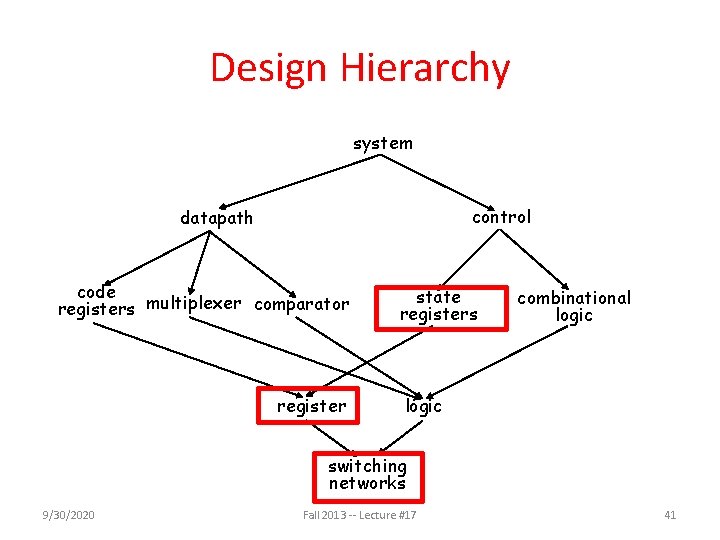
Design Hierarchy system control datapath code registers multiplexer comparator register state registers combinational logic switching networks 9/30/2020 Fall 2013 -- Lecture #17 41

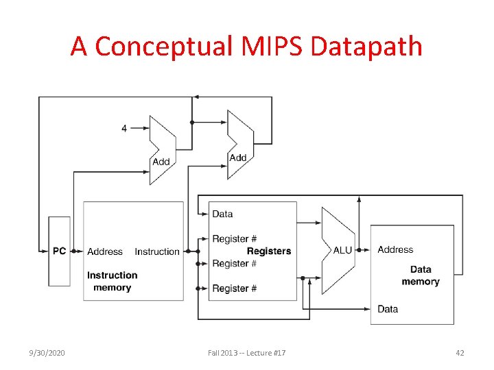
A Conceptual MIPS Datapath 9/30/2020 Fall 2013 -- Lecture #17 42

Uses for State Elements • Place to store values for later re-use: – Register files (like $1 -$31 on the MIPS) – Memory (caches, and main memory) • Help control flow of information between combinational logic blocks – State elements hold up the movement of information at input to combinational logic blocks to allow for orderly passage 9/30/2020 Fall 2013 -- Lecture #17 43

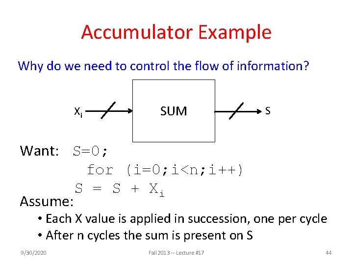
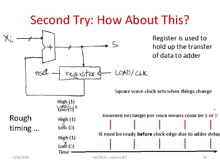
Accumulator Example Why do we need to control the flow of information? Xi SUM S Want: S=0; for (i=0; i<n; i++) S = S + Xi Assume: • Each X value is applied in succession, one per cycle • After n cycles the sum is present on S 9/30/2020 Fall 2013 -- Lecture #17 44

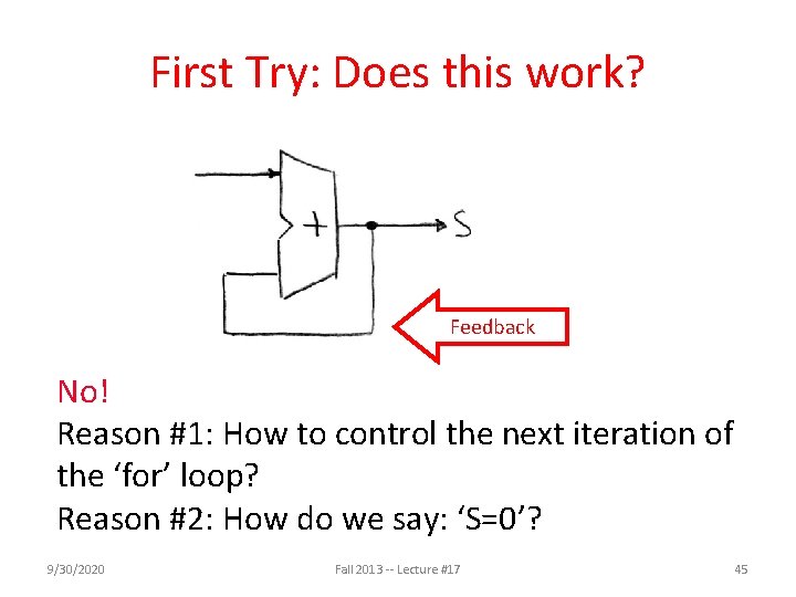
First Try: Does this work? Feedback No! Reason #1: How to control the next iteration of the ‘for’ loop? Reason #2: How do we say: ‘S=0’? 9/30/2020 Fall 2013 -- Lecture #17 45

Second Try: How About This? Register is used to hold up the transfer of data to adder Square wave clock sets when things change Rough timing … High (1) Low (0) High (1) 9/30/2020 Low (0) Time Rounded Rectangle per clock means could be 1 or 0 Xi must be ready before clock edge due to adder delay Fall 2013 -- Lecture #17 46

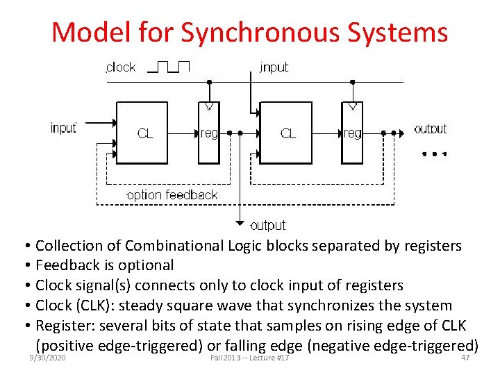
Model for Synchronous Systems • Collection of Combinational Logic blocks separated by registers • Feedback is optional • Clock signal(s) connects only to clock input of registers • Clock (CLK): steady square wave that synchronizes the system • Register: several bits of state that samples on rising edge of CLK (positive edge-triggered) or falling edge (negative edge-triggered) 9/30/2020 Fall 2013 -- Lecture #17 47

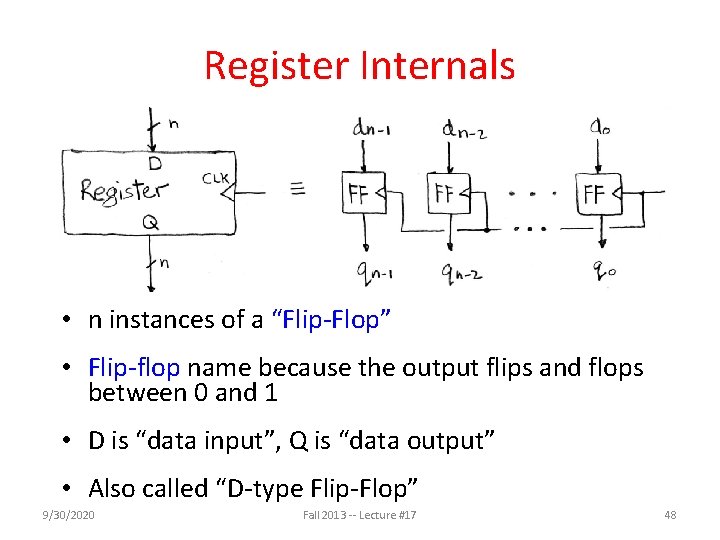
Register Internals • n instances of a “Flip-Flop” • Flip-flop name because the output flips and flops between 0 and 1 • D is “data input”, Q is “data output” • Also called “D-type Flip-Flop” 9/30/2020 Fall 2013 -- Lecture #17 48

Camera Analogy Timing Terms • Want to take a portrait – timing right before and after taking picture • Set up time – don’t move since about to take picture (open camera shutter) • Hold time – need to hold still after shutter opens until camera shutter closes • Time click to data – time from open shutter until can see image on output (viewfinder) 9/30/2020 Fall 2013 -- Lecture #17 49

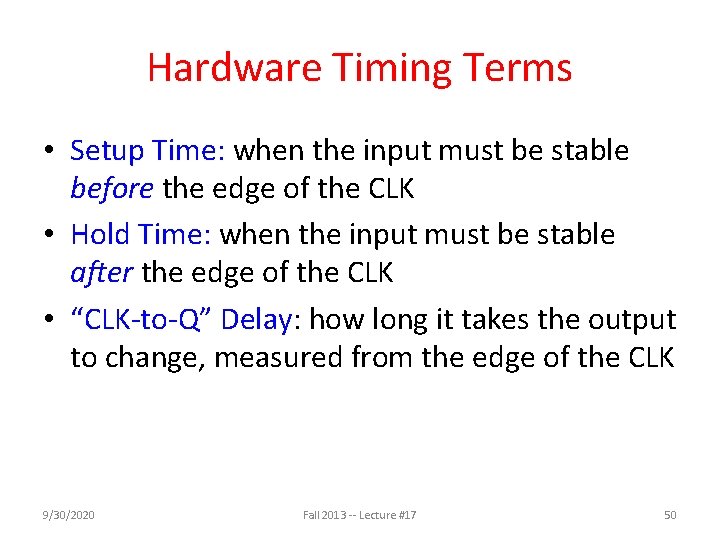
Hardware Timing Terms • Setup Time: when the input must be stable before the edge of the CLK • Hold Time: when the input must be stable after the edge of the CLK • “CLK-to-Q” Delay: how long it takes the output to change, measured from the edge of the CLK 9/30/2020 Fall 2013 -- Lecture #17 50

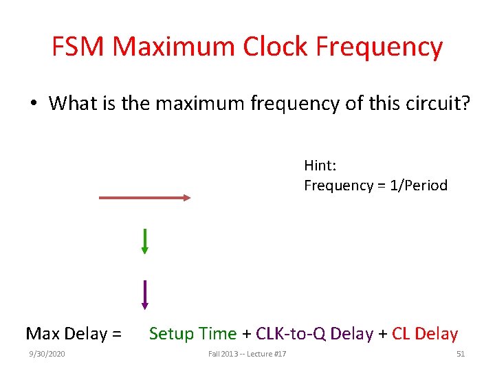
FSM Maximum Clock Frequency • What is the maximum frequency of this circuit? Hint: Frequency = 1/Period Max Delay = 9/30/2020 Setup Time + CLK-to-Q Delay + CL Delay Fall 2013 -- Lecture #17 51

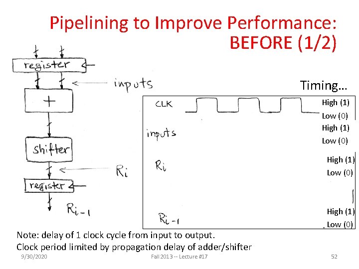
Pipelining to Improve Performance: BEFORE (1/2) Timing… High (1) Low (0) Note: delay of 1 clock cycle from input to output. Clock period limited by propagation delay of adder/shifter 9/30/2020 Fall 2013 -- Lecture #17 High (1) Low (0) 52

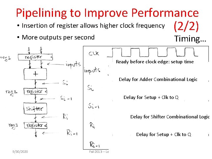
Pipelining to Improve Performance • Insertion of register allows higher clock frequency (2/2) Timing… • More outputs per second Ready before clock edge: setup time Delay for Adder Combinational Logic Delay for Setup + Clk to Q Delay for Shifter Combinational Logic Delay for Setup + Clk to Q 9/30/2020 Fall 2013 -- Lecture #17 53

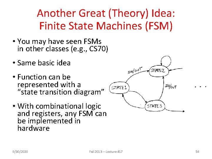
Another Great (Theory) Idea: Finite State Machines (FSM) • You may have seen FSMs in other classes (e. g. , CS 70) • Same basic idea • Function can be represented with a “state transition diagram” • With combinational logic and registers, any FSM can be implemented in hardware 9/30/2020 Fall 2013 -- Lecture #17 54

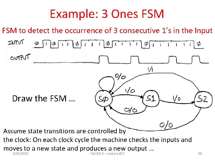
Example: 3 Ones FSM to detect the occurrence of 3 consecutive 1’s in the Input Draw the FSM … Assume state transitions are controlled by the clock: On each clock cycle the machine checks the inputs and moves to a new state and produces a new output … 9/30/2020 Fall 2013 -- Lecture #17 55

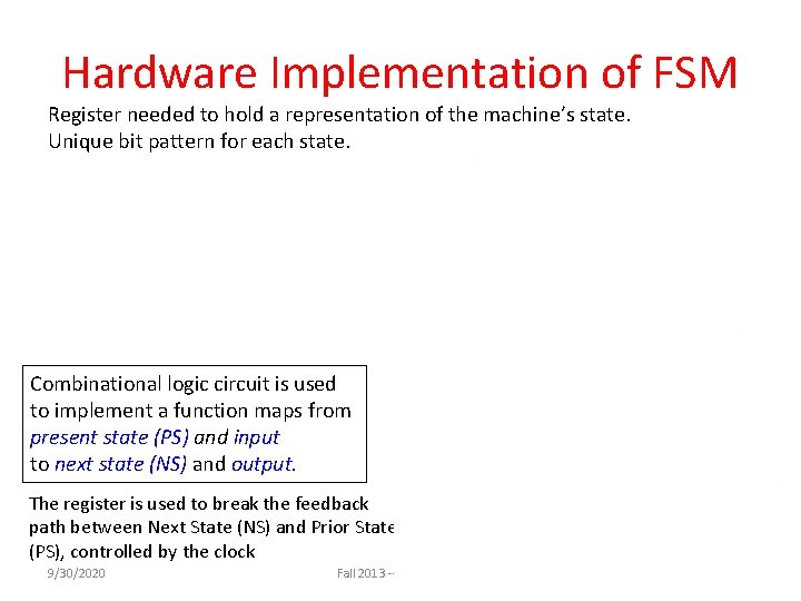
Hardware Implementation of FSM Register needed to hold a representation of the machine’s state. Unique bit pattern for each state. + Combinational logic circuit is used to implement a function maps from present state (PS) and input to next state (NS) and output. = The register is used to break the feedback path between Next State (NS) and Prior State (PS), controlled by the clock 9/30/2020 Fall 2013 -- Lecture #17 56

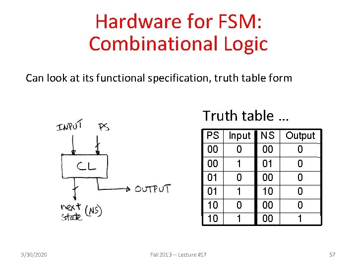
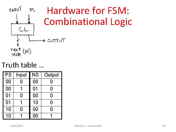
Hardware for FSM: Combinational Logic Can look at its functional specification, truth table form Truth table … PS Input 00 0 00 1 01 0 01 1 10 0 10 1 9/30/2020 Fall 2013 -- Lecture #17 NS 00 01 00 10 00 00 Output 0 0 0 1 57

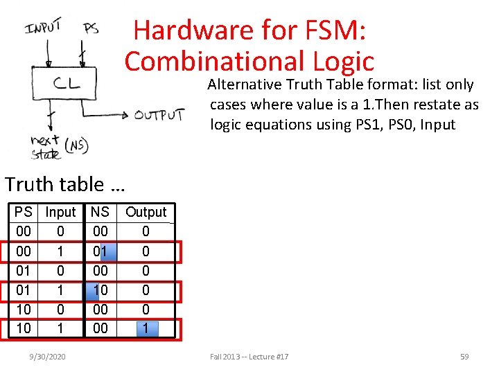
Hardware for FSM: Combinational Logic Truth table … PS Input 00 0 00 1 01 0 01 1 10 0 10 1 9/30/2020 NS 00 01 00 10 00 00 Output 0 0 0 1 Fall 2013 -- Lecture #17 58

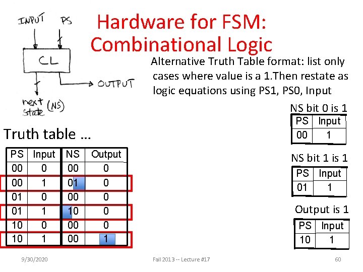
Hardware for FSM: Combinational Logic Alternative Truth Table format: list only cases where value is a 1. Then restate as logic equations using PS 1, PS 0, Input Truth table … PS Input 00 0 00 1 01 0 01 1 10 0 10 1 9/30/2020 NS 00 01 00 10 00 00 Output 0 0 0 1 Fall 2013 -- Lecture #17 59

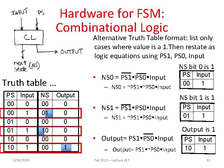
Hardware for FSM: Combinational Logic Alternative Truth Table format: list only cases where value is a 1. Then restate as logic equations using PS 1, PS 0, Input NS bit 0 is 1 PS Input 00 1 Truth table … PS Input 00 0 00 1 01 0 01 1 10 0 10 1 9/30/2020 NS 00 01 00 10 00 00 Output 0 0 0 1 NS bit 1 is 1 PS Input 01 1 Output is 1 PS Input 10 1 Fall 2013 -- Lecture #17 60

Hardware for FSM: Combinational Logic Truth table … PS Input 00 0 00 1 01 0 01 1 10 0 10 1 9/30/2020 NS 00 01 00 10 00 00 Output 0 0 0 1 Alternative Truth Table format: list only cases where value is a 1. Then restate as logic equations using PS 1, PS 0, Input NS bit 0 is 1 PS Input • NS 0 = PS 1 PS 0 Input – NS 0 = ~PS 1 ~PS 0 Input 00 1 NS bit 1 is 1 • NS 1 = PS 1 PS 0 Input – NS 1 = ~PS 1 PS 0 Input • Output= PS 1 PS 0 Input – Output= PS 1 ~PS 0 Input Fall 2013 -- Lecture #17 PS Input 01 1 Output is 1 PS Input 10 1 61

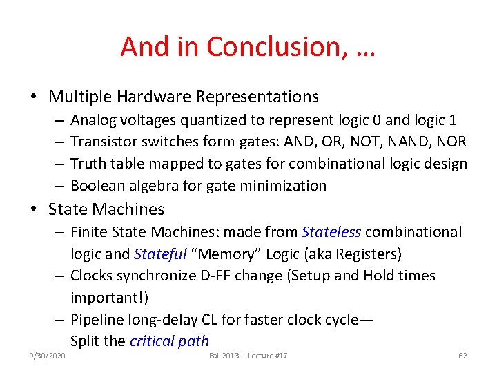
And in Conclusion, … • Multiple Hardware Representations – – Analog voltages quantized to represent logic 0 and logic 1 Transistor switches form gates: AND, OR, NOT, NAND, NOR Truth table mapped to gates for combinational logic design Boolean algebra for gate minimization • State Machines – Finite State Machines: made from Stateless combinational logic and Stateful “Memory” Logic (aka Registers) – Clocks synchronize D-FF change (Setup and Hold times important!) – Pipeline long-delay CL for faster clock cycle— Split the critical path 9/30/2020 Fall 2013 -- Lecture #17 62