CPD and other imaging technics for gas sensor
- Slides: 31

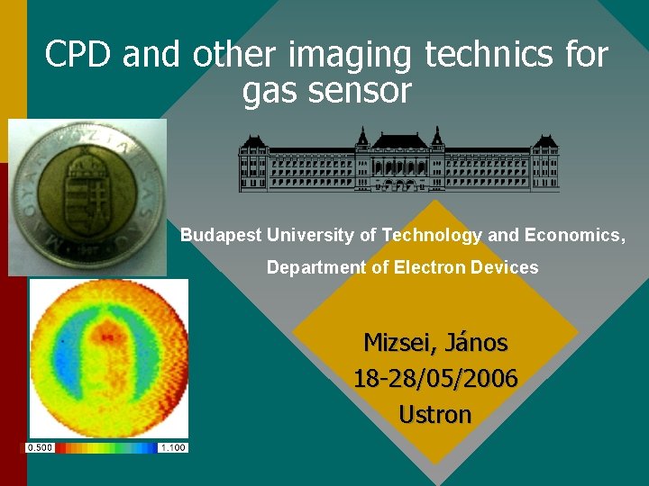
CPD and other imaging technics for gas sensor Budapest University of Technology and Economics, Department of Electron Devices Mizsei, János 18 -28/05/2006 Ustron

Outline • Introduction: potentials in general • Ideal (static) voltmeter. Do we really need contacts ? • What is it for ? Applications. . . • …extension of the application (x-y scanning, higher resolution, (Kelvin Force microscopy) etc. . . • Summary

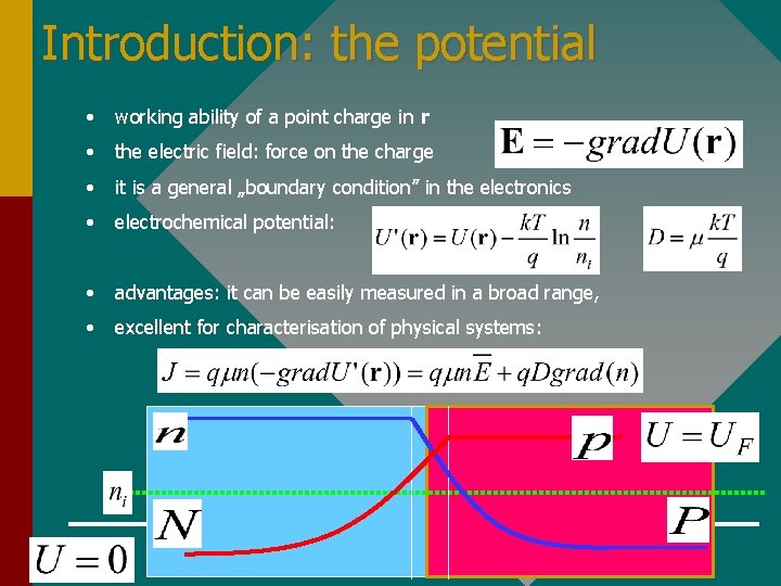
Introduction: the potential • working ability of a point charge in r • the electric field: force on the charge • it is a general „boundary condition” in the electronics • electrochemical potential: • advantages: it can be easily measured in a broad range, • excellent for characterisation of physical systems:

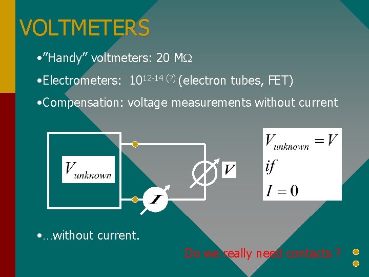
VOLTMETERS • ”Handy” voltmeters: 20 MW • Electrometers: 1012 -14 (? ) (electron tubes, FET) • Compensation: voltage measurements without current • …without current. Do we really need contacts ?

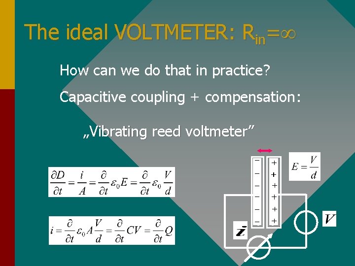
The ideal VOLTMETER: Rin=¥ How can we do that in practice? Capacitive coupling + compensation: „Vibrating reed voltmeter”

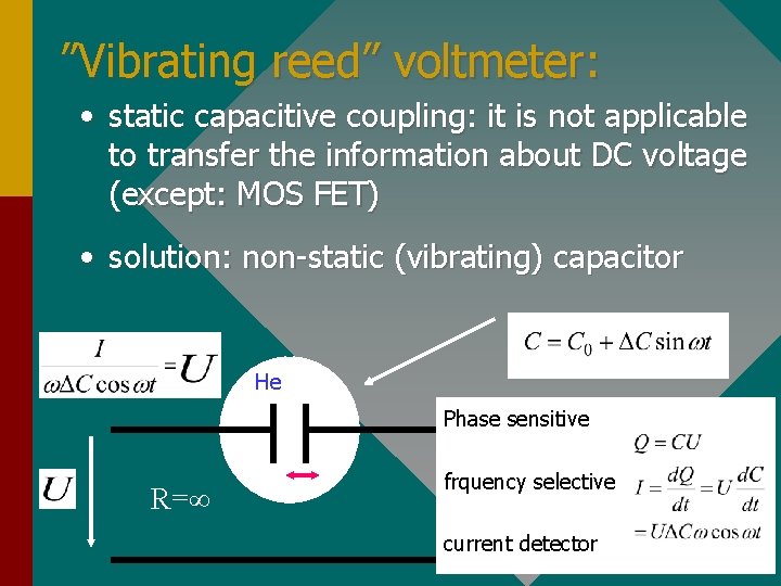
”Vibrating reed” voltmeter: • static capacitive coupling: it is not applicable to transfer the information about DC voltage (except: MOS FET) • solution: non-static (vibrating) capacitor He Phase sensitive R=¥ frquency selective current detector

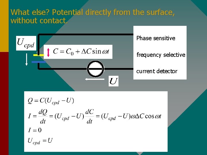
What else? Potential directly from the surface, without contact. Phase sensitive frequency selective current detector

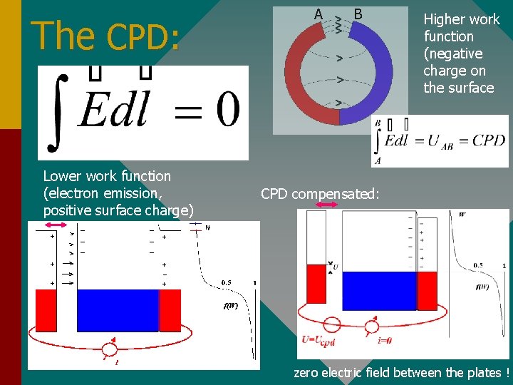
The CPD: Lower work function (electron emission, positive surface charge) A B Higher work function (negative charge on the surface CPD compensated: zero electric field between the plates !

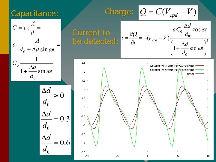
Capacitance: Charge: Current to be detected:

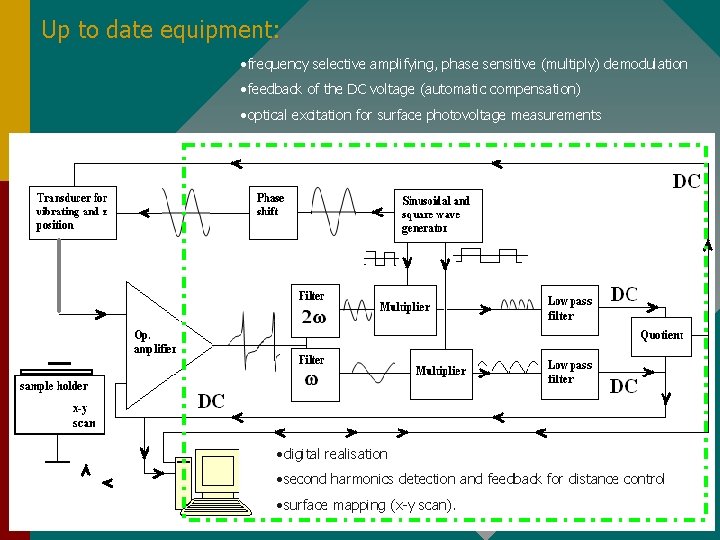
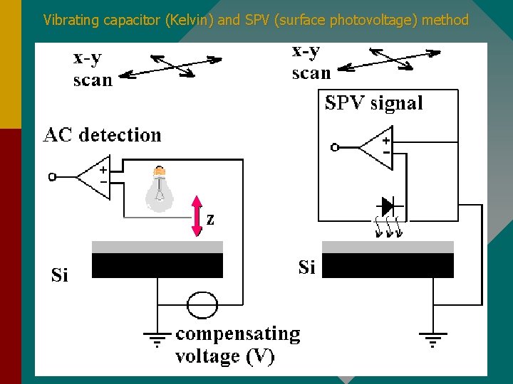
Up to date equipment: • frequency selective amplifying, phase sensitive (multiply) demodulation • feedback of the DC voltage (automatic compensation) • optical excitation for surface photovoltage measurements • digital realisation • second harmonics detection and feedback for distance control • surface mapping (x-y scan).

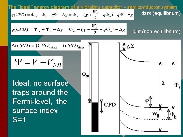
The “ideal” energy diagram of a vibrating capacitor - semiconductor system dark (equilibrium) light (non-equilibrium) Ideal: no surface traps around the Fermi-level, the surface index S=1

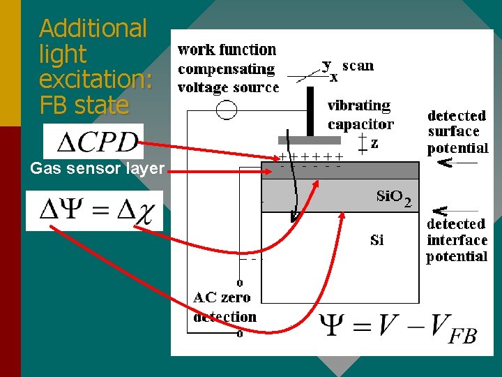
Additional light excitation: FB state Gas sensor layer

Vibrating capacitor (Kelvin) and SPV (surface photovoltage) method

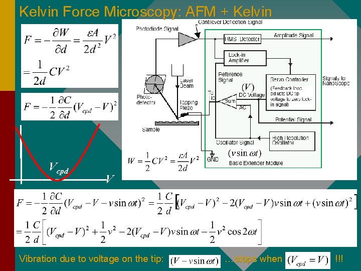
Kelvin Force Microscopy: AFM + Kelvin Vcpd V Vibration due to voltage on the tip: …stops when !!!

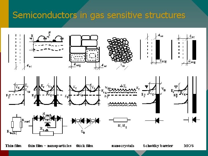
Semiconductors in gas sensitive structures

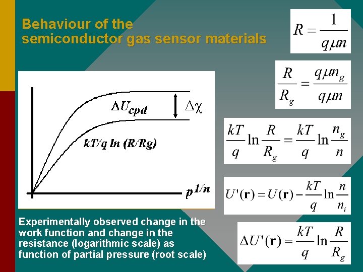
Behaviour of the semiconductor gas sensor materials Dc Experimentally observed change in the work function and change in the resistance (logarithmic scale) as function of partial pressure (root scale)

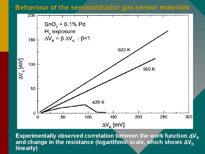
Behaviour of the semiconductor gas sensor materials Experimentally observed correlation between the work function DVK and change in the resistance (logarithmic scale, which shows DVR linearly)

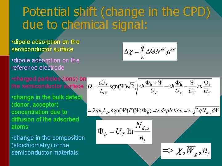
Potential shift (change in the CPD) due to chemical signal: • dipole adsorption on the semiconductor surface • dipole adsorption on the reference electrode • charged particles (ions) on the semiconductor surface • change in the bulk defect (donor, acceptor) concentration due to diffusion of the adsorbed atoms • change in the composition (stoichiometry) of the semiconductor materials

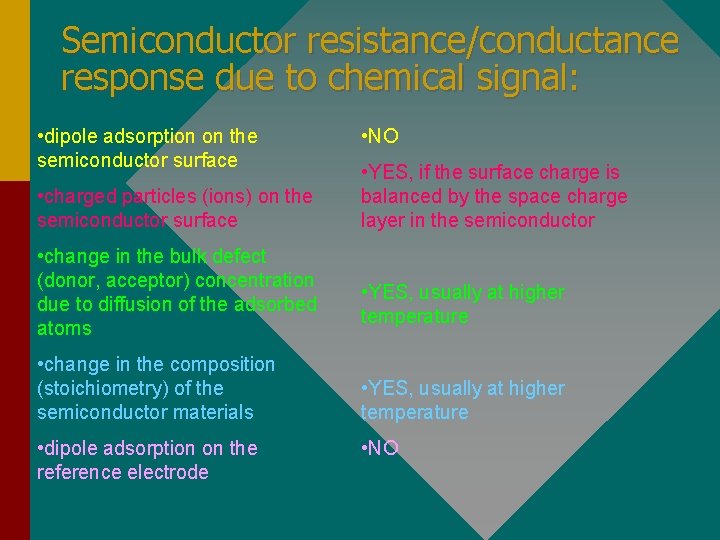
Semiconductor resistance/conductance response due to chemical signal: • dipole adsorption on the semiconductor surface • charged particles (ions) on the semiconductor surface • change in the bulk defect (donor, acceptor) concentration due to diffusion of the adsorbed atoms • change in the composition (stoichiometry) of the semiconductor materials • dipole adsorption on the reference electrode • NO • YES, if the surface charge is balanced by the space charge layer in the semiconductor • YES, usually at higher temperature • NO

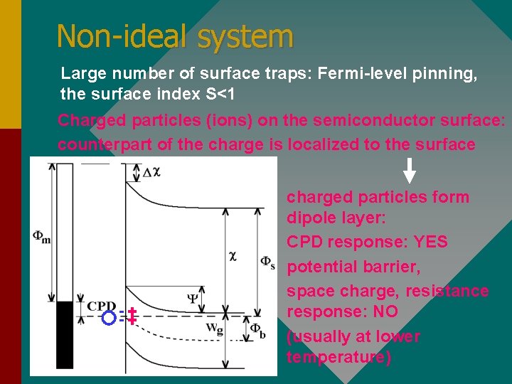
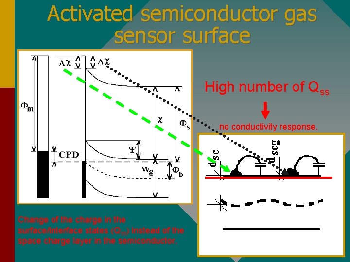
Non-ideal system Large number of surface traps: Fermi-level pinning, the surface index S<1 Charged particles (ions) on the semiconductor surface: counterpart of the charge is localized to the surface charged particles form dipole layer: CPD response: YES potential barrier, space charge, resistance response: NO (usually at lower temperature)

Activated semiconductor gas sensor surface High number of Qss no conductivity response. Change of the charge in the surface/interface states (Qss) instead of the space charge layer in the semiconductor.

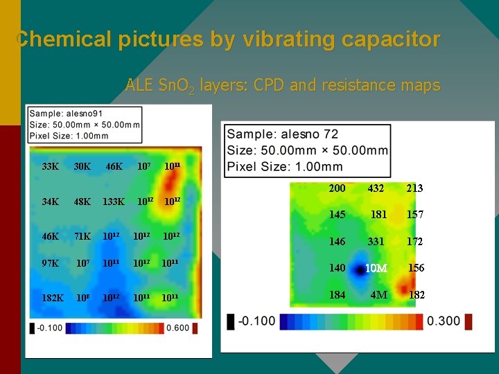
Chemical pictures by vibrating capacitor ALE Sn. O 2 layers: CPD and resistance maps 33 K 30 K 46 K 107 1011 34 K 48 K 133 K 1012 46 K 71 K 1012 97 K 107 1011 1012 1011 182 K 108 1012 1011 200 432 213 145 181 157 146 331 172 140 10 M 156 184 4 M 182

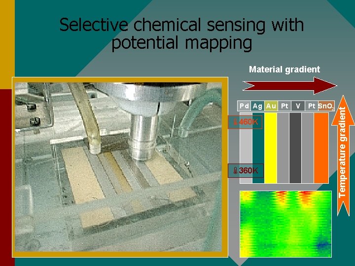
Selective chemical sensing with potential mapping Pd Ag Au Pt 460 K 360 K V Pt Sn. O 2 Temperature gradient Material gradient

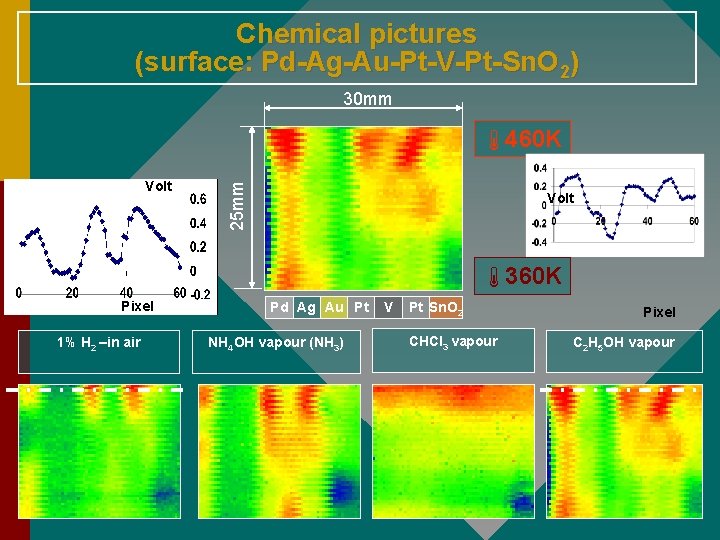
Chemical pictures (surface: Pd-Ag-Au-Pt-V-Pt-Sn. O 2) 30 mm 460 K Volt 25 mm C Volt 360 K Pixel 1% H 2 –in air Pd Ag Au Pt NH 4 OH vapour (NH 3) V Pt Sn. O 2 CHCl 3 vapour Pixel C 2 H 5 OH vapour

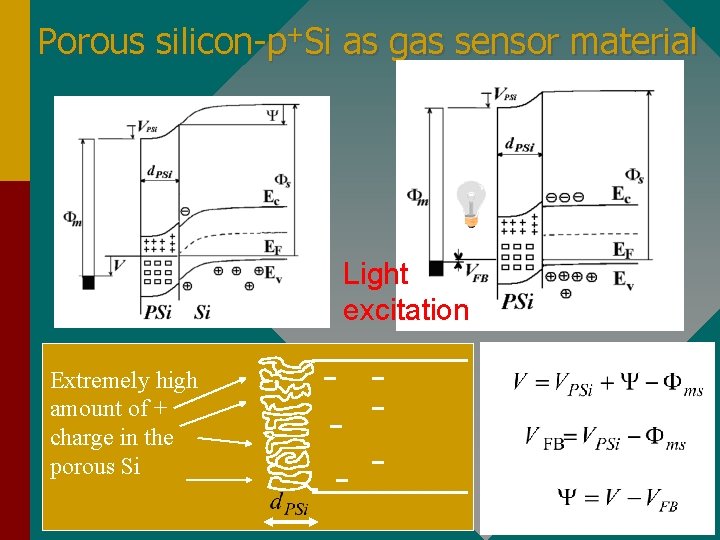
Porous silicon-p+Si as gas sensor material Light excitation Extremely high amount of + charge in the porous Si

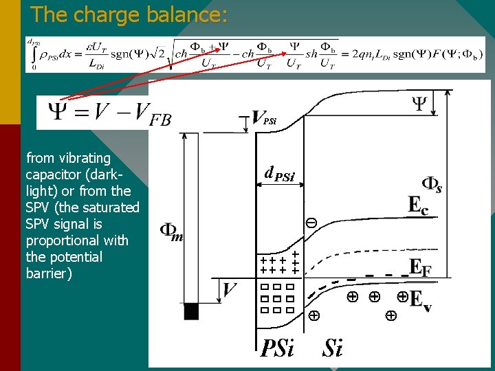
The charge balance: from vibrating capacitor (darklight) or from the SPV (the saturated SPV signal is proportional with the potential barrier)

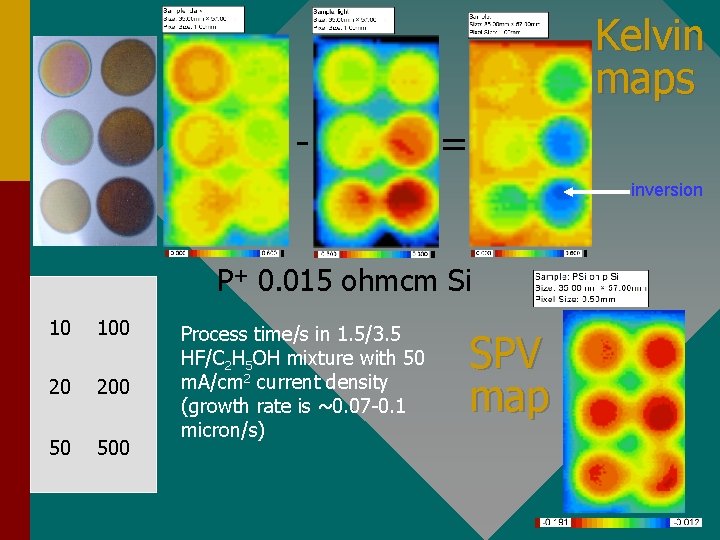
Kelvin maps - = inversion P+ 0. 015 ohmcm Si 10 100 20 200 50 500 Process time/s in 1. 5/3. 5 HF/C 2 H 5 OH mixture with 50 m. A/cm 2 current density (growth rate is ~0. 07 -0. 1 micron/s) SPV map

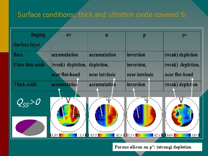
Surface conditions: thick and ultrathin oxide covered Si QSS>0 V Y Y V Porous silicon on p+: (strong) depletion

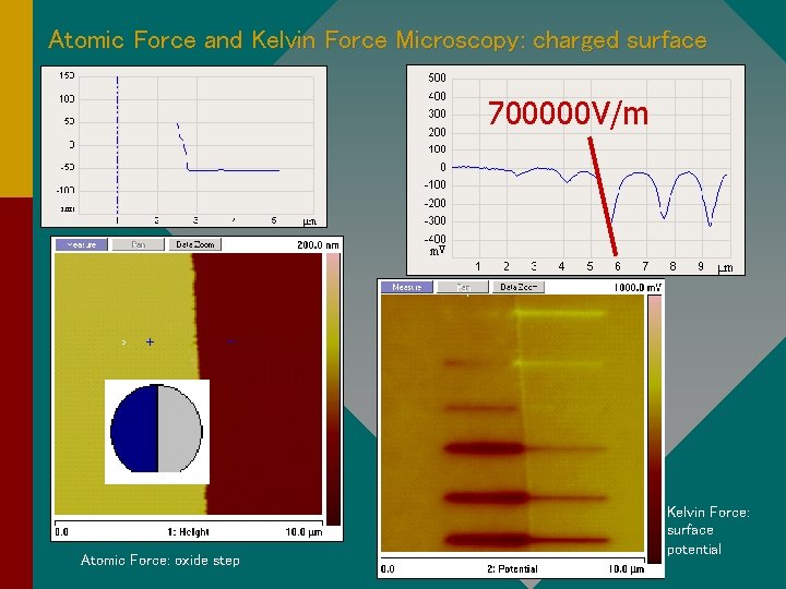
Atomic Force and Kelvin Force Microscopy: charged surface 700000 V/m 700000 V/ m Atomic Force: oxide step Kelvin Force: surface potential

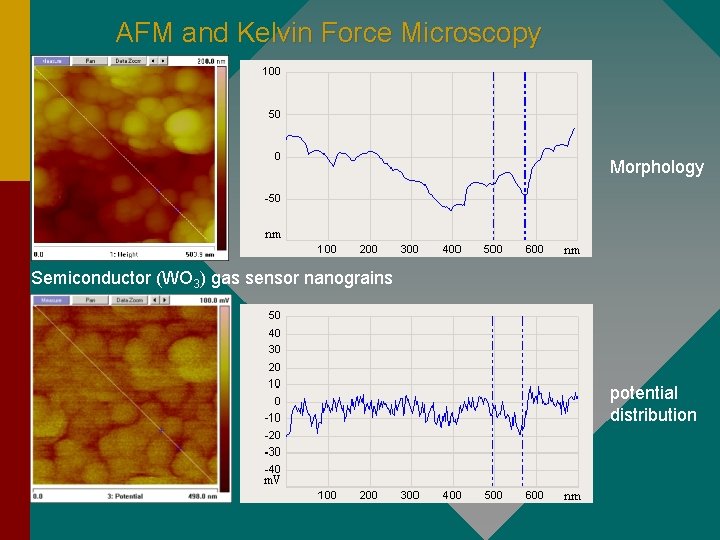
AFM and Kelvin Force Microscopy Morphology Semiconductor (WO 3) gas sensor nanograins potential distribution

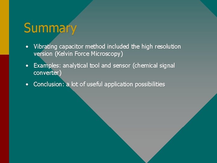
Summary • Vibrating capacitor method included the high resolution version (Kelvin Force Microscopy) • Examples: analytical tool and sensor (chemical signal converter) • Conclusion: a lot of useful application possibilities