Computer Organization CS 224 Fall 2012 Lesson 22
- Slides: 26

Computer Organization CS 224 Fall 2012 Lesson 22

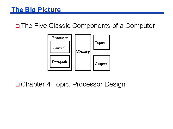
The Big Picture q The Five Classic Components of a Computer Processor Input Control Datapath q Chapter Memory Output 4 Topic: Processor Design

q CPU performance factors l Instruction count - Determined by ISA and compiler l CPI and Cycle time - Determined by CPU hardware q q We will examine two MIPS implementations l A simplified version l A more realistic pipelined version Simple subset, shows most aspects l Memory reference: lw, sw l Arithmetic/logical: add, sub, and, ori, slt l Control transfer: beq, j § 4. 1 Introduction

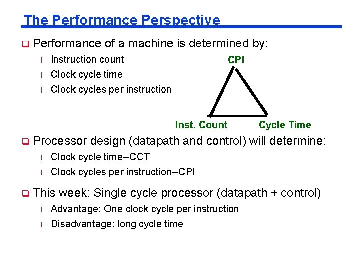
The Performance Perspective q Performance of a machine is determined by: l l l Instruction count Clock cycle time Clock cycles per instruction CPI Inst. Count q q Cycle Time Processor design (datapath and control) will determine: l Clock cycle time--CCT l Clock cycles per instruction--CPI This week: Single cycle processor (datapath + control) l l Advantage: One clock cycle per instruction Disadvantage: long cycle time

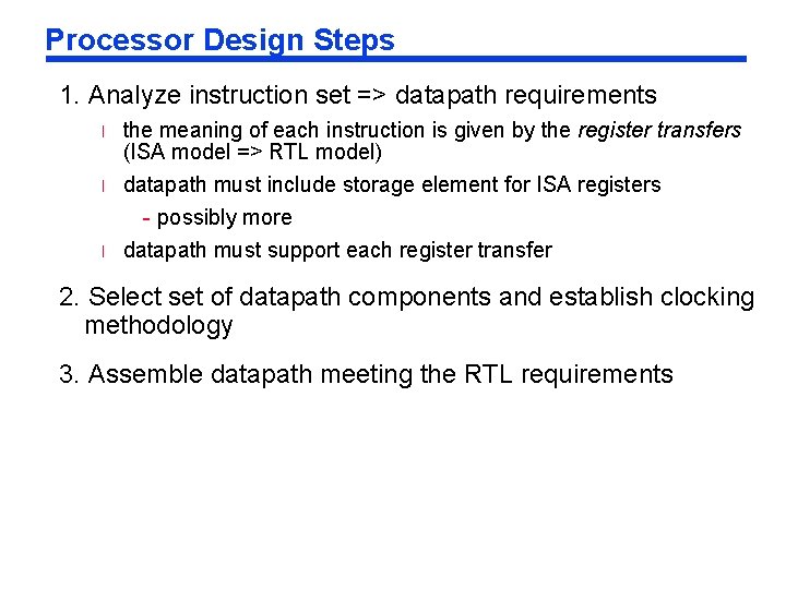
Processor Design Steps 1. Analyze instruction set => datapath requirements l the meaning of each instruction is given by the register transfers (ISA model => RTL model) datapath must include storage element for ISA registers l - possibly more datapath must support each register transfer l 2. Select set of datapath components and establish clocking methodology 3. Assemble datapath meeting the RTL requirements

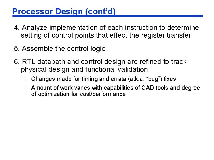
Processor Design (cont’d) 4. Analyze implementation of each instruction to determine setting of control points that effect the register transfer. 5. Assemble the control logic 6. RTL datapath and control design are refined to track physical design and functional validation l Changes made for timing and errata (a. k. a. “bug”) fixes l Amount of work varies with capabilities of CAD tools and degree of optimization for cost/performance

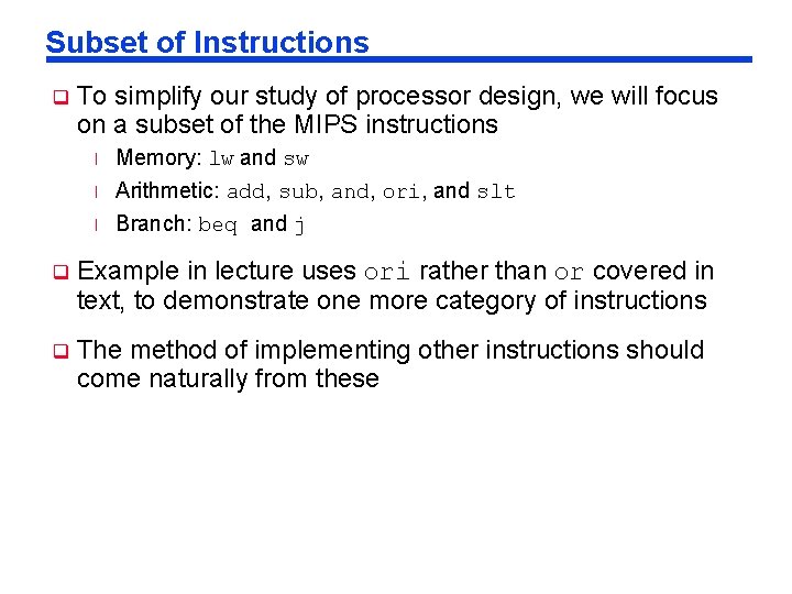
Subset of Instructions q To simplify our study of processor design, we will focus on a subset of the MIPS instructions l Memory: lw and sw Arithmetic: add, sub, and, ori, and slt l Branch: beq and j l q Example in lecture uses ori rather than or covered in text, to demonstrate one more category of instructions q The method of implementing other instructions should come naturally from these

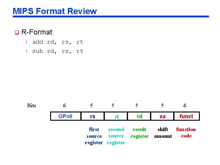
MIPS Format Review q R-Format l l add rd, rs, rt sub rd, rs, rt Bits 6 5 OP=0 rs 5 rt second first source register 5 5 6 rd sa function result shift code register amount

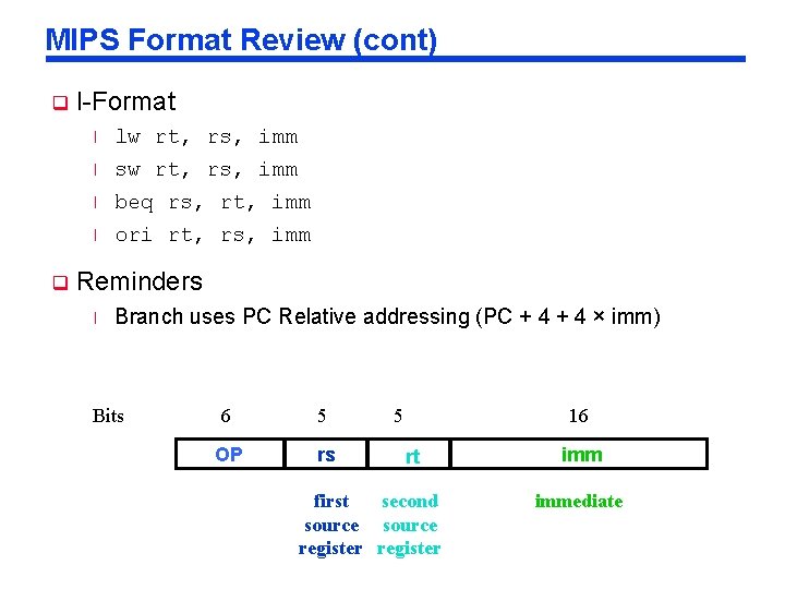
MIPS Format Review (cont) q I-Format l lw rt, rs, imm sw rt, rs, imm beq rs, rt, imm l ori rt, rs, imm l l q Reminders l Branch uses PC Relative addressing (PC + 4 × imm) Bits 6 5 OP rs 5 16 rt second first source register immediate

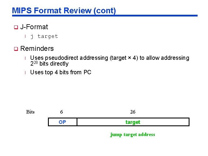
MIPS Format Review (cont) q J-Format l q j target Reminders l Uses pseudodirect addressing (target × 4) to allow addressing 228 bits directly l Uses top 4 bits from PC Bits 6 26 OP target jump target address

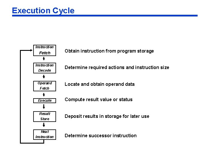
Execution Cycle Instruction Fetch Instruction Decode Operand Fetch Execute Result Store Next Instruction Obtain instruction from program storage Determine required actions and instruction size Locate and obtain operand data Compute result value or status Deposit results in storage for later use Determine successor instruction

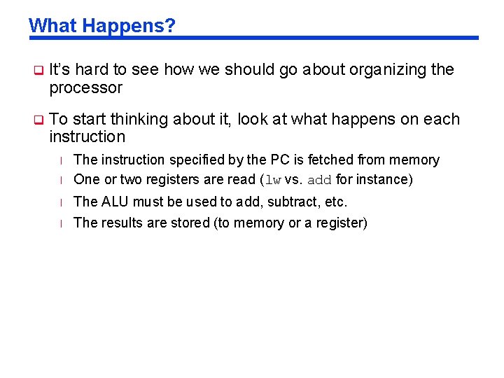
What Happens? q It’s hard to see how we should go about organizing the processor q To start thinking about it, look at what happens on each instruction l The instruction specified by the PC is fetched from memory One or two registers are read (lw vs. add for instance) l The ALU must be used to add, subtract, etc. l The results are stored (to memory or a register) l

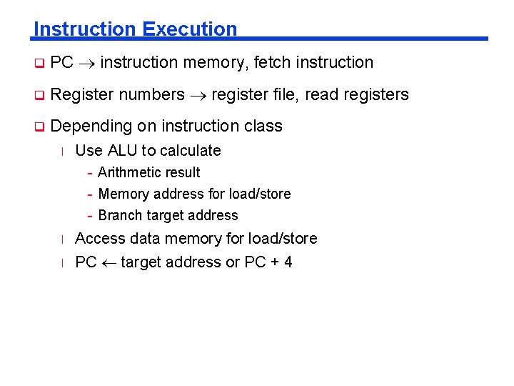
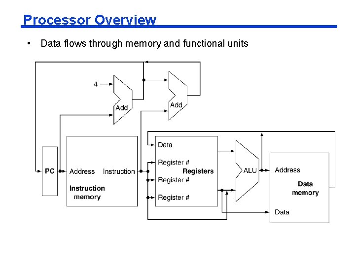
Instruction Execution q PC instruction memory, fetch instruction q Register numbers register file, read registers q Depending on instruction class l Use ALU to calculate - Arithmetic result - Memory address for load/store - Branch target address l l Access data memory for load/store PC target address or PC + 4

Processor Overview • Data flows through memory and functional units

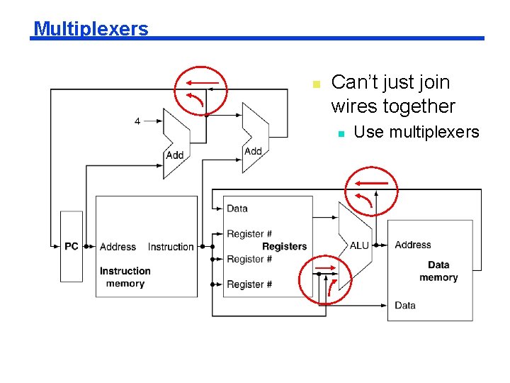
Multiplexers n Can’t just join wires together n Use multiplexers

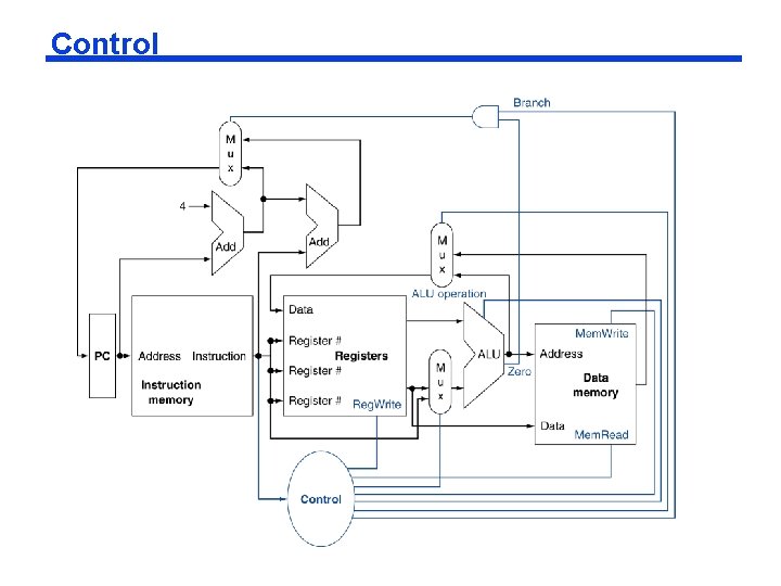
Control

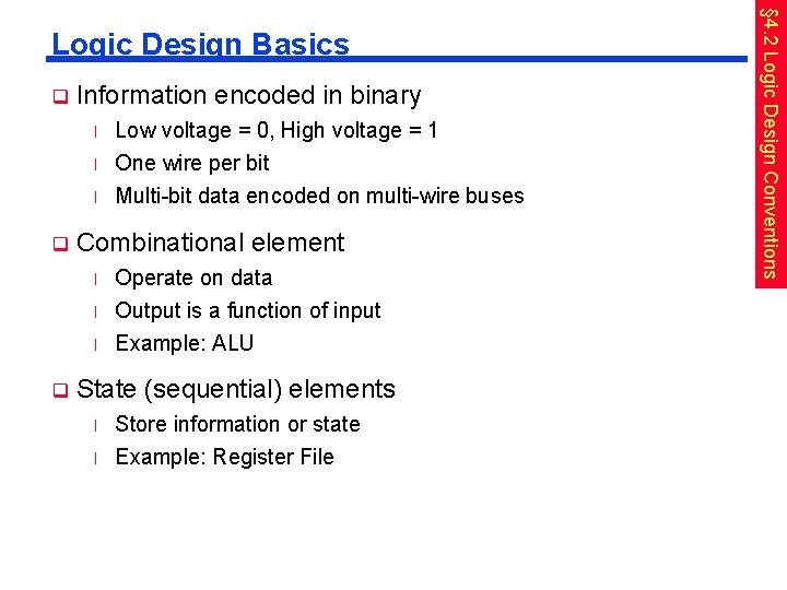
q Information encoded in binary l l l q q Low voltage = 0, High voltage = 1 One wire per bit Multi-bit data encoded on multi-wire buses Combinational element l Operate on data l Output is a function of input l Example: ALU State (sequential) elements l l Store information or state Example: Register File § 4. 2 Logic Design Conventions Logic Design Basics

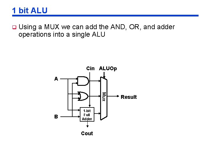
1 bit ALU q Using a MUX we can add the AND, OR, and adder operations into a single ALU Cin ALUOp A Mux B 1 -bit Full Adder Cout Result

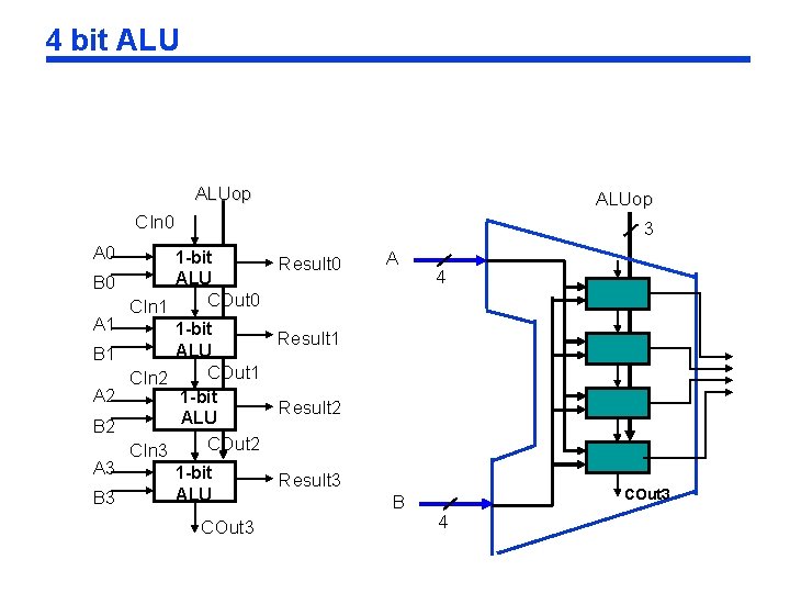
4 bit ALUop CIn 0 A 0 1 -bit ALU B 0 A 1 CIn 2 B 2 A 3 B 3 CIn 3 Result 0 A 4 COut 0 1 -bit ALU B 1 A 2 3 Result 1 COut 1 1 -bit ALU Result 2 COut 2 1 -bit ALU COut 3 Result 3 B COut 3 4

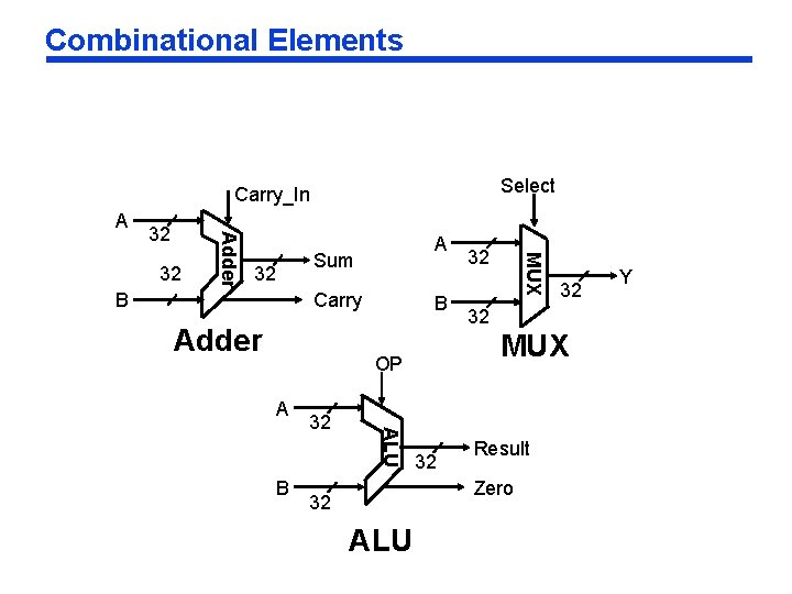
Combinational Elements Select Carry_In 32 32 B A Sum Carry Adder B ALU B 32 32 32 Result Zero 32 ALU 32 MUX OP A 32 MUX 32 Adder A Y

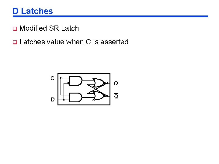
D Latches q Modified SR Latch q Latches value when C is asserted C D Q Q

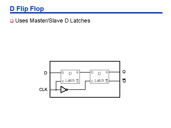
D Flip Flop q Uses Master/Slave D Latches D CLK D D Q Q C Latch Q Q

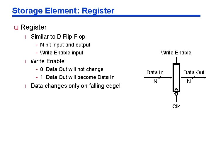
Storage Element: Register q Register l Similar to D Flip Flop - N bit input and output - Write Enable input l Write Enable - 0: Data Out will not change - 1: Data Out will become Data In l Write Enable Data changes only on falling edge! Data In Data Out N N Clk

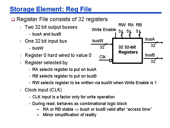
Storage Element: Reg File q Register File consists of 32 registers l Two 32 bit output busses - bus. A and bus. B l One 32 bit input bus - bus. W l Register 0 hard wired to value 0 l Register selected by RW RA RB Write Enable 5 5 5 bus. W 32 Clk 32 32 -bit Registers bus. A 32 bus. B 32 - RA selects register to put on bus. A - RB selects register to put on bus. B - RW selects register to be written via bus. W when Write Enable is 1 l Clock input (CLK) - CLK input is a factor only for write operation - During read, behaves as combinational logic block – RA or RB stable bus. A or bus. B valid after “access time” – Minor simplification of reality

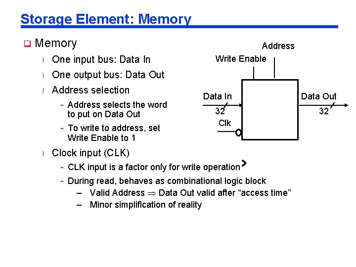
Storage Element: Memory q Memory l One input bus: Data In l One output bus: Data Out l Address selection - Address selects the word to put on Data Out - To write to address, set Write Enable to 1 l Address Write Enable Data In 32 Clk Clock input (CLK) - CLK input is a factor only for write operation - During read, behaves as combinational logic block – Valid Address Data Out valid after “access time” – Minor simplification of reality Data Out 32

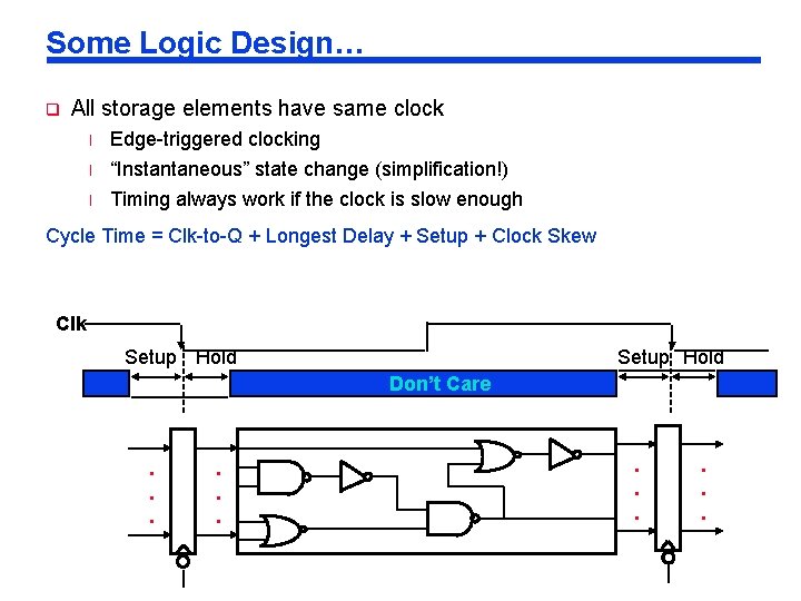
Some Logic Design… q All storage elements have same clock l l l Edge-triggered clocking “Instantaneous” state change (simplification!) Timing always work if the clock is slow enough Cycle Time = Clk-to-Q + Longest Delay + Setup + Clock Skew Clk Setup Hold Don’t Care . . .