CMOS RFIC Design for Direct Conversion Receivers Zhaofeng


- Slides: 34

CMOS RFIC Design for Direct Conversion Receivers Zhaofeng ZHANG

Outline of Presentation • Background Introduction • Design Issues and Solutions • A Direct Conversion Pager Receiver • Conclusion

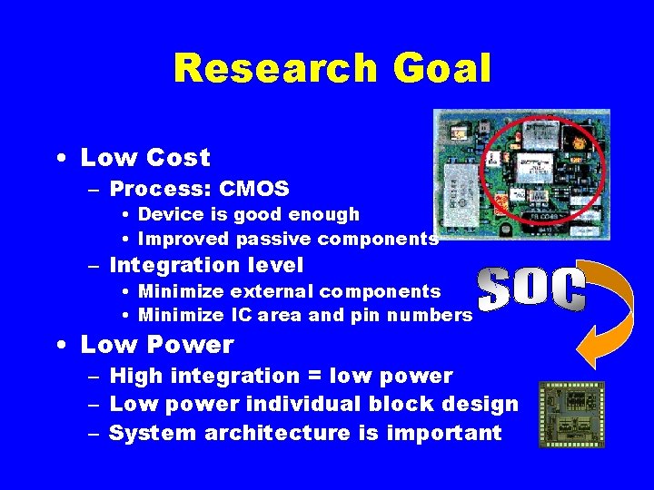
Research Goal • Low Cost – Process: CMOS • Device is good enough • Improved passive components – Integration level • Minimize external components • Minimize IC area and pin numbers • Low Power – High integration = low power – Low power individual block design – System architecture is important

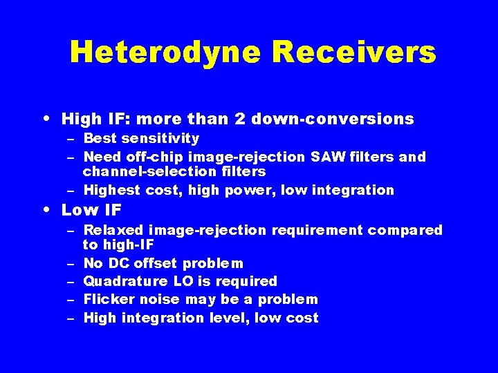
Heterodyne Receivers • High IF: more than 2 down-conversions – Best sensitivity – Need off-chip image-rejection SAW filters and channel-selection filters – Highest cost, high power, low integration • Low IF – Relaxed image-rejection requirement compared to high-IF – No DC offset problem – Quadrature LO is required – Flicker noise may be a problem – High integration level, low cost

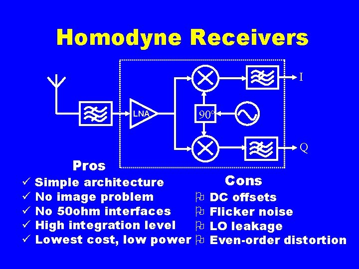
Homodyne Receivers I LNA 90º Q Pros ü ü ü Simple architecture No image problem No 50 ohm interfaces High integration level Lowest cost, low power Cons O O DC offsets Flicker noise LO leakage Even-order distortion

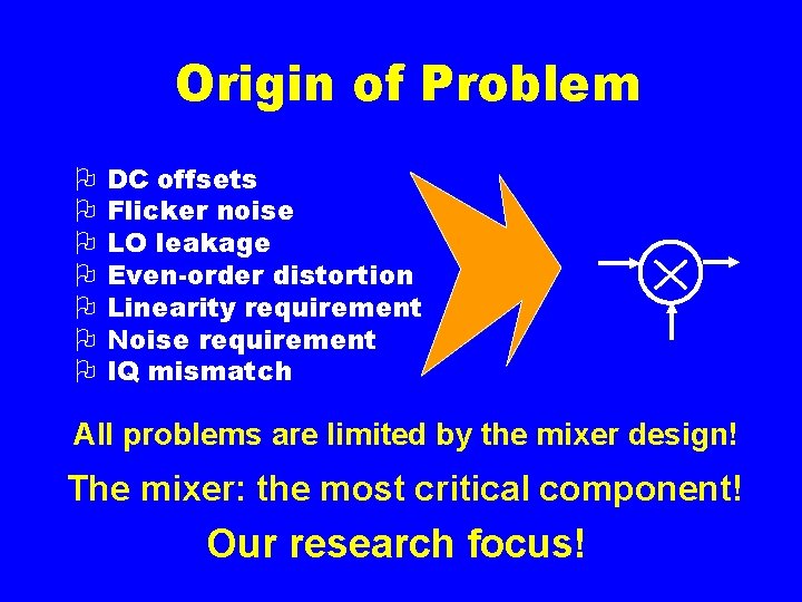
Origin of Problem O O O O DC offsets Flicker noise LO leakage Even-order distortion Linearity requirement Noise requirement IQ mismatch All problems are limited by the mixer design! The mixer: the most critical component! Our research focus!

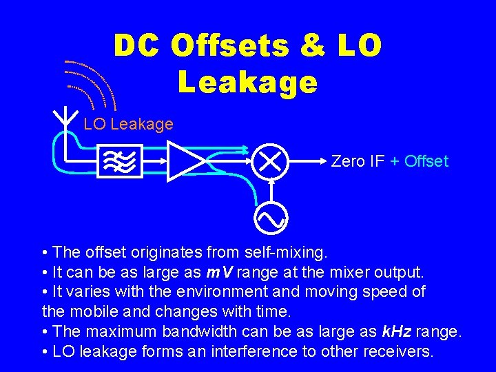
DC Offsets & LO Leakage Zero IF + Offset • The offset originates from self-mixing. • It can be as large as m. V range at the mixer output. • It varies with the environment and moving speed of the mobile and changes with time. • The maximum bandwidth can be as large as k. Hz range. • LO leakage forms an interference to other receivers.

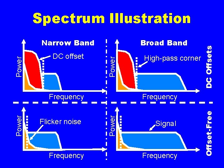
Flicker noise Frequency Power Frequency High-pass corner Signal Frequency Offset-Free DC offset Broad Band Power Narrow Band DC Offsets Spectrum Illustration

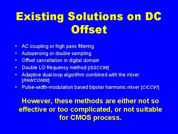
Existing Solutions on DC Offset • • • AC coupling or high pass filtering Autozeroing or double sampling Offset cancellation in digital domain Double LO frequency method [ISSCC 99] Adaptive dual-loop algorithm combined with the mixer [RAWCON 00] • Pulse-width-modulation based bipolar harmonic mixer [CICC 97] However, these methods are either not so effective or too complicated, or not suitable for CMOS process.

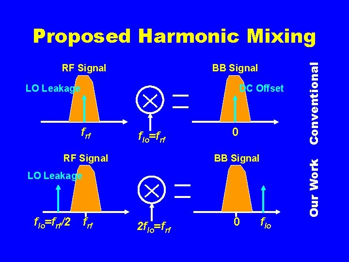
BB Signal LO Leakage DC Offset frf flo=frf RF Signal 0 BB Signal LO Leakage flo=frf/2 frf 2 flo=frf 0 flo Our Work RF Signal Conventional Proposed Harmonic Mixing

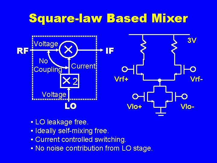
Square-law Based Mixer RF 3 V Voltage IF No Coupling Current 2 Vrf+ Vrf- Voltage LO Vlo+ • LO leakage free. • Ideally self-mixing free. • Current controlled switching. • No noise contribution from LO stage. Vlo-

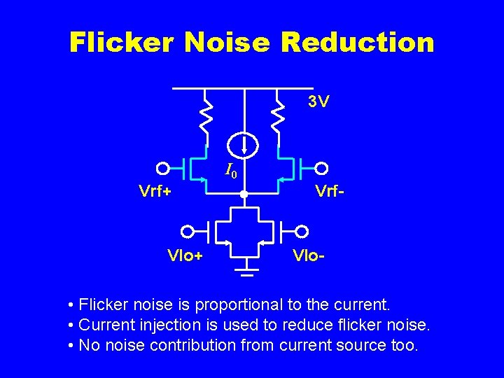
Flicker Noise Reduction 3 V I 0 Vrf+ Vlo+ Vrf- Vlo- • Flicker noise is proportional to the current. • Current injection is used to reduce flicker noise. • No noise contribution from current source too.

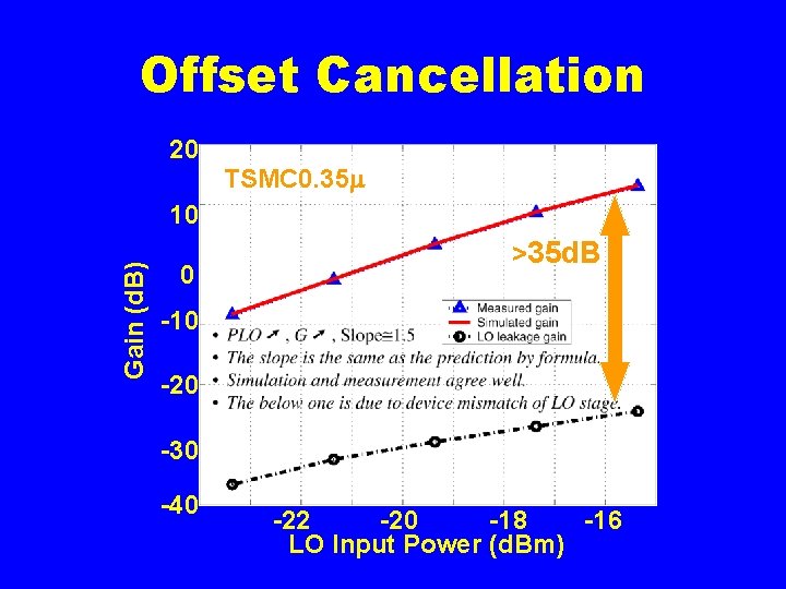
Offset Cancellation 20 TSMC 0. 35 Gain (d. B) 10 0 >35 d. B -10 -20 -30 -40 -22 -20 -18 -16 LO Input Power (d. Bm)

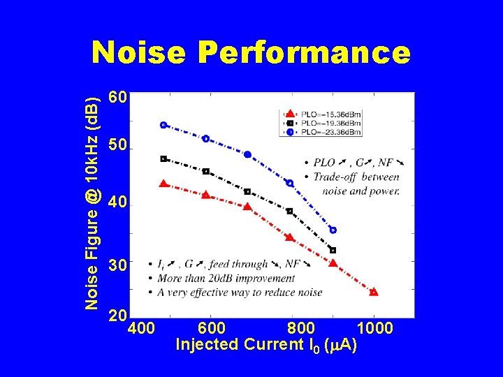
Noise Figure @ 10 k. Hz (d. B) Noise Performance 60 50 40 30 20 400 600 800 1000 Injected Current I 0 ( A)

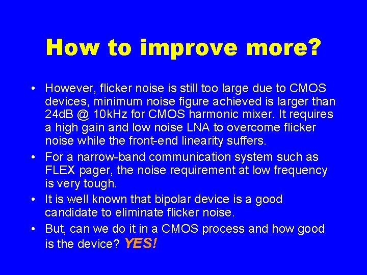
How to improve more? • However, flicker noise is still too large due to CMOS devices, minimum noise figure achieved is larger than 24 d. B @ 10 k. Hz for CMOS harmonic mixer. It requires a high gain and low noise LNA to overcome flicker noise while the front-end linearity suffers. • For a narrow-band communication system such as FLEX pager, the noise requirement at low frequency is very tough. • It is well known that bipolar device is a good candidate to eliminate flicker noise. • But, can we do it in a CMOS process and how good is the device? YES!

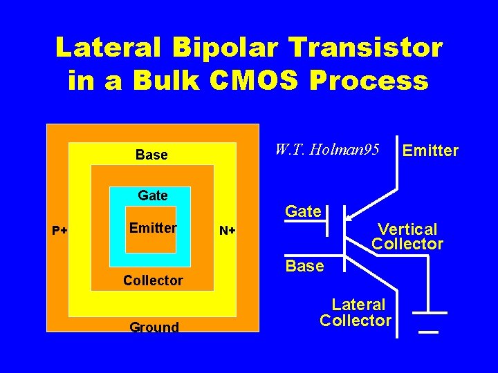
Lateral Bipolar Transistor in a Bulk CMOS Process W. T. Holman 95 Base Gate P+ Emitter Collector Ground Emitter Gate Vertical Collector N+ Base Lateral Collector

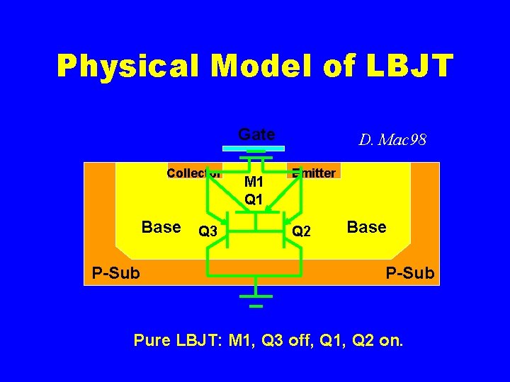
Physical Model of LBJT Gate Collector Base Q 3 P-Sub M 1 Q 1 D. Mac 98 Emitter Q 2 Base P-Sub Pure LBJT: M 1, Q 3 off, Q 1, Q 2 on.

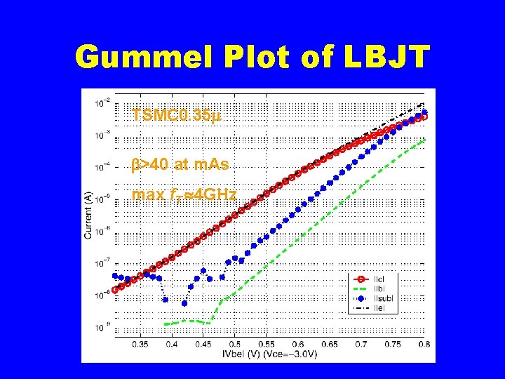
Gummel Plot of LBJT TSMC 0. 35 >40 at m. As max f. T 4 GHz

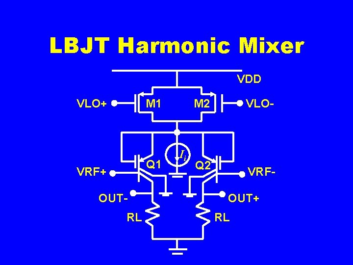
LBJT Harmonic Mixer VDD VLO+ M 1 Q 1 VRF+ OUTRL VLO- M 2 Ii Q 2 VRFOUT+ RL

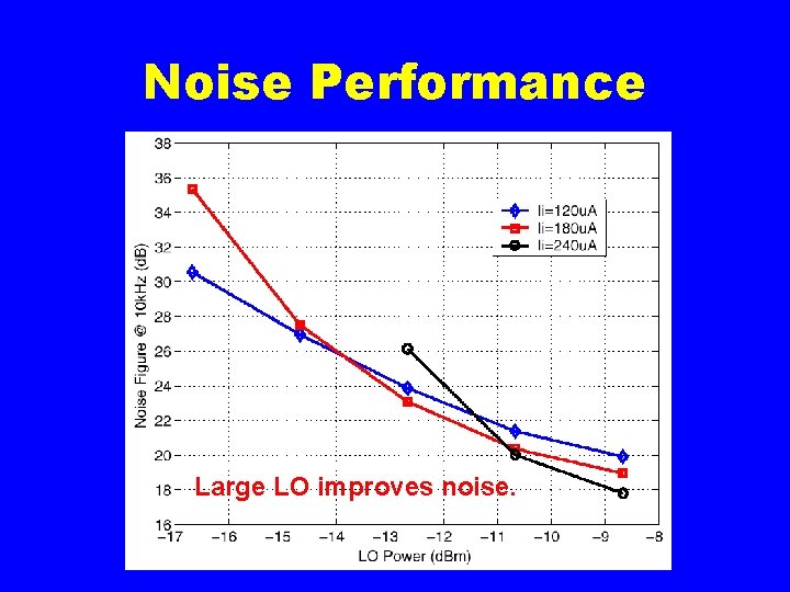
Noise Performance Large LO improves noise.

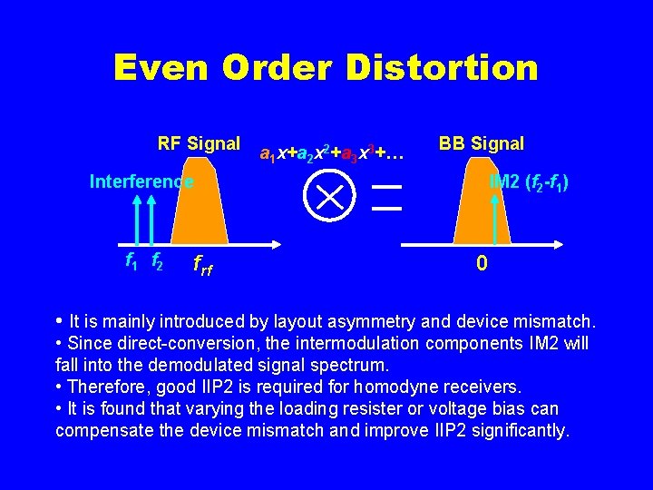
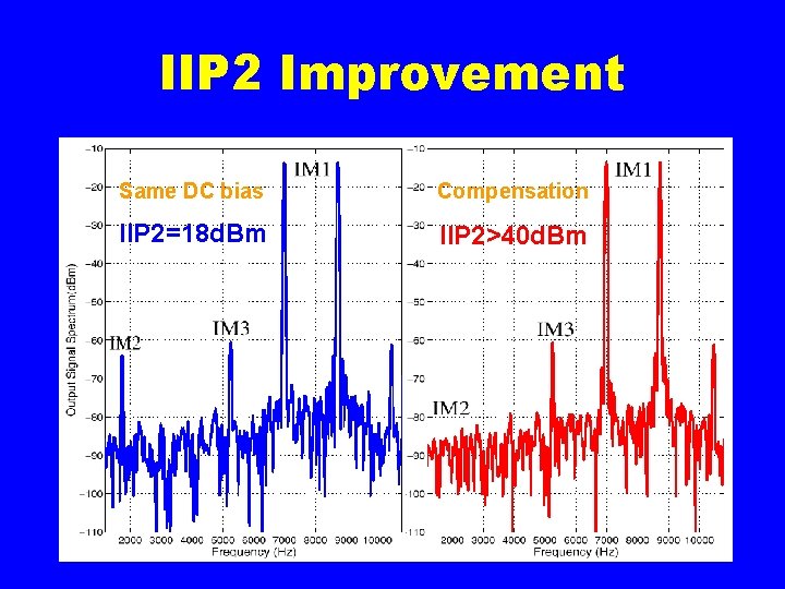
Even Order Distortion RF Signal a 1 x+a 2 x 2+a 3 x 3+… BB Signal IM 2 (f 2 -f 1) Interference f 1 f 2 frf 0 • It is mainly introduced by layout asymmetry and device mismatch. • Since direct-conversion, the intermodulation components IM 2 will fall into the demodulated signal spectrum. • Therefore, good IIP 2 is required for homodyne receivers. • It is found that varying the loading resister or voltage bias can compensate the device mismatch and improve IIP 2 significantly.

IIP 2 Improvement Same DC bias Compensation IIP 2=18 d. Bm IIP 2>40 d. Bm

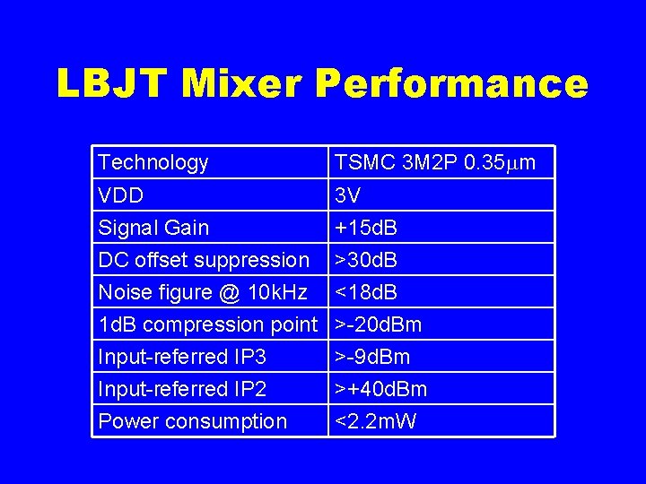
LBJT Mixer Performance Technology TSMC 3 M 2 P 0. 35 m VDD Signal Gain DC offset suppression 3 V +15 d. B >30 d. B Noise figure @ 10 k. Hz 1 d. B compression point Input-referred IP 3 Input-referred IP 2 Power consumption <18 d. B >-20 d. Bm >-9 d. Bm >+40 d. Bm <2. 2 m. W

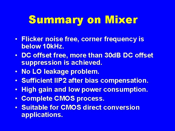
Summary on Mixer • Flicker noise free, corner frequency is below 10 k. Hz. • DC offset free, more than 30 d. B DC offset suppression is achieved. • No LO leakage problem. • Sufficient IIP 2 after bias compensation. • High gain and low power consumption. • Complete CMOS process. • Suitable for CMOS direct conversion applications.

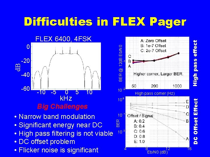
Difficulties in FLEX Pager BER @ 12 d. B Eb/N 0 0 -20 0 5 10 k. Hz Big Challenges • Narrow band modulation • Significant energy near DC • High pass filtering is not viable • DC offset problem • Flicker noise is significant 10 -2 High pass corner (Hz) 10 0 DC Offset Effect -10 -5 10 -1 BER d. B -1 -40 -60 High pass effect FLEX 6400, 4 FSK 10 -2 4 8 12 Eb/N 0 (d. B) 16

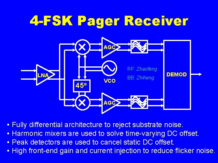
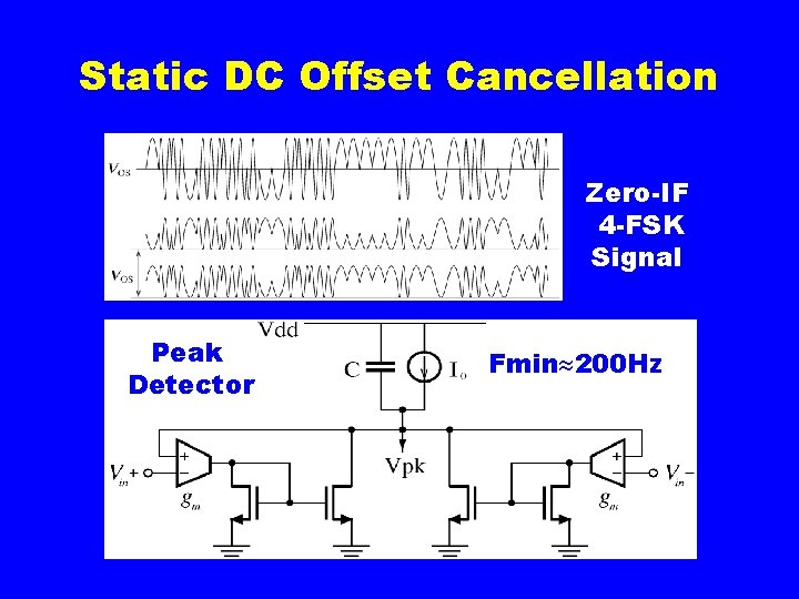
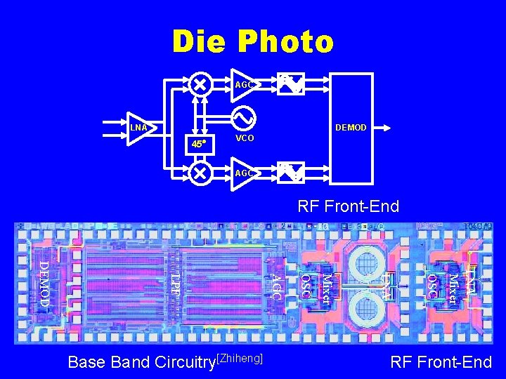
4 -FSK Pager Receiver AGC RF: Zhaofeng LNA 45 VCO BB: Zhiheng DEMOD AGC • Fully differential architecture to reject substrate noise. • Harmonic mixers are used to solve time-varying DC offset. • Peak detectors are used to cancel static DC offset. • High front-end gain and current injection to reduce flicker noise.

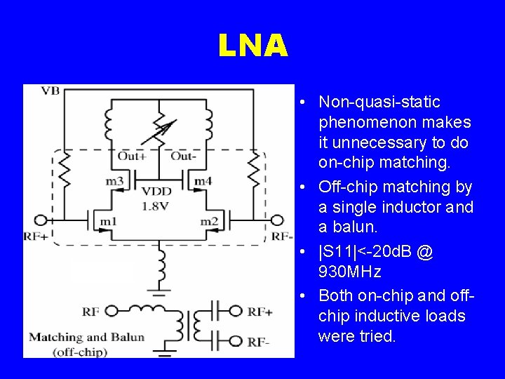
LNA • Non-quasi-static phenomenon makes it unnecessary to do on-chip matching. • Off-chip matching by a single inductor and a balun. • |S 11|<-20 d. B @ 930 MHz • Both on-chip and offchip inductive loads were tried.

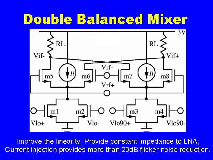
Double Balanced Mixer Improve the linearity; Provide constant impedance to LNA; Current injection provides more than 20 d. B flicker noise reduction.

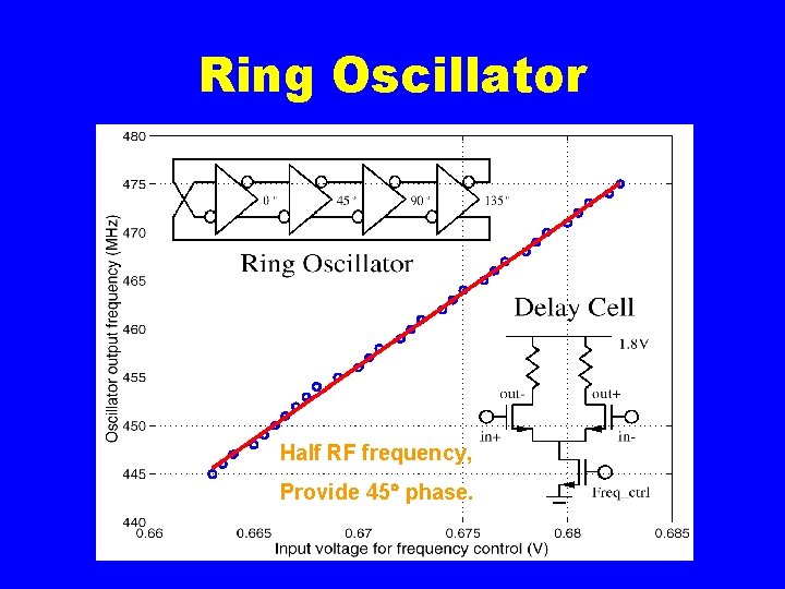
Ring Oscillator Half RF frequency, Provide 45 phase.

Static DC Offset Cancellation Zero-IF 4 -FSK Signal Peak Detector Fmin 200 Hz

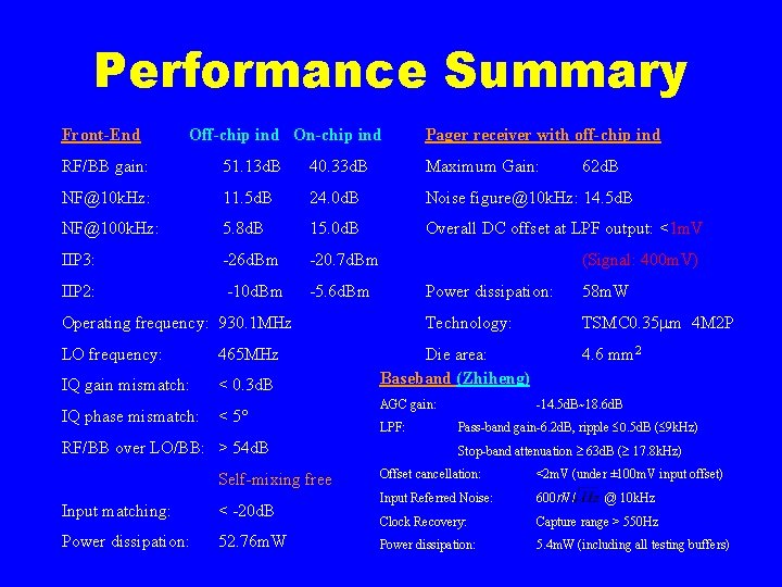
Performance Summary Front-End Off-chip ind On-chip ind Pager receiver with off-chip ind RF/BB gain: 51. 13 d. B 40. 33 d. B Maximum Gain: NF@10 k. Hz: 11. 5 d. B 24. 0 d. B Noise figure@10 k. Hz: 14. 5 d. B NF@100 k. Hz: 5. 8 d. B 15. 0 d. B Overall DC offset at LPF output: <1 m. V IIP 3: -26 d. Bm -20. 7 d. Bm IIP 2: -10 d. Bm -5. 6 d. Bm (Signal: 400 m. V) Operating frequency: 930. 1 MHz LO frequency: 465 MHz IQ gain mismatch: < 0. 3 d. B IQ phase mismatch: < 5 RF/BB over LO/BB: > 54 d. B Self-mixing free Input matching: < -20 d. B Power dissipation: 52. 76 m. W 62 d. B Power dissipation: 58 m. W Technology: TSMC 0. 35 m 4 M 2 P Die area: Baseband (Zhiheng) AGC gain: LPF: 4. 6 mm 2 -14. 5 d. B~18. 6 d. B Pass-band gain-6. 2 d. B, ripple 0. 5 d. B ( 9 k. Hz) Stop-band attenuation 63 d. B ( 17. 8 k. Hz) Offset cancellation: <2 m. V (under ± 100 m. V input offset) Input Referred Noise: 600 n. V/ Clock Recovery: Capture range > 550 Hz Power dissipation: 5. 4 m. W (including all testing buffers) @ 10 k. Hz

Die Photo AGC LNA DEMOD 45 VCO AGC RF Front-End LNA Mixer OSC AGC LPF DEMOD Base Band Circuitry[Zhiheng] RF Front-End

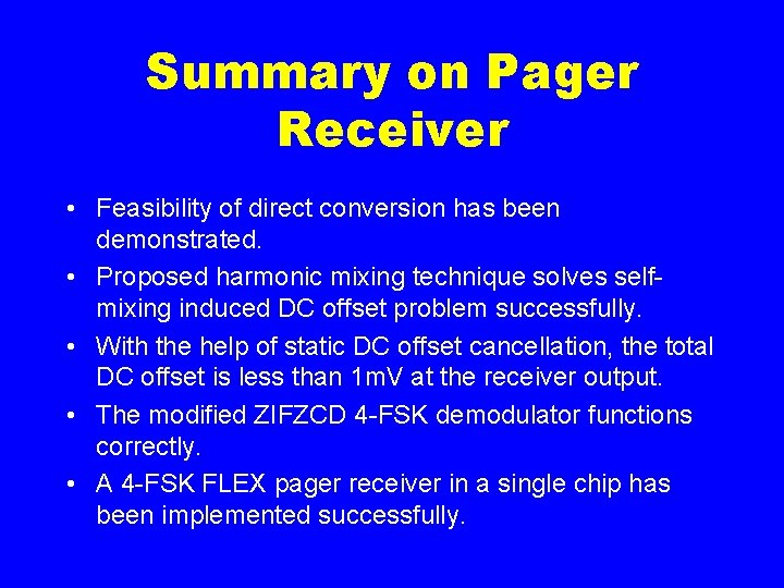
Summary on Pager Receiver • Feasibility of direct conversion has been demonstrated. • Proposed harmonic mixing technique solves selfmixing induced DC offset problem successfully. • With the help of static DC offset cancellation, the total DC offset is less than 1 m. V at the receiver output. • The modified ZIFZCD 4 -FSK demodulator functions correctly. • A 4 -FSK FLEX pager receiver in a single chip has been implemented successfully.

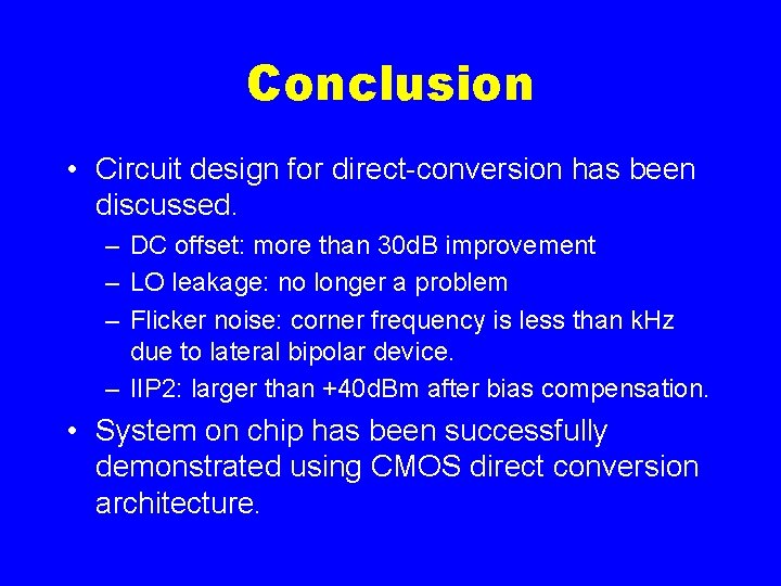
Conclusion • Circuit design for direct-conversion has been discussed. – DC offset: more than 30 d. B improvement – LO leakage: no longer a problem – Flicker noise: corner frequency is less than k. Hz due to lateral bipolar device. – IIP 2: larger than +40 d. Bm after bias compensation. • System on chip has been successfully demonstrated using CMOS direct conversion architecture.