UNITIV Fiber Optical Receivers Photo Detectors Optical receivers
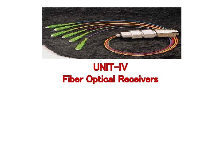
UNIT-IV Fiber Optical Receivers
Photo Detectors • Optical receivers convert optical signal (light) to electrical signal (current/voltage) – Hence referred ‘O/E Converter’ • Photodetector is the fundamental element of optical receiver, followed by amplifiers and signal conditioning circuitry • There are several photodetector types: – Photodiodes, Phototransistors, Photon multipliers, Photo-resistors etc.

Requirements • Compatible physical dimensions (small size) • Wavelength selectivity : Low sensitivity (high responsivity) at the desired wavelength and low responsivity elsewhere • Low noise and high gain • High bandwidth Fast response time • Insensitive to temperature variations • Long operating life and low cost
Photodiodes • Photodiodes meet most of the requirements, hence widely used as photo detectors. • Positive-Intrinsic-Negative (pin) photodiode – No internal gain, robust detector • Avalanche Photo Diode (APD) – Advanced version with internal gain M due to self multiplication process • Photodiodes are sufficiently reverse biased during normal operation no current flow without illumination, the intrinsic region is fully depleted of carriers
PIN Photodiode Ø Semiconductor positive-negative structure with an intrinsic region sandwiched between the other two regions. Ø Normally operated by applying a reverse-bias voltage. Ø Dark current can also be produced which is a leakage current that flows when a reverse bias is applied without incident light.
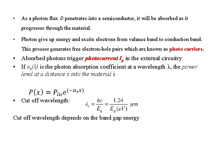
• As a photon flux Φ penetrates into a semiconductor, it will be absorbed as it progresses through the material. • Photon give up energy and excite electrons from valance band to conduction band. This process generates free electron-hole pairs which are known as photo carriers. • Absorbed photons trigger photocurrent Ip in the external circuitry • If αs(λ) is the photon absorption coefficient at a wavelength λ, the power level at a distance x into the material i • Cut off wavelength: Cut off wavelength depends on the band gap energy
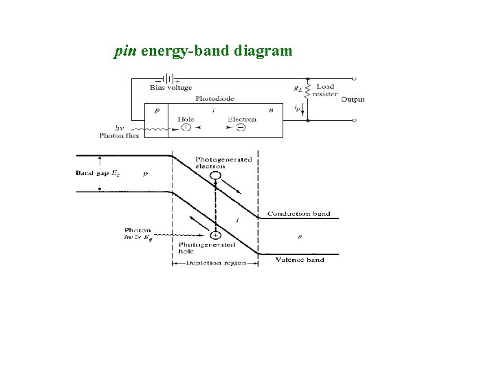
pin energy-band diagram
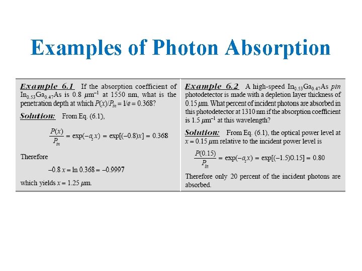
Examples of Photon Absorption
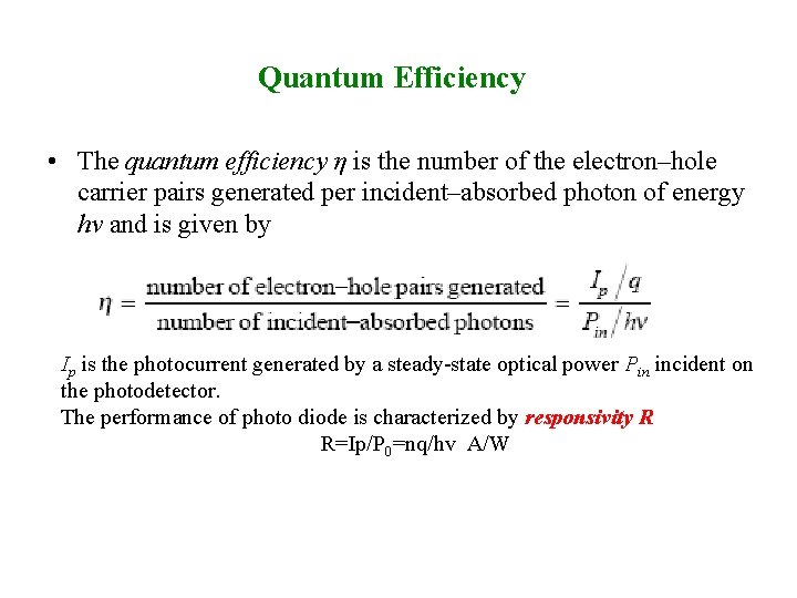
Quantum Efficiency • The quantum efficiency η is the number of the electron–hole carrier pairs generated per incident–absorbed photon of energy hν and is given by Ip is the photocurrent generated by a steady-state optical power Pin incident on the photodetector. The performance of photo diode is characterized by responsivity R R=Ip/P 0=nq/hv A/W
Avalanche Photodiode (APD) • An APD internally amplifies the photocurrent by an avalanche process when a large reverse-bias voltage is applied across the active region. • The gain of the APD can be changed by changing the reversebias voltage. • APD has an internal gain M, which is obtained by having a high electric field that energizes photo-generated electrons. • These electrons ionize bound electrons in the valence band upon colliding with them which is known as impact ionization • The newly generated electrons and holes are also accelerated by the high electric field and gain energy to cause further impact ionization • This phenomena is the avalanche effect

• Diagram
Advantage of PIN photodiodes Ø The output electrical current is linearly proportional to the input optical power making it a highly linear device. Ø Low bias voltage(<4 v). Ø Low noise Ø Low dark current Ø High-speed response
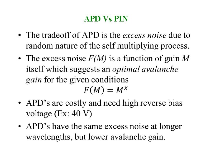
APD Vs PIN •
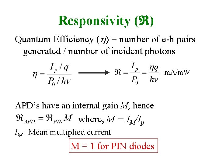
Responsivity ( ) Quantum Efficiency ( ) = number of e-h pairs generated / number of incident photons m. A/m. W APD’s have an internal gain M, hence where, M = IM/Ip IM : Mean multiplied current M = 1 for PIN diodes
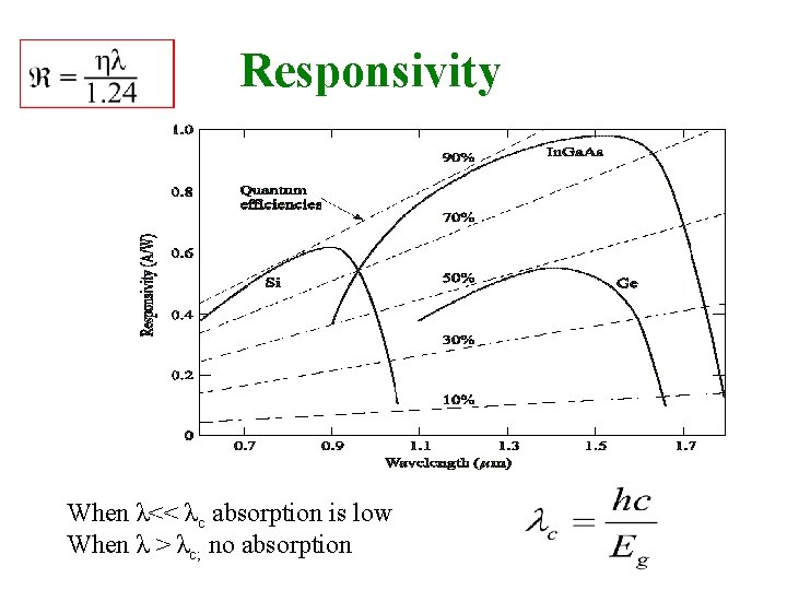
Responsivity When λ<< λc absorption is low When λ > λc; no absorption
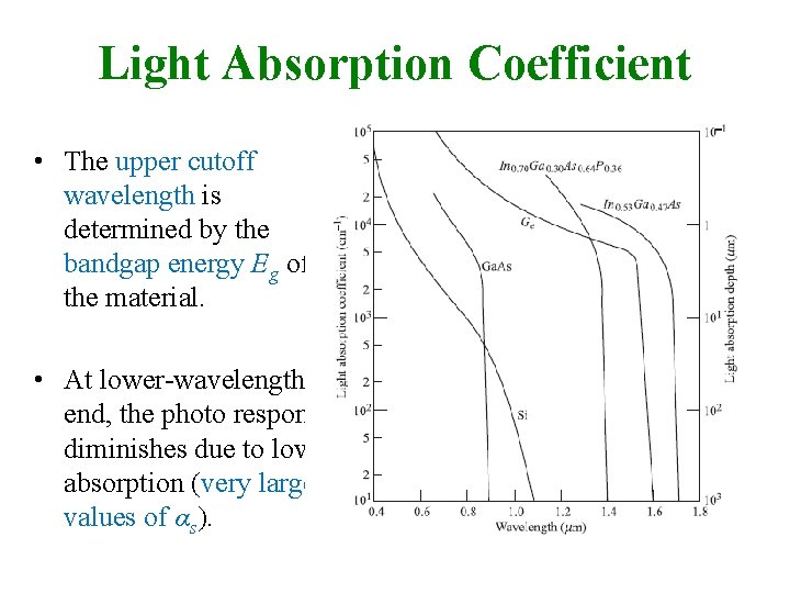
Light Absorption Coefficient • The upper cutoff wavelength is determined by the bandgap energy Eg of the material. • At lower-wavelength end, the photo response diminishes due to low absorption (very large values of αs).
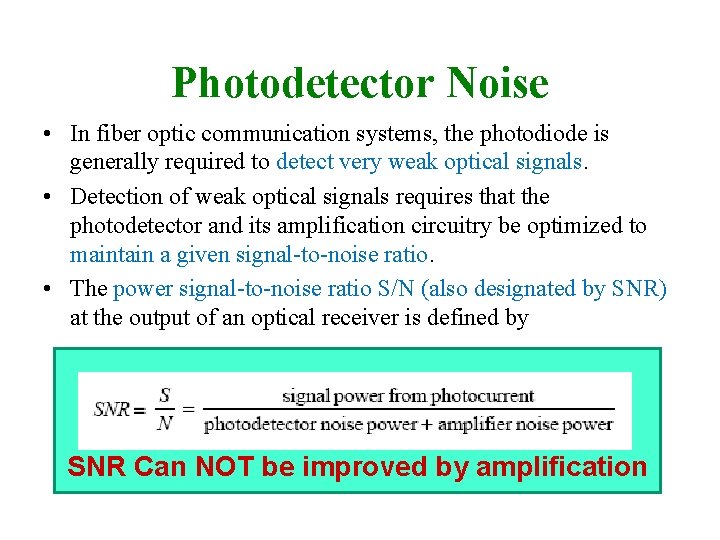
Photodetector Noise • In fiber optic communication systems, the photodiode is generally required to detect very weak optical signals. • Detection of weak optical signals requires that the photodetector and its amplification circuitry be optimized to maintain a given signal-to-noise ratio. • The power signal-to-noise ratio S/N (also designated by SNR) at the output of an optical receiver is defined by SNR Can NOT be improved by amplification
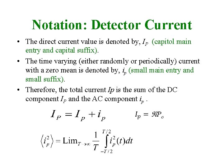
Notation: Detector Current • The direct current value is denoted by, IP (capitol main entry and capital suffix). • The time varying (either randomly or periodically) current with a zero mean is denoted by, ip (small main entry and small suffix). • Therefore, the total current Ip is the sum of the DC component IP and the AC component ip.
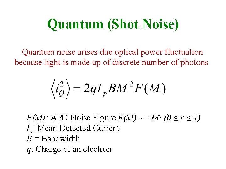
Quantum (Shot Noise) Quantum noise arises due optical power fluctuation because light is made up of discrete number of photons F(M): APD Noise Figure F(M) ~= Mx (0 ≤ x ≤ 1) Ip: Mean Detected Current B = Bandwidth q: Charge of an electron
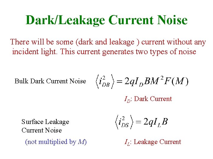
Dark/Leakage Current Noise There will be some (dark and leakage ) current without any incident light. This current generates two types of noise Bulk Dark Current Noise ID: Dark Current Surface Leakage Current Noise (not multiplied by M) IL: Leakage Current
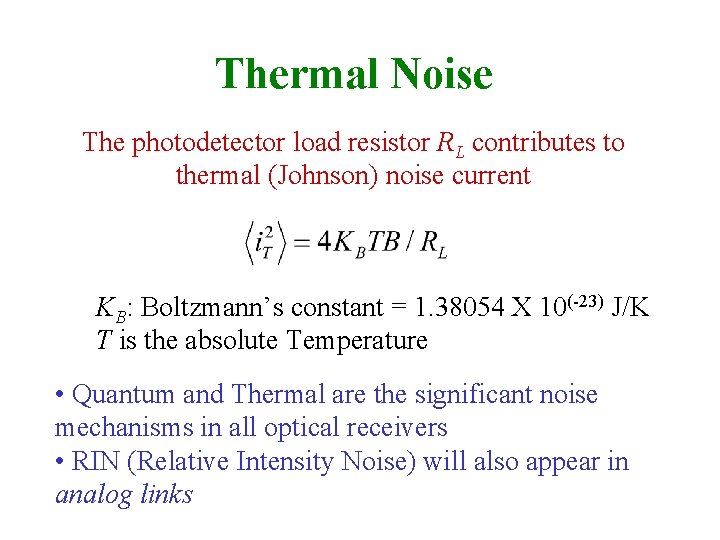
Thermal Noise The photodetector load resistor RL contributes to thermal (Johnson) noise current KB: Boltzmann’s constant = 1. 38054 X 10(-23) J/K T is the absolute Temperature • Quantum and Thermal are the significant noise mechanisms in all optical receivers • RIN (Relative Intensity Noise) will also appear in analog links
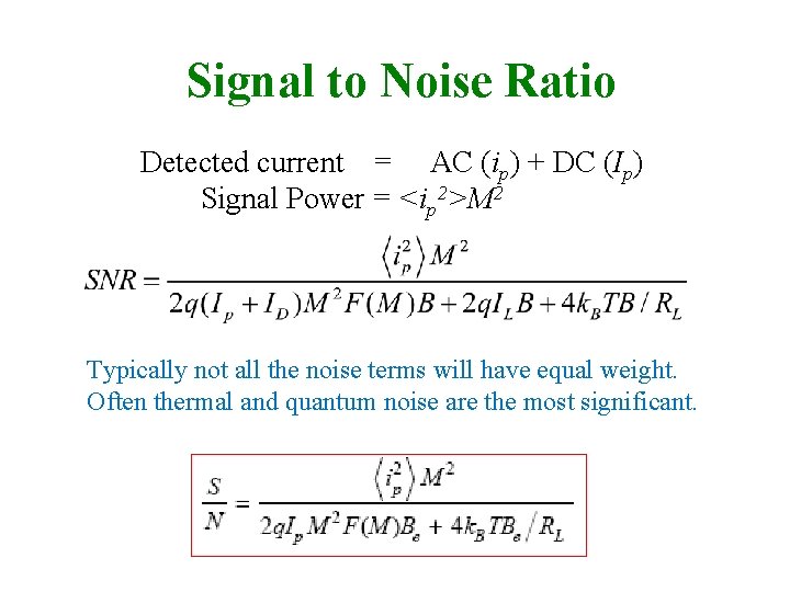
Signal to Noise Ratio Detected current = AC (ip) + DC (Ip) Signal Power = <ip 2>M 2 Typically not all the noise terms will have equal weight. Often thermal and quantum noise are the most significant.
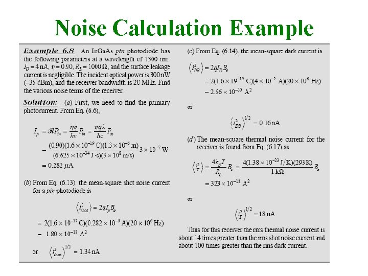
Noise Calculation Example
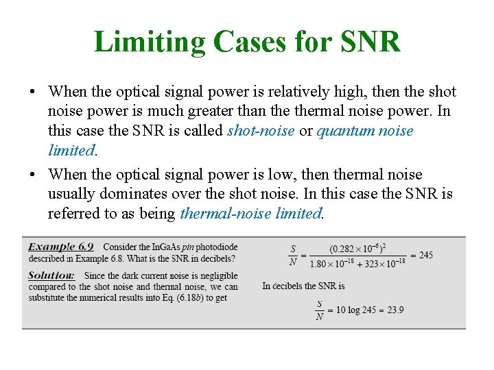
Limiting Cases for SNR • When the optical signal power is relatively high, then the shot noise power is much greater than thermal noise power. In this case the SNR is called shot-noise or quantum noise limited. • When the optical signal power is low, then thermal noise usually dominates over the shot noise. In this case the SNR is referred to as being thermal-noise limited.
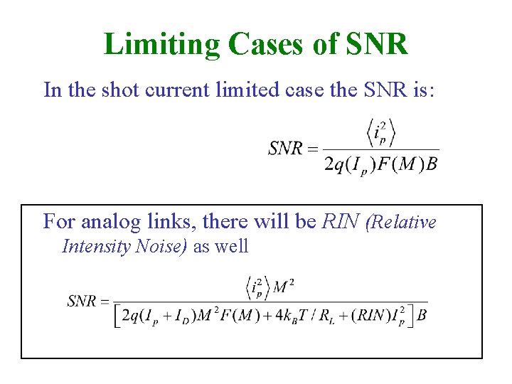
Limiting Cases of SNR In the shot current limited case the SNR is: For analog links, there will be RIN (Relative Intensity Noise) as well
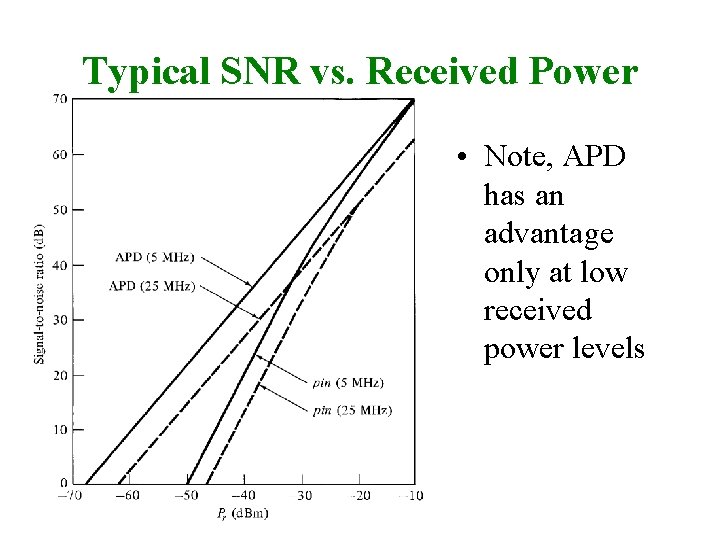
Typical SNR vs. Received Power • Note, APD has an advantage only at low received power levels
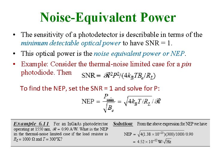
Noise-Equivalent Power • The sensitivity of a photodetector is describable in terms of the minimum detectable optical power to have SNR = 1. • This optical power is the noise equivalent power or NEP. • Example: Consider thermal-noise limited case for a pin photodiode. Then To find the NEP, set the SNR = 1 and solve for P:
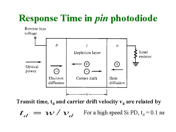
Response Time in photodiode Transit time, td and carrier drift velocity vd are related by For a high speed Si PD, td = 0. 1 ns
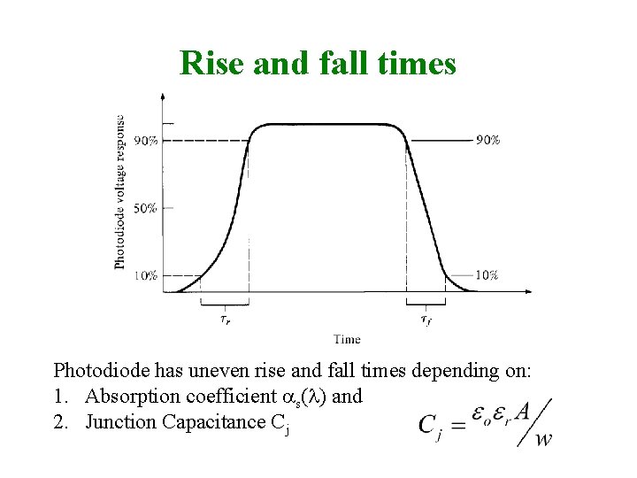
Rise and fall times Photodiode has uneven rise and fall times depending on: 1. Absorption coefficient s( ) and 2. Junction Capacitance Cj
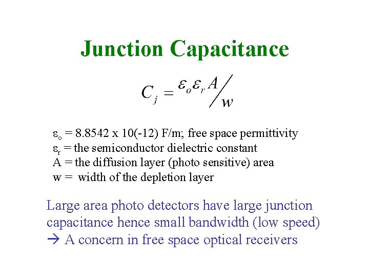
Junction Capacitance εo = 8. 8542 x 10(-12) F/m; free space permittivity εr = the semiconductor dielectric constant A = the diffusion layer (photo sensitive) area w = width of the depletion layer Large area photo detectors have large junction capacitance hence small bandwidth (low speed) A concern in free space optical receivers
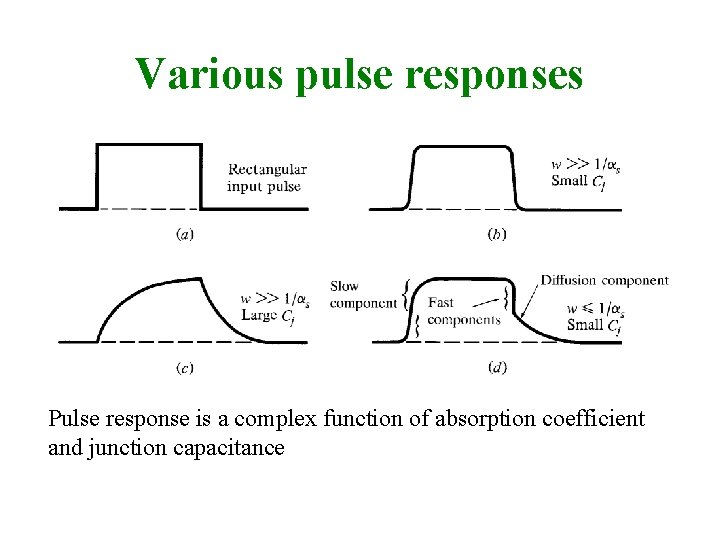
Various pulse responses Pulse response is a complex function of absorption coefficient and junction capacitance
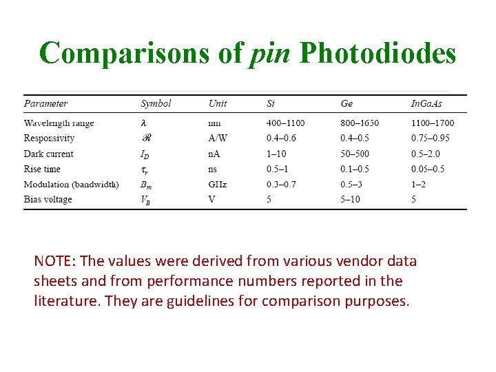
Comparisons of pin Photodiodes NOTE: The values were derived from various vendor data sheets and from performance numbers reported in the literature. They are guidelines for comparison purposes.
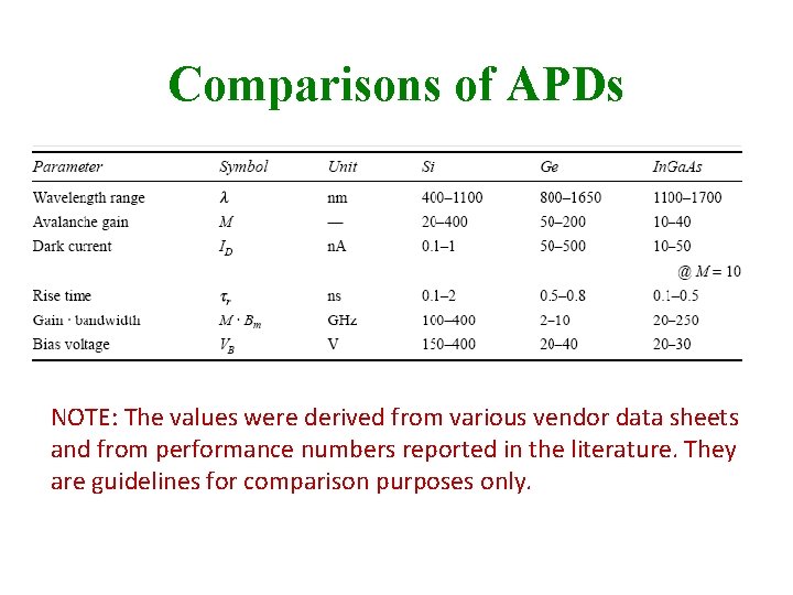
Comparisons of APDs NOTE: The values were derived from various vendor data sheets and from performance numbers reported in the literature. They are guidelines for comparison purposes only.

Fundamental Receiver operation Signal Path through an Optical Link
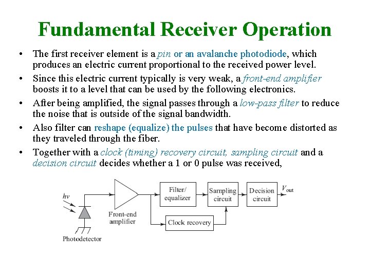
Fundamental Receiver Operation • The first receiver element is a pin or an avalanche photodiode, which produces an electric current proportional to the received power level. • Since this electric current typically is very weak, a front-end amplifier boosts it to a level that can be used by the following electronics. • After being amplified, the signal passes through a low-pass filter to reduce the noise that is outside of the signal bandwidth. • Also filter can reshape (equalize) the pulses that have become distorted as they traveled through the fiber. • Together with a clock (timing) recovery circuit, sampling circuit and a decision circuit decides whether a 1 or 0 pulse was received,
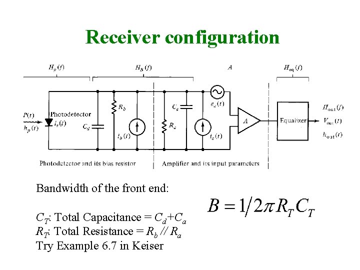
Receiver configuration Bandwidth of the front end: CT: Total Capacitance = Cd+Ca RT: Total Resistance = Rb // Ra Try Example 6. 7 in Keiser
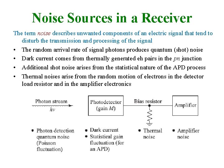
Noise Sources in a Receiver The term noise describes unwanted components of an electric signal that tend to disturb the transmission and processing of the signal • The random arrival rate of signal photons produces quantum (shot) noise • Dark current comes from thermally generated eh pairs in the pn junction • Additional shot noise arises from the statistical nature of the APD process • Thermal noises arise from the random motion of electrons in the detector load resistor and in the amplifier electronics
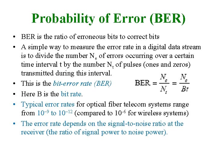
Probability of Error (BER) • BER is the ratio of erroneous bits to correct bits • A simple way to measure the error rate in a digital data stream is to divide the number Ne of errors occurring over a certain time interval t by the number Nt of pulses (ones and zeros) transmitted during this interval. • This is the bit-error rate (BER) • Here B is the bit rate. • Typical error rates for optical fiber telecom systems range from 10– 9 to 10– 12 (compared to 10 -6 for wireless systems) • The error rate depends on the signal-to-noise ratio at the receiver (the ratio of signal power to noise power).
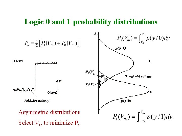
Logic 0 and 1 probability distributions Asymmetric distributions Select Vth to minimize Pe
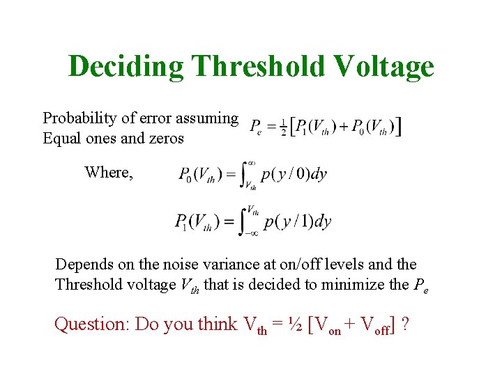
Deciding Threshold Voltage Probability of error assuming Equal ones and zeros Where, Depends on the noise variance at on/off levels and the Threshold voltage Vth that is decided to minimize the Pe Question: Do you think Vth = ½ [Von + Voff] ?
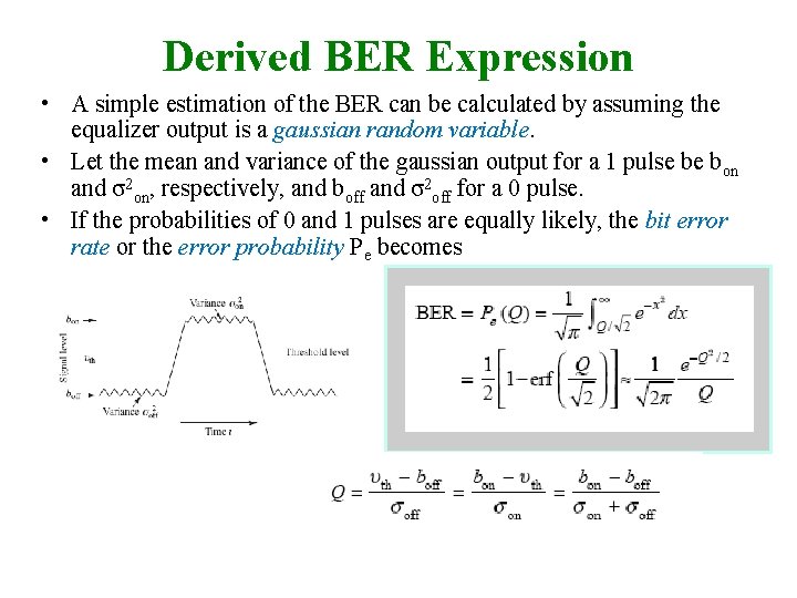
Derived BER Expression • A simple estimation of the BER can be calculated by assuming the equalizer output is a gaussian random variable. • Let the mean and variance of the gaussian output for a 1 pulse be bon and σ2 on, respectively, and boff and σ2 off for a 0 pulse. • If the probabilities of 0 and 1 pulses are equally likely, the bit error rate or the error probability Pe becomes
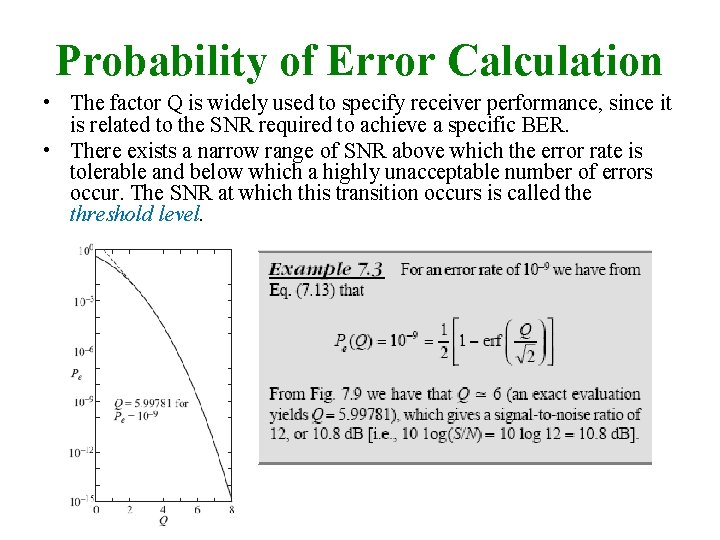
Probability of Error Calculation • The factor Q is widely used to specify receiver performance, since it is related to the SNR required to achieve a specific BER. • There exists a narrow range of SNR above which the error rate is tolerable and below which a highly unacceptable number of errors occur. The SNR at which this transition occurs is called the threshold level.
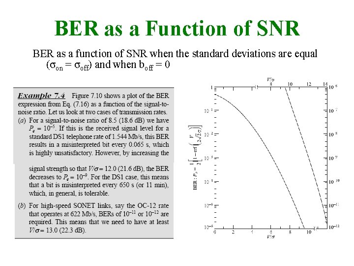
BER as a Function of SNR BER as a function of SNR when the standard deviations are equal (σon = σoff) and when boff = 0
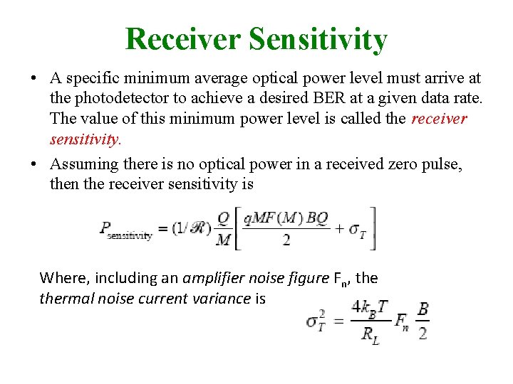
Receiver Sensitivity • A specific minimum average optical power level must arrive at the photodetector to achieve a desired BER at a given data rate. The value of this minimum power level is called the receiver sensitivity. • Assuming there is no optical power in a received zero pulse, then the receiver sensitivity is Where, including an amplifier noise figure Fn, thermal noise current variance is
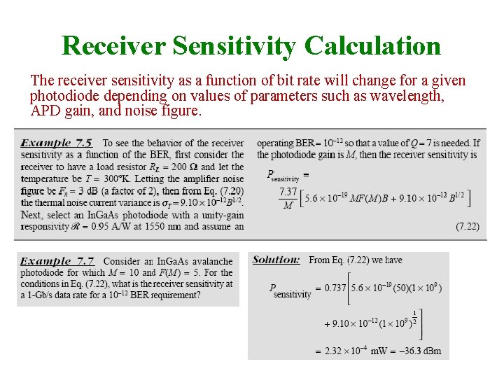
Receiver Sensitivity Calculation The receiver sensitivity as a function of bit rate will change for a given photodiode depending on values of parameters such as wavelength, APD gain, and noise figure.
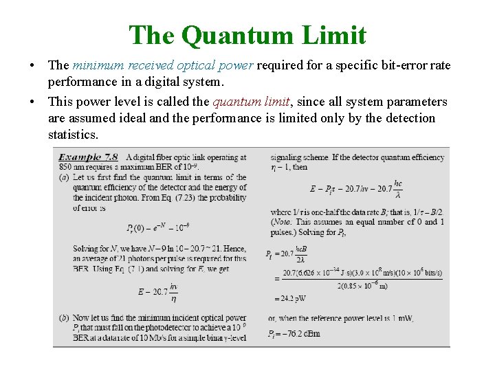
The Quantum Limit • The minimum received optical power required for a specific bit-error rate performance in a digital system. • This power level is called the quantum limit, since all system parameters are assumed ideal and the performance is limited only by the detection statistics.
- Slides: 46