ClassE Power Amplifiers for QRP to QRO David






- Slides: 43

Class-E Power Amplifiers for QRP to QRO David Cripe NMØS Mount Vernon IA August 6, 2011

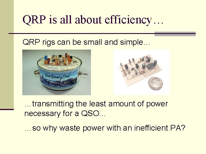
QRP is all about efficiency… QRP rigs can be small and simple… …transmitting the least amount of power necessary for a QSO… …so why waste power with an inefficient PA?

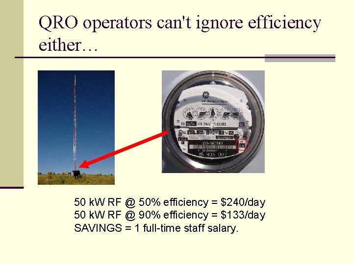
QRO operators can't ignore efficiency either… 50 k. W RF @ 50% efficiency = $240/day 50 k. W RF @ 90% efficiency = $133/day SAVINGS = 1 full-time staff salary.

Why is PA efficiency important? Typical CW ham transmitter has power amplifier efficiency of 50%. A transmitter delivering 5 W RF, at 50% efficiency consumes 10 W battery power. Its PA transistor must be capable of dissipating 5 W power

Why is PA efficiency important? What would happen if PA efficiency of a 5 W transmitter was increased to 90%? Power consumption from battery is reduced from 10 watts to 5. 5 watts Power dissipation in the transistor is reduced to 0. 5 watts, a 90% reduction.

Why is PA efficiency important? A higher efficiency PA will result in: Smaller, cheaper transistor required Cooler operation of PA Higher reliability of PA Reduced battery consumption. Class-E is a simple, rugged, highly-efficient power amplifier circuit capable of operating at 90% efficiency.

What is Class-E? The Class-E Power Amplifier was invented by Nat and Alan Sokal in the 1970 s. It is uses the power device as a switch, and is capable of DC-to-RF efficiency nearing 100%. It uses a low-Q tuned drain network to obtain specially-shaped voltage and current waveforms that minimize transistor losses.

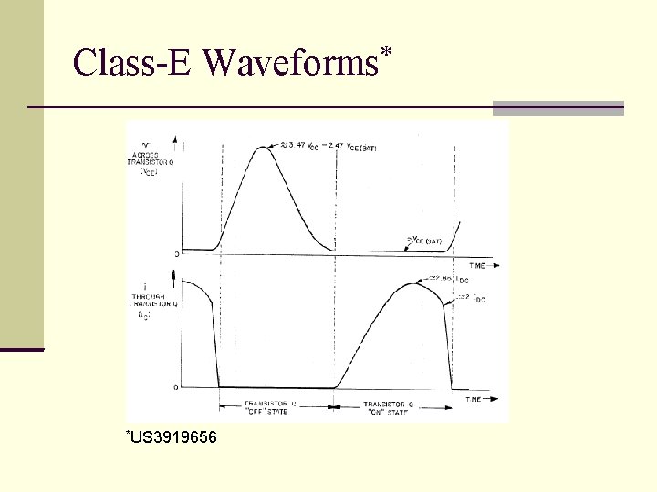
Class-E Waveforms* *US 3919656

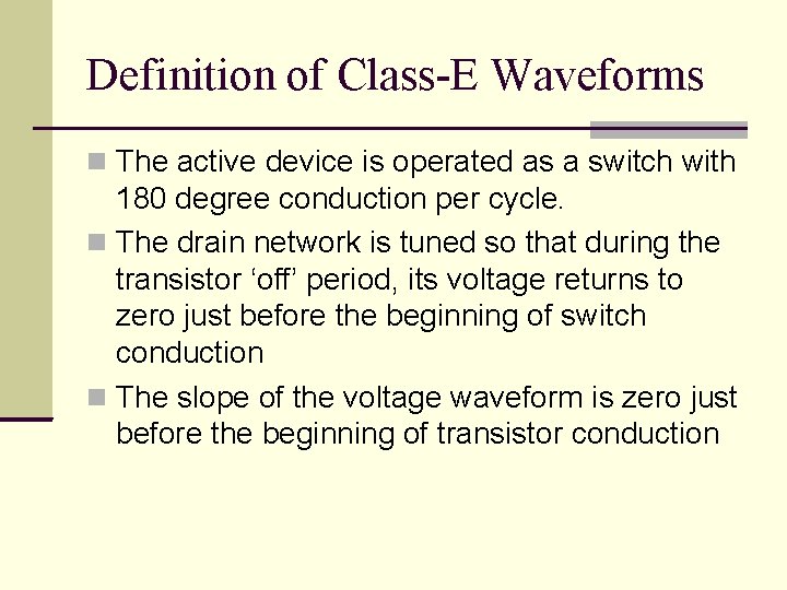
Definition of Class-E Waveforms The active device is operated as a switch with 180 degree conduction per cycle. The drain network is tuned so that during the transistor ‘off’ period, its voltage returns to zero just before the beginning of switch conduction The slope of the voltage waveform is zero just before the beginning of transistor conduction

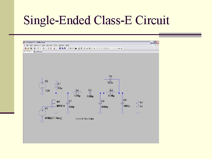
Single-Ended Class-E Circuit

Where can Class-E transmitters be found? Broadcast Electronics SGC Mini-Lini, 4 SQRP NS-40, 1 – 5 KW 500 W ‘linear’ 5 W, 40 M AM BC Transmitter CW Transmitter

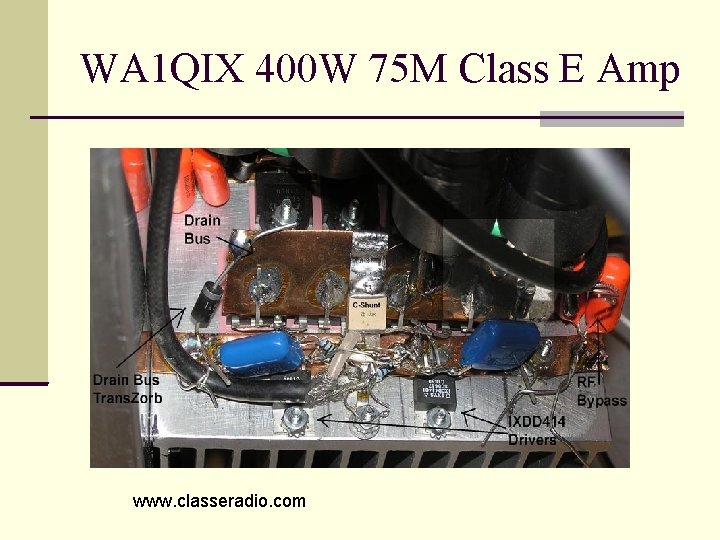
WA 1 QIX 400 W 75 M Class E Amp www. classeradio. com

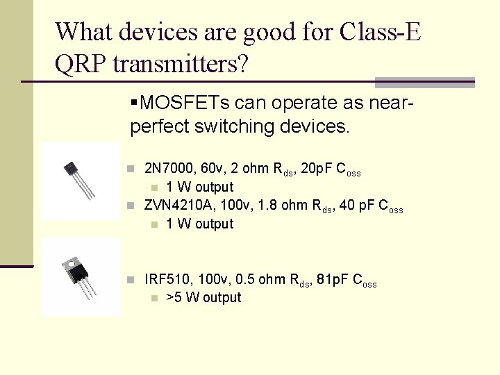
What devices are good for Class-E QRP transmitters? MOSFETs can operate as nearperfect switching devices. 2 N 7000, 60 v, 2 ohm Rds, 20 p. F Coss 1 W output ZVN 4210 A, 100 v, 1. 8 ohm Rds, 40 p. F Coss 1 W output IRF 510, 100 v, 0. 5 ohm Rds, 81 p. F Coss >5 W output

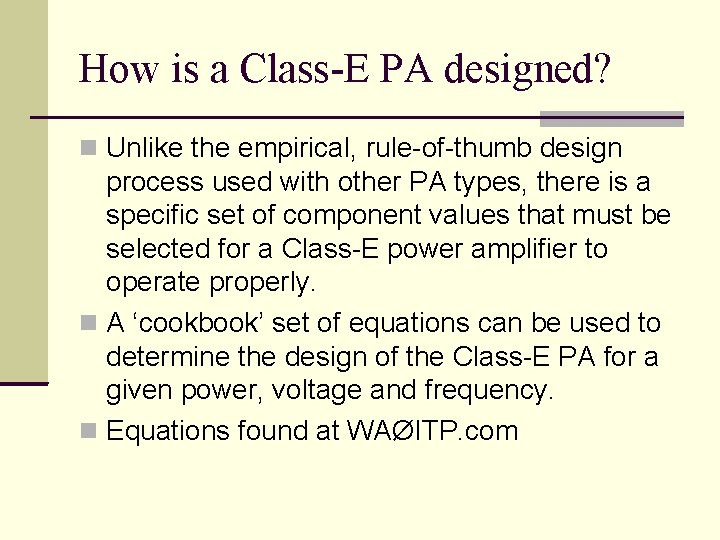
How is a Class-E PA designed? Unlike the empirical, rule-of-thumb design process used with other PA types, there is a specific set of component values that must be selected for a Class-E power amplifier to operate properly. A ‘cookbook’ set of equations can be used to determine the design of the Class-E PA for a given power, voltage and frequency. Equations found at WAØITP. com

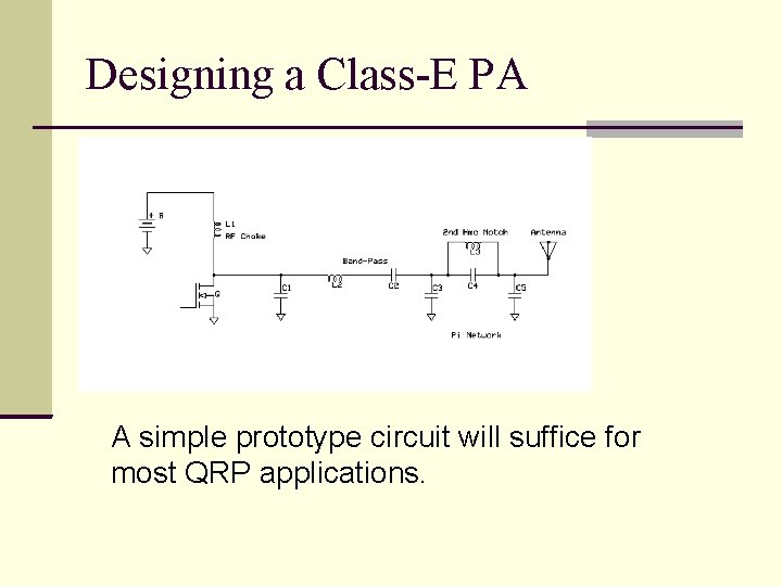
Designing a Class-E PA A simple prototype circuit will suffice for most QRP applications.

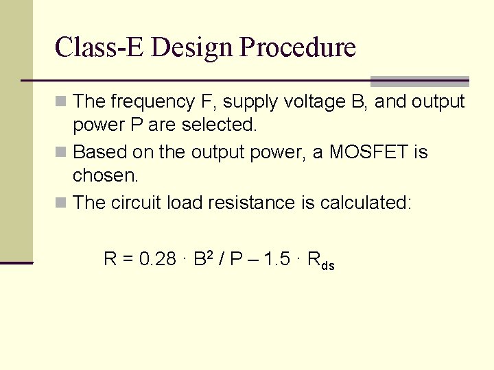
Class-E Design Procedure The frequency F, supply voltage B, and output power P are selected. Based on the output power, a MOSFET is chosen. The circuit load resistance is calculated: R = 0. 28 · B 2 / P – 1. 5 · Rds

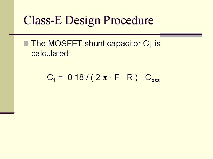
Class-E Design Procedure The MOSFET shunt capacitor C 1 is calculated: C 1 = 0. 18 / ( 2 · F · R ) - Coss

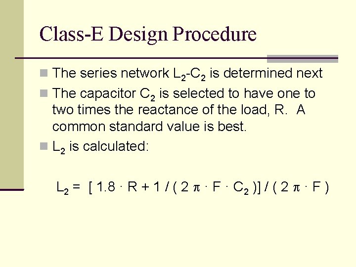
Class-E Design Procedure The series network L 2 -C 2 is determined next The capacitor C 2 is selected to have one to two times the reactance of the load, R. A common standard value is best. L 2 is calculated: L 2 = [ 1. 8 · R + 1 / ( 2 · F · C 2 )] / ( 2 · F )

Class-E Design Procedure The load impedance of the PA must be transformed to 50 ohms. A preferred way to achieve this is with a 90 degree PI network. A second-harmonic notch is added to the series inductor L 3.

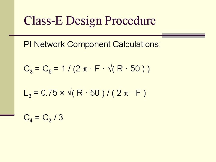
Class-E Design Procedure PI Network Component Calculations: C 3 = C 5 = 1 / (2 · F · √( R · 50 ) ) L 3 = 0. 75 × √( R · 50 ) / ( 2 · F ) C 4 = C 3 / 3

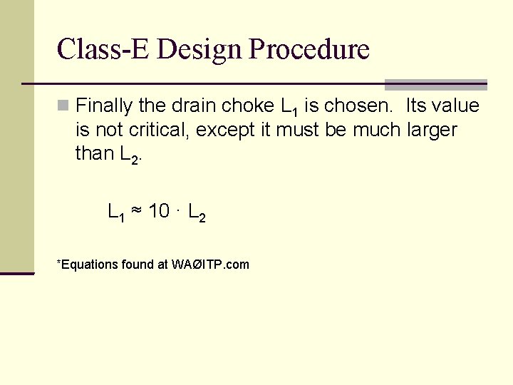
Class-E Design Procedure Finally the drain choke L 1 is chosen. Its value is not critical, except it must be much larger than L 2. L 1 ≈ 10 · L 2 *Equations found at WAØITP. com

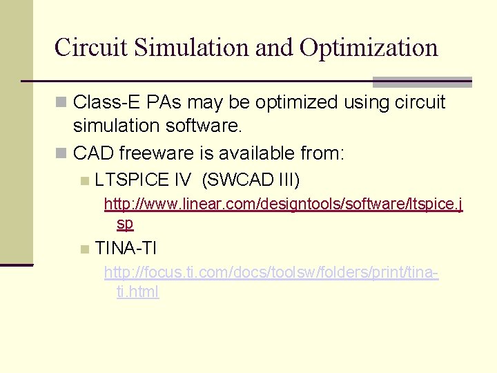
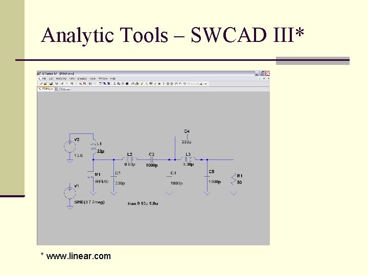
Circuit Simulation and Optimization Class-E PAs may be optimized using circuit simulation software. CAD freeware is available from: LTSPICE IV (SWCAD III) http: //www. linear. com/designtools/software/ltspice. j sp TINA-TI http: //focus. ti. com/docs/toolsw/folders/print/tinati. html

Analytic Tools – SWCAD III* * www. linear. com

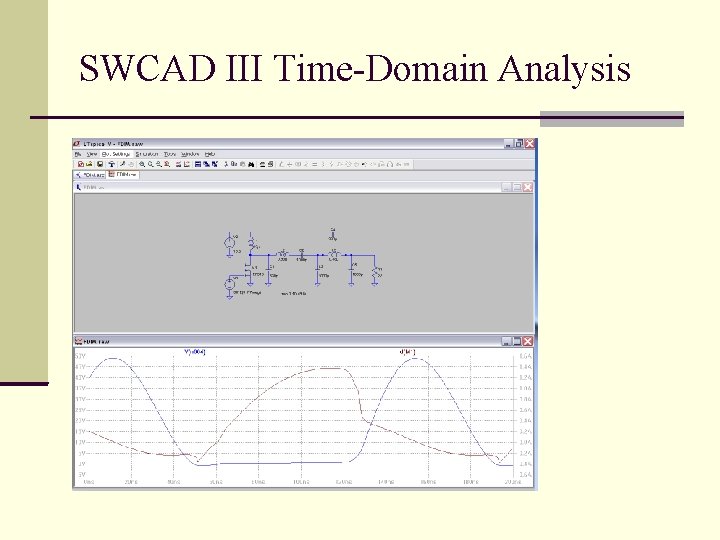
SWCAD III Time-Domain Analysis

Efficiency and Thermal Management The heat loss in the MOSFET will be approximately 2 P Rds / R. A good rule of thumb for MOSFET reliability is to keep the junction temperature below 100 degrees C. We can estimate MOSFET junction temperature from thermal resistance data in manufacturers’ data sheets.

Thermal Impedance A TO-92 transistor (2 N 7000) has 312 degrees C-per-watt thermal resistance. Allowable dissipation in a TO-92 part is about ¼ watt. A TO-220 transistor (IRF 510) has 62 degrees C-per-watt thermal resistance. Allowable dissipation in a TO-220 is >1 W Adding a heat sink to a TO-220 can further increase allowable dissipation.

How is the Class-E PA driven? A MOSFET is a voltage-controlled device. The gate of a MOSFET is a relatively large capacitance. The MOSFET driver circuit must handle the large currents required to charge and discharge the gate capacitance at the carrier frequency.

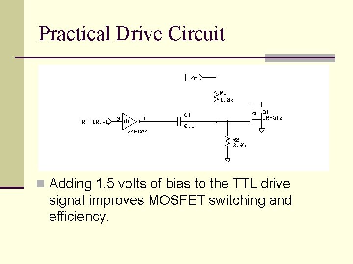
Practical MOSFET Drive Circuitry Many MOSFETs are designed to be driven directly from TTL-level signals. TTL Drive requires NO transformer or impedance matching. One 74 HCxx gate can drive a 2 N 7000 up to 14 MHz, two, paralleled 74 HCxx gates can drive an IRF 510 up to 7 MHz. 74 ACxx logic has 4 x drive capability of 74 HCxx.

Practical Drive Circuit Adding 1. 5 volts of bias to the TTL drive signal improves MOSFET switching and efficiency.

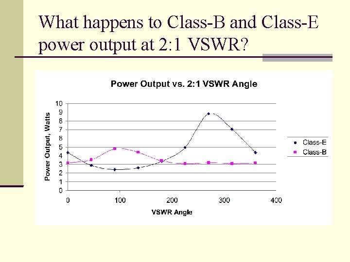
How do the Class-B and –E PAs compare? SWCAD III simulations of IRF 510, 5 W Class- E and Class-B PAs were compared in normal operation into a 1: 1 VSWR. The Class-B PA operated at 71% efficiency, while the Class-E PA operated at 92% efficiency. The performance of the Class-B and –E circuits were then compared over eight points on a 2: 1 VSWR circle.

What happens to Class-B and Class-E power output at 2: 1 VSWR?

Transistor Dissipation vs. VSWR

Efficiency vs. VSWR

Peak Drain V vs. VSWR, Class-E

Class-E Harmonic Performance Harmonic content at drain of MOSFET A second harmonic notch is usually required to provide sufficient attenuation!

Class-E LINEAR Amplifier ARRL Homebrew Challenge 50 W 40 M linear amplifier LOWEST cost design goal!

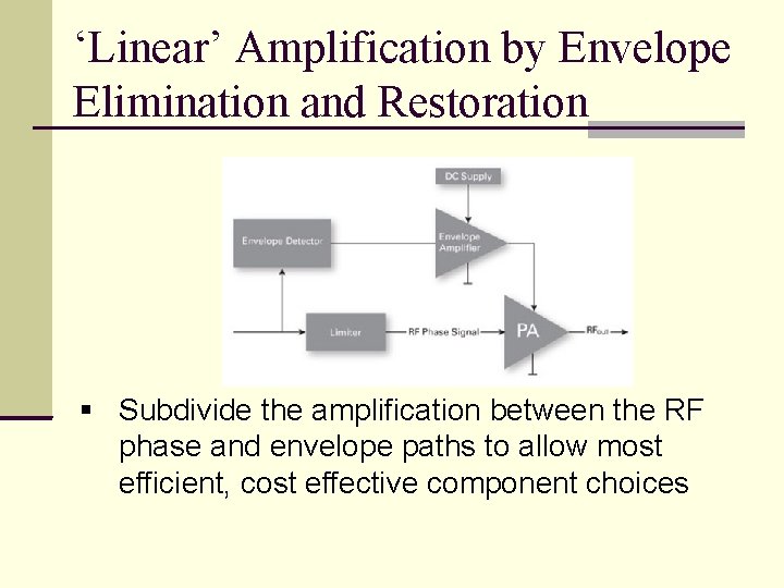
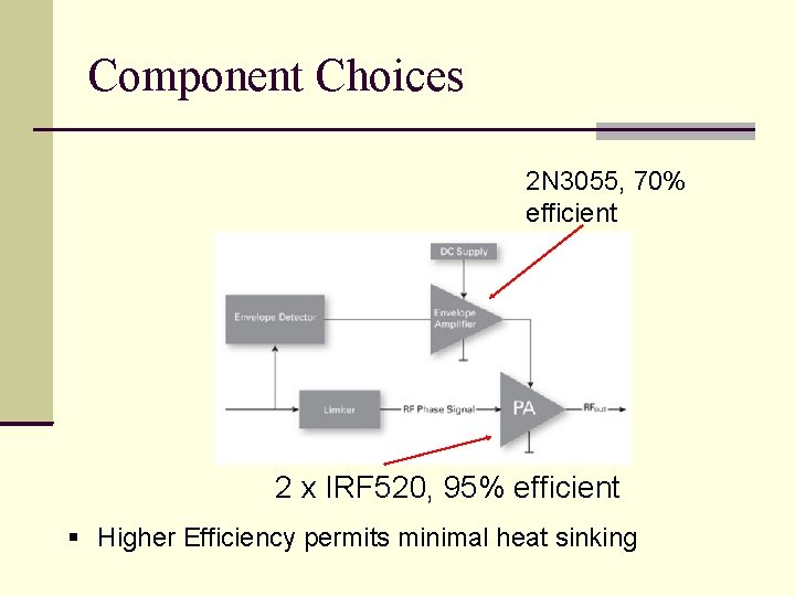
Strategies for Low Cost Design: Highest components in PA are RF power devices, heat sinks, enclosure. Solution: Envelope-Elimination-and. Restoration Architecture Uses cheap, efficient MOSFETs in Class-E CW amplifier, cheap, slow BJT in linear envelope amplifier. Minimal heat sink required.

‘Linear’ Amplification by Envelope Elimination and Restoration Subdivide the amplification between the RF phase and envelope paths to allow most efficient, cost effective component choices

Component Choices 2 N 3055, 70% efficient 2 x IRF 520, 95% efficient Higher Efficiency permits minimal heat sinking

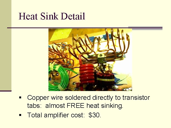
Heat Sink Detail Copper wire soldered directly to transistor tabs: almost FREE heat sinking. Total amplifier cost: $30.

Conclusions Class-E Power Amplifiers offer a significant improvement in transmitter efficiency over other designs. This results in reduced heating of the PA transistor, reduced battery consumption. The circuits are simple to design and construct using a cookbook approach. They are an extremely good choice for singleband CW transmitters.

But… Class-E circuits do not easily lend themselves to multi-band operation. Their output power is controlled by supply voltage (not a linear amplifier). The low-Q output network requires attention to the 2 nd harmonic. Watch the VSWR, especially when using 60 volt MOSFETs!

Class-E Power Amplifiers for QRP Questions?