Chapter 3 Special Purpose Diodes ZENER DIODE ELECTRONIC


 is increased – the reverse current (IR)")


 When current is 25 m. A For Iz=25 m. A: The 25 m.")


")


:")
:")


, let analyze the circuit…zener diode connected")
: � So,")
 Determine VOUT at IZK and IZM (b)")
 Determine")
 Determine minimum and maximum load current for which the zener diode can maintain")

 Determine the minimum value of RL that can be used")
 Determine the minimum and maximum load current for")


- Slides: 55
Chapter 3 Special Purpose Diodes -ZENER DIODE- ELECTRONIC DEVICES EET 109 PERANTI ELEKTRONIK
OBJECTIVE Ø Describe the characteristic of zener diode and analyze its operation. Ø Explain how a zener diode is used in voltage reference, regulation and limiting applications. Ø Troubleshoot zener diode regulators.
CONTENT � � Zener diode applications Troubleshooting Summary
INTRODUCTION Ø Ø Ø Zener diode – silicon pn-junction device that is designed for operation in the reverse-breakdown region. The basic function of zener diode is to maintain a nearly constant dc voltage under properating condition. Typically it is used to provide a stable reference voltage for use in power supplies, voltmeter and other equipment. Zener diode symbol
INTRODUCTION Ø Breakdown voltage – set by controlling the doping level during manufacture. Ø When diode reached reverse breakdown – voltage remains constant even though current change drastically. Ø If zener diode is FB – operates the same as a rectifier diode. Ø A zener diode is much like a normal diode – but it is placed in the circuit in reverse bias and operates in reverse breakdown. Ø Note that it’s forward characteristics are just like a normal diode.
INTRODUCTION General diode V-I characteristic
ZENER BREAKDOWN Ø Two types of reverse breakdown: avalanche breakdown & zener breakdown Ø i) avalanche breakdown - occurs in both rectifier & zener diodes at high reverse voltage - breakdown voltage greater than approximately 5 V Ø ii) zener breakdown - occurs at relatively low reverse voltage - a zener diode is heavily doped to reduce breakdown voltage - this causes very thin depletion region - as a result, intense electric field exists within the depletion region - Near zener breakdown voltage (Vz), the field have enough energy to pull electrons from their valence bands and create current. Ø Note: both type called zener diode (breakdown voltages of 1. 8 V – 200 V)
CHARACTERISTIC CURVE
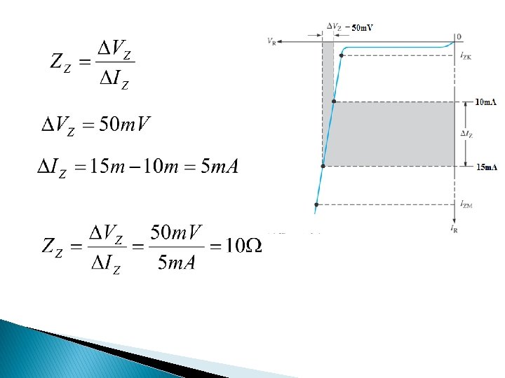
BREAKDOWN CHARACTERISTIC � The reverse voltage (VR) is increased – the reverse current (IR) remains extremely small up to the “knee” of the curve. � Reverse current – called the zener current, IZ. � At that point, breakdown effect begin where zener impedance (Zz) begin to decrease as IZ increases rapidly. � At the bottom of the knee- the zener breakdown voltage (VZ) remains constant although it increase slightly as the zener current, IZ increase. � IZK – min. current required to maintain voltage regulation � IZM – max. amount of current the diode can handle without being damage/destroyed � IZT – the current level at which the VZ rating of diode is measured (specified on a data sheet) � The zener diode maintains nearly constant voltage for value of reverse current rating from IZK to IZM
ZENER EQUIVALENT CIRCUIT Zener impedance Zener diode equivalent circuit model and the Characteristic curve illustrating Zz
ZENER EQUIVALENT CIRCUIT � Since the actual voltage is not ideally vertical, the change in zener current produces a small change in zener voltage � By ohm’s law: � Normally -Zz is specified at IZT. � In most cases, assume Zz is constant over full range of zener current values and is purely resistive.
Example A Zener diode exhibits a certain change in Vz for a certain change in Iz on a portion of the linear characteristic curve between IZK and IZM as illustrated in Figure below. What is Zener impedance?
Exercise � Calculate the Zener Impedance Ans: 2Ω
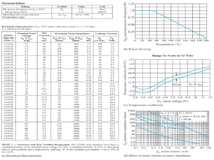
TEMPERATURE COEFFICIENT & ZENER POWER DISSIPATION & DERATING � As with most devices, zener diodes have given characteristics such as temperature coefficients and power ratings that have to be considered. � The data sheet provides this information (refer Figure 3 -7).
Absolute Maximum Ratings � The maximum power dissipation, PD is specified as 1. 0 W up tp 50°C. � The power dissipation is derated (on datasheet) at 6. 67 m. V for each degree above 50°C. � Maximum reverse current, IZM is not specified on datasheet but can be determined from maximum power dissipation for a given value of VZ.
Example From the datasheet, a 1 N 4736 A zener diode has ZZ of 3. 5Ω. The datasheet gives Vz=6. 8 V at a test current Iz of 37 m. A. What is the voltage across zener terminals when: (a) The current is 50 m. A (b) The current is 25 m. A
When the current is 50 m. A For Iz=50 m. A: The 50 m. A current is 13 m. A increase above the test current, Iz of 37 m. A (a) The change in voltage due to the increase in current above the Iz value causes the zener terminal voltage to increase
(b) When current is 25 m. A For Iz=25 m. A: The 25 m. A current is 12 m. A decrease below the test current, Iz of 37 m. A The change in voltage due to the decrease in current below the IZT value causes the zener terminal voltage to decrease.
Exercise Calculate the voltage across zener terminal for a 1 N 4742 A zener diode when: (a) The current is 10 m. A (b) The current is 30 m. A Ans: (a) Vz=11. 901 V (b) Vz=12. 081 V
ZENER DIODE APPLICATIONS � Zener diode can be used as: ØVoltage regulator to provide stable reference voltage. ØSimple limiter or clipper
ZENER REGULATION WITH A VARYING INPUT VOLTAGE � As i/p voltage varies (within limits) – zener diode maintains a constant o/p voltage � As VIN changes, IZ will change proportionally, so i/p voltage variations are set by the min. & max. current value (IZK & IZM) with which the zener can operate. � Resistor, R –current limiting resistor
Example 1: 1 N 4740 10 V zener diode, Find the Min and Max Input Voltage that can regulate the zener diode to maintain an approximate 10 V, Note: Zener impedance neglected (Ideal Model) i/p vary from 10. 055 V – 32 V Maintain o/p voltage
Minimum current Izk Maximum current Izm
Based on Data Sheet
ZENER REGULATION WITH A VARYING INPUT VOLTAGE � From data sheet, 1 N 4740 10 V zener diode maintain regulation from IZK=0. 25 m. A to IZM=100 m. A. � So, � For min. zener current, the voltage across the 220 ohm resistor: � Since VR = VIN - VZ, � For max. zener current, the voltage across resistor is: � Thus
Example Determine the minimum and maximum input voltage that can be regulated by the zener diode in Figure below
From the datasheet VZ=5. 1 V, IZ=49 m. A ZZ=7Ω IZK=1 m. A Assume ZZ over the range of current values. The equivalent circuit: -Vin+VR+Vout=0 Vin = VR+Vout
The maximum zener current, IZM For minimum Input voltage, Vin(min):
For maximum Input voltage, Vin(max):
exercise Determine the minimum and maximum input voltage that can be regulated if 1 N 4736 A zener diode is used in Figure below Ans: Vin(min)=6. 774 V Vin(max)=21. 8911 V
ZENER REGULATION WITH A VARIABLE LOAD � In this illustration of zener regulation circuit, the zener diode will “adjust” its impedance based on varying input voltages and loads (RL) to be able to maintain its designated zener voltage. � Zener current will increase or decrease directly with voltage input changes. The zener current will increase or decrease inversely with varying loads. Again, the zener has a finite range of operation. Note: The zener diode maintains a nearly constant voltage across RL as long as the zener current is greater than IZK and less than IZM
FROM NO LOAD TO FULL LOAD � When output terminal of zener diode is open (RL= ), the load current is zero. � All of the current is through the zener =>no-load condition. � When RL is connected, current is flow through zener and RL. � The total current through R is constant as long as zener is regulating. � As RL decreases, load current IL increases, IZ decreases. � Zener diode continues to regulate the voltage until IZ reaches its minimum value, IZK. � At this point, IL is maximum and full-load condition exists.
Example 2 � Determine the minimum and maximum load current for which the zener diode will maintain regulation. What is the minimum RL that can be used? VZ=12 V, IZK=1 m. A and IZM=50 m. A. Assume ZZ=0Ω and VZ remains a constant 12 V over range of current values.
Solution question 2 � Step 1: When IL=0 A (RL= the total current, IT. ), IZ is maximum and equal to � Step 2: IZ(max) is less than IZM, so 0 A is min. value for IL because zener can handle all of 25. 5 m. A. RL can be removed from the circuit. IL(min) = 0 A � Step 3: The max value of IL occurs when IZ is min (IZ=IZK) � Step 4: The minimum value of RL is:
Example 3 � Figure below shows a 1 N 4733 zener regulated circuit. Given VZ = 10 V at IZT = 10 m. A, IZK = 5 m. A, ZZ = 20 and IZM = 20 m. A. Determine the maximum permissible load currents.
First step. . � The change in zener voltage, � The change in zener current, � Zener voltage for min and max values are: � Maximum and minimum zener current: � Maximum and minimum load current:
From example 3. . � To find IL(max), let analyze the circuit…zener diode connected in parallel with load resistor, RL. For parallel circuit, V same but I is different. � A certain amount of I from source will flow through zener diode and RL. If I through zener diode is max, I flow through RL is min. If I through zener diode is min, I through RL is max. V for both zener and RL is the SAME. � So, when current through zener diode, IZ is min, VZ also min. On the other hand, IL will be max as well as VL max. � Now, find VZ(min) from the formula.
Solution. . � The change in zener current is: � Find VZ(min): � So, VZ(min)=9. 9 V. Then, we need to find total current through the circuit, IZ(min). Using the formula, � Finally find IL(max) using the formula below. Given in the question, IZK=5 m. A. So, IL(max) is
Example 4 For the circuit below: (a) Determine VOUT at IZK and IZM (b) Determine minimum and maximum load current for which the zener diode can maintain regulation (c) Determine the minimum value of RL that can be used
From datasheet, Vz=15 V IZ=17 m. A ZZ=14Ω IZK=0. 25 m. A (a) Determine VOUT at IZK and IZM For IZK: For IZM:
(b) Determine minimum and maximum load current for which the zener diode can maintain regulation For ILmin: When IL=0 (RL=∞), IZ is maximum and equal to IT; Since Izmax is less than IZM, 0 A is an acceptable minimum value for IL because the zener can handle all of the 47. 7487 m. A. If Izmax is greater than IZM, ILmin=Izmax-IZM
For ILmax:
(c) Determine the minimum value of RL that can be used
exercise For the circuit below: (a) Determine the minimum and maximum load current for which the zener diode can maintain regulation (b) What is the minimum value of RL that can be used? Ans: IL(min) =68. 125 m. A IL(max) =127 m. A RLmin=155. 36Ω
ZENER LIMITING Ø Zener diode also can be used in ac applications to limit voltage swings to desired level a) To limit the +ve peak of a signal voltage to the selected zener voltage � During –ve alternation, zener acts as FB diode & limits the –ve voltage to -0. 7 V b) Zener diode is turn around � The –ve peak is by FB zener action & +ve voltage is limited to +0. 7 V c) Two back-to-back zeners limit both peaks to the zener voltage ± 0. 7 V � During the +ve alternation, D 2 is functioning as the zener limiter – D 1 is functioning as a FB diode. � During the –ve alternation-the roles are reversed
Basic zener limiting action with a sinusoidal input voltage
Example 4 � Determine the output voltage for each limiting circuit shown below.
Solution example 4 � When one zener is operating in breakdown, the other one is FB with approximately 0. 7 V across it. For figure a, during +ve cycle, D 1(3. 3 V) FB while D 2(5. 1 V) is zener limiter. For figure b, D 1(6. 2 V) is zener limiter and D 2(15 V) is FB during +ve cycle.
OTHER TYPES OF DIODE v v v v Optical Diode Current Regulator Diode Schottky Diode PIN Diode Step-recovery Diode Tunnel Diode Laser Diode
TROUBLESHOOT � Although precise power supplies typically use IC type regulators, zener diodes can be used alone as a voltage regulator. As with all troubleshooting techniques we must know what is normal. A properly functioning zener will work to maintain the output voltage within certain limits despite changes in load.
TROUBLESHOOT � With an open zener diode, the full unregulated voltage will be present at the output without a load. In some cases with full or partial loading an open zener could remain undetected. no voltage dropped between the filtered o/p of the power supply & the o/p terminal undetected
TROUBLESHOOT � With excessive zener impedance the voltage would be higher than normal but less than the full unregulated output. The zener has failed such that its internal impedance is more than it should be.
SUMMARY Ø The zener diode operates in reverse breakdown. Ø A zener diode maintains a nearly constant voltage across its terminals over a specified range currents. is the maintenance of a Ø Lineofregulation specific voltage with changing input voltages. Ø Load regulation is the maintenance of a specific voltage for different loads.