VARACTOR DIODE A Varicap Diode Varactor Diode Variable

VARACTOR DIODE • A Varicap • • Diode, Varactor Diode, Variable Capacitance Diode, Variable Reactance Diode or Tuning Diode Varactor diode is a p-n junction diode whose capacitance is varied by varying the reverse voltage. Varactors are operated in a reverse-biased state. No current flows, but since thickness of the depletion zone varies with the applied bias voltage, the capacitance of the diode can be made to vary. A varactor diode is best explained as a variable capacitor. Think of the depletion region as a variable dielectric.

VARACTOR DIODE

• They are also called voltage-variable capacitance diodes. • A Junction diode which acts as a variable capacitor under changing reverse bias is known as VARACTOR DIODE. • Capacitance for varactor dide are Pico farad. (10 -12 ) range. Applications • used for high frequencies and switching applications. • used for electronic tuning applications in FM radio s and televisions. • used as voltage-controlled capacitors(voltage-controlled oscillators, parametric amplifiers, and frequency multipliers)
 • A tunnel diode or Esaki diode is a")
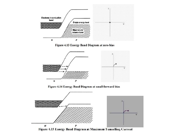
TUNNEL DIODE (ESA KI DIODE) • A tunnel diode or Esaki diode is a type of semiconductor that is capable of very fast operation, well into the microwave frequency region, made possible by the use of the quantum mechanical effect called tunneling. • Heavily-doped p-n junction. Impurity concentration is 1 part in 10^3. • Width of the depletion layer is very small (about 10 0 A). It is generally made up of Ge and Ga. As.

Forward bias operation Under normal forward bias operation, as voltage begins to increase, electrons at first tunnel through the very narrow p–n junction barrier because filled electron states in the conduction band on the n-side become aligned with empty valence band hole states on the p-side of the p-n junction. As voltage increases further these states become more misaligned and the current drops – this is called negative resistance Reverse bias operation When used in the reverse direction, tunnel diodes are called back diodes and can act as fast rectifiers with zero offset voltage and extreme linearity for power signals. Under reverse bias, filled states on the p-side become increasingly aligned with empty states on the n-side and electrons now tunnel through the pn junction barrier in reverse direction
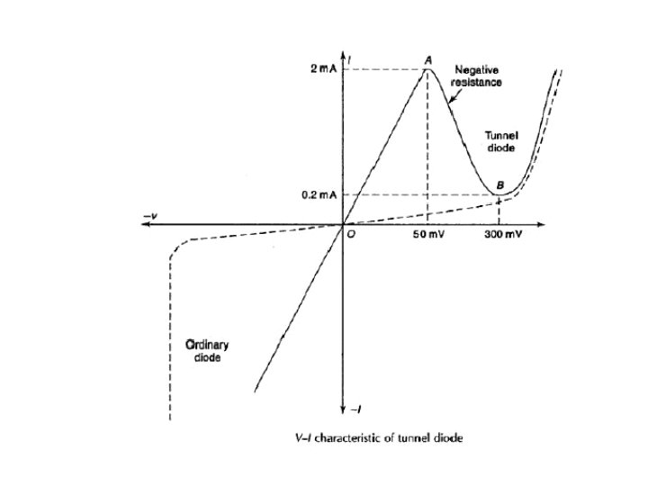

Applications · As logic memory storage device · As microwave oscillator · In relaxation oscillator circuit · As an amplifier ·As an ultra-high speed switch Advantages · Very high speed · Longevity: Disadvantages · Reproducibility: . · Low peak to valley current ratio:
 is a compound of the elements")
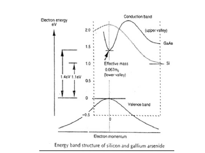
GALLIUM ARSENIDE DEVICE • Gallium arsenide (Ga. As) is a compound of the elements gallium and arsenic. It is a III/V semiconductor • used in the manufacture of devices such as microwave frequency integrated circuits, monolithic microwave integrated circuits, infrared light -emitting diodes, laser diodes, solar cells and optical windows. • Unlike silicon junctions, Ga. As devices are relatively insensitive to heat owing to their wider bandgap. • Ga. As is that it has a direct band gap, which means that it can be used to emit light efficiently. Silicon has an indirect bandgap and so is very poor at emitting light. • As a wide direct band gap material with resulting resistance to radiation damage, Ga. As is an excellent material for space electronics. • pure Ga. As is highly resistive. • Combined with the high dielectric constant, this property makes Ga. As a very good electrical substrate and unlike Si provides natural isolation between devices and circuits
 can")
LASER DIODE • Laser action (with the resultant monochromatic and coherent light output) can be achieved in a p-n junction formed by two doped gallium arsenide layers. • The two ends of the structure need to be optically flat and parallel with one end mirrored and one partially reflective. • The junction is forward biased and the recombination process produces light as in the LED (incoherent) • The laser diode theory of operation incorporates more elements, taking in additional processes to provide the coherent light it produces.
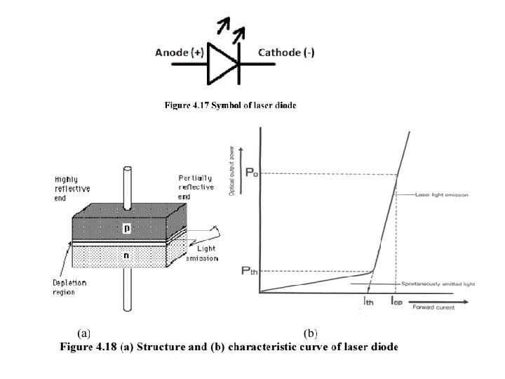

Laser diode theory basics Light absorption: Absorption occurs when light enters a semiconductor and its energy is transferred to the semiconductor to generate additional free electrons and holes Spontaneous emission : The second effect known as spontaneous emission occurs in LEDs. The light produced in this manner is what is termed incoherent Stimulated emission: . A light photon entering the semiconductor lattice will strike an electron and release energy in the form of another light photon The structure of the laser diode creates an optical cavity in which the light photons have multiple reflections
: • photo conductors, photo conductive cells or simply photocells. •")
LDR (LIGHT DEPENDENT RESISTOR): • photo conductors, photo conductive cells or simply photocells. • A photoresistor is made of a high resistance semiconductor. • A Light Dependent Resistor (LDR) or a photo resistor is a device whose resistivity is a function of the incident electromagnetic radiation. Hence, they are light sensitive devices. • A photoresistor or light -dependent resistor (LDR) or photocell is a resistor whose resistance decreases with increasing incident light intensity; in other words, it exhibits photoconductivity.

Working principle of LDR • When light falls i. e. when the photons fall on the device, the electrons in the valence band of the semiconductor material are excited to the conduction band. These photons in the incident light should have energy greater than the band gap of the semiconductor material to make the electrons jump from the valence band to the conduction band. • The result of this process is more and more current starts flowing and hence it is said that the resistance of the device has decreased. This is the most common working principle of LDR

Applications of LDR · used as light sensors. · used when there is a need to detect absences or presences of light like in a camera light meter. · Used in street lamps, alarm clock, burglar alarm circuits, light intensity meters, for counting the packages moving on a conveyor belt, etc. Advantages LDR’s are cheap and are readily available in many sizes and shapes. They need very small power and voltage for its operation. Disadvantages Highly in-accurate with a response time of about tens or hundreds of milliseconds.
- Slides: 16