Analytical Transmissions Electron Microscopy TEM Part I The
- Slides: 49

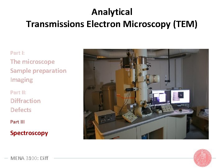
Analytical Transmissions Electron Microscopy (TEM) Part I: The microscope Sample preparation Imaging Part II: Diffraction Defects Part III Spectroscopy MENA 3100: Diff

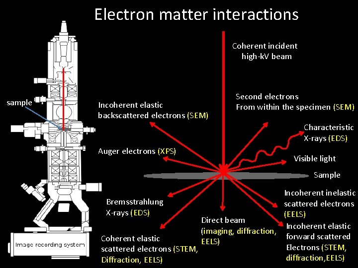
Electron matter interactions Coherent incident high-k. V beam sample Incoherent elastic backscattered electrons (SEM) Second electrons From within the specimen (SEM) Characteristic X-rays (EDS) Auger electrons (XPS) Visible light Sample Incoherent inelastic Bremsstrahlung scattered electrons X-rays (EDS) (EELS) Direct beam Incoherent elastic (imaging, diffraction, forward scattered Coherent elastic EELS) Electrons (STEM, scattered electrons (STEM, diffraction, EELS) Diffraction, EELS)

Energy Dispersive X-ray Spectroscopy (EDS) MENA 3100: Spectroscopy

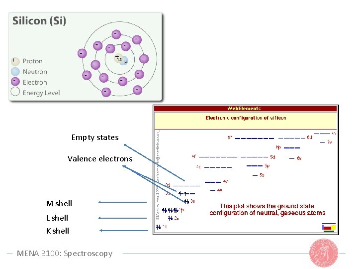
Empty states Valence electrons M shell L shell K shell MENA 3100: Spectroscopy

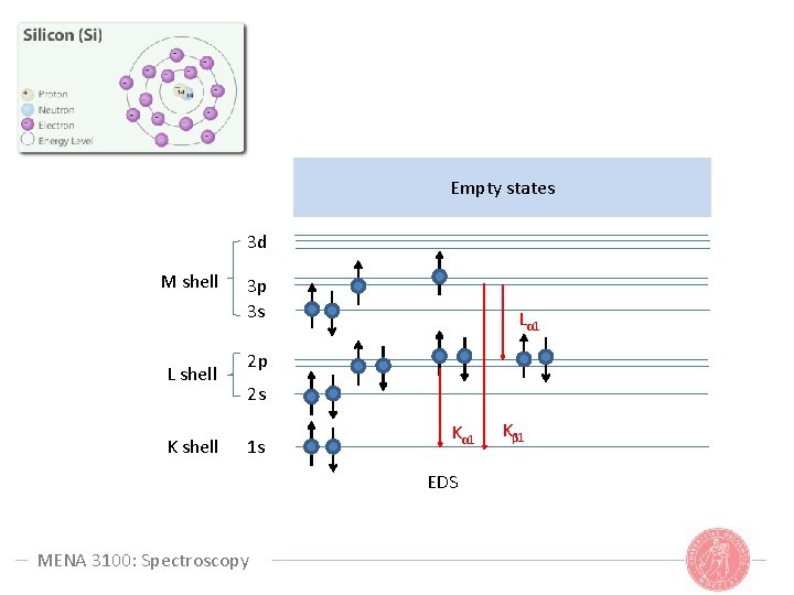
Empty states 3 d M shell L shell K shell 3 p 3 s Lα 1 2 p 2 s 1 s Kα 1 EDS MENA 3100: Spectroscopy Kβ 1

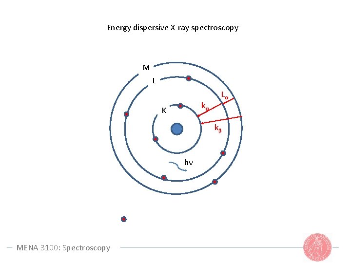
Energy dispersive X-ray spectroscopy M L kα K Lα kβ hν MENA 3100: Spectroscopy

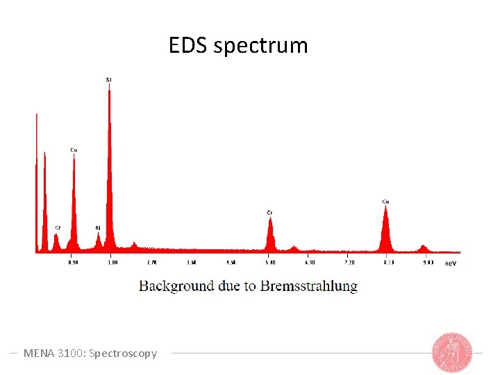
EDS spectrum MENA 3100: Spectroscopy

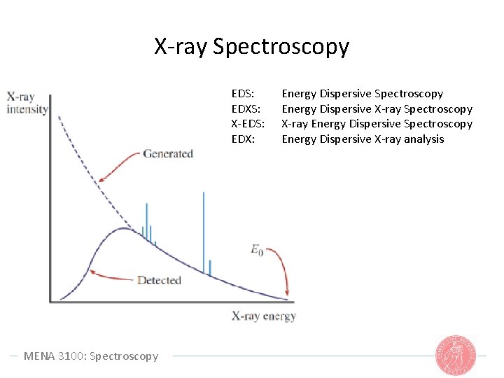
X-ray Spectroscopy EDS: EDXS: X-EDS: EDX: MENA 3100: Spectroscopy Energy Dispersive X-ray Spectroscopy X-ray Energy Dispersive Spectroscopy Energy Dispersive X-ray analysis

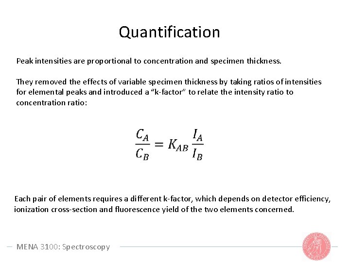
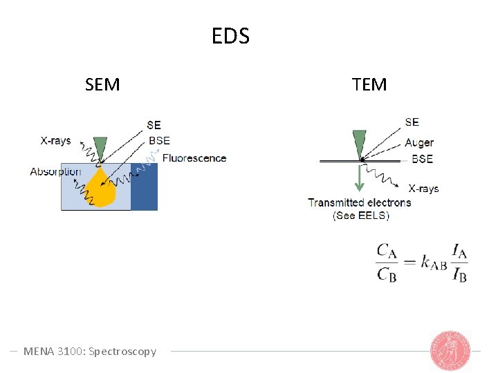
Quantification Peak intensities are proportional to concentration and specimen thickness. They removed the effects of variable specimen thickness by taking ratios of intensities for elemental peaks and introduced a “k-factor” to relate the intensity ratio to concentration ratio: Each pair of elements requires a different k-factor, which depends on detector efficiency, ionization cross-section and fluorescence yield of the two elements concerned. MENA 3100: Spectroscopy

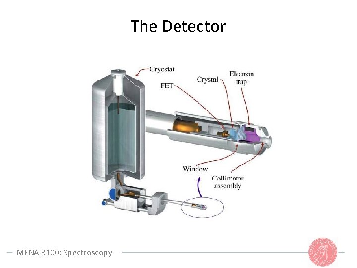
The Detector MENA 3100: Spectroscopy

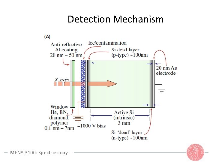
Detection Mechanism MENA 3100: Spectroscopy

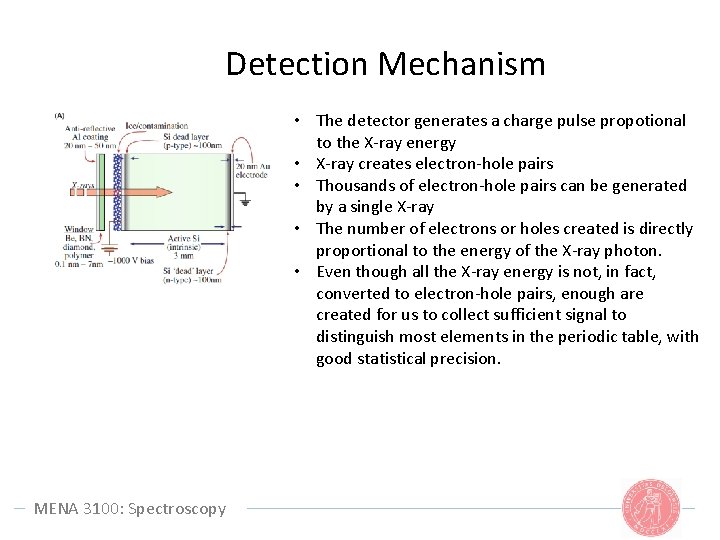
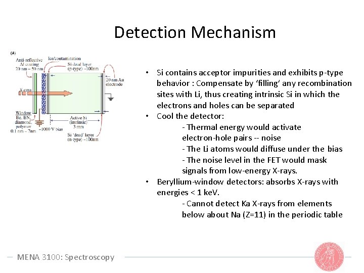
Detection Mechanism • The detector generates a charge pulse propotional to the X-ray energy • X-ray creates electron-hole pairs • Thousands of electron-hole pairs can be generated by a single X-ray • The number of electrons or holes created is directly proportional to the energy of the X-ray photon. • Even though all the X-ray energy is not, in fact, converted to electron-hole pairs, enough are created for us to collect sufficient signal to distinguish most elements in the periodic table, with good statistical precision. MENA 3100: Spectroscopy

Detection Mechanism • Si contains acceptor impurities and exhibits p-type behavior : Compensate by ‘filling’ any recombination sites with Li, thus creating intrinsic Si in which the electrons and holes can be separated • Cool the detector: - Thermal energy would activate electron-hole pairs -- noise - The Li atoms would diffuse under the bias - The noise level in the FET would mask signals from low-energy X-rays. • Beryllium-window detectors: absorbs X-rays with energies < 1 ke. V. - Cannot detect Ka X-rays from elements below about Na (Z=11) in the periodic table MENA 3100: Spectroscopy

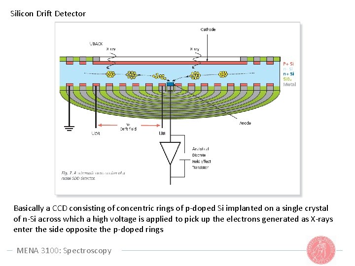
Silicon Drift Detector Basically a CCD consisting of concentric rings of p-doped Si implanted on a single crystal of n-Si across which a high voltage is applied to pick up the electrons generated as X-rays enter the side opposite the p-doped rings MENA 3100: Spectroscopy

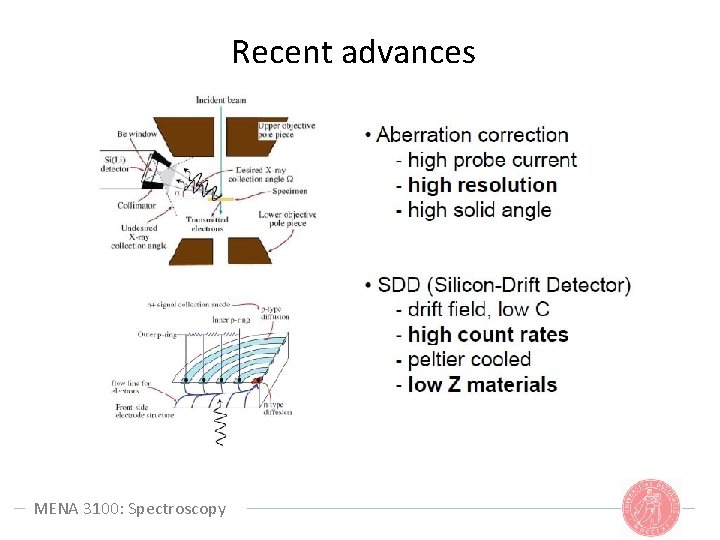
Recent advances MENA 3100: Spectroscopy

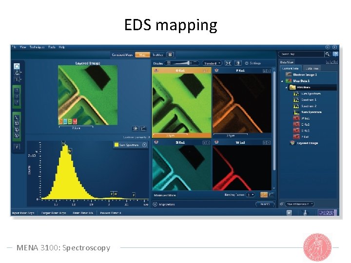
EDS mapping MENA 3100: Spectroscopy

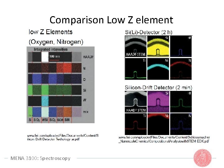
Comparison Low Z element MENA 3100: Spectroscopy

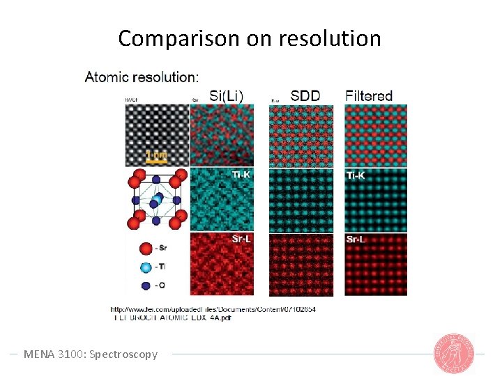
Comparison on resolution MENA 3100: Spectroscopy

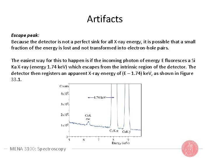
Artifacts Escape peak: Because the detector is not a perfect sink for all X-ray energy, it is possible that a small fraction of the energy is lost and not transformed into electron-hole pairs. The easiest way for this to happen is if the incoming photon of energy E fluoresces a Si Ka X-ray (energy 1. 74 ke. V) which escapes from the intrinsic region of the detector. The detector then registers an apparent X-ray energy of (E – 1. 74) ke. V, as shown in Figure 33. 1. MENA 3100: Spectroscopy

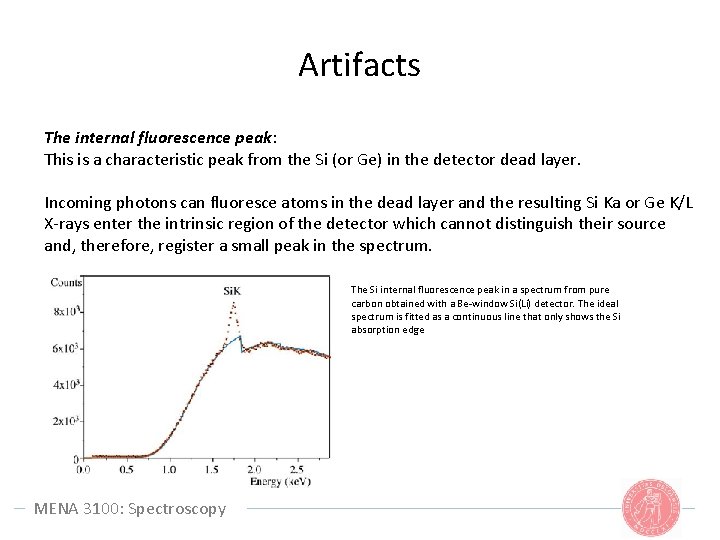
Artifacts The internal fluorescence peak: This is a characteristic peak from the Si (or Ge) in the detector dead layer. Incoming photons can fluoresce atoms in the dead layer and the resulting Si Ka or Ge K/L X-rays enter the intrinsic region of the detector which cannot distinguish their source and, therefore, register a small peak in the spectrum. The Si internal fluorescence peak in a spectrum from pure carbon obtained with a Be-window Si(Li) detector. The ideal spectrum is fitted as a continuous line that only shows the Si absorption edge MENA 3100: Spectroscopy

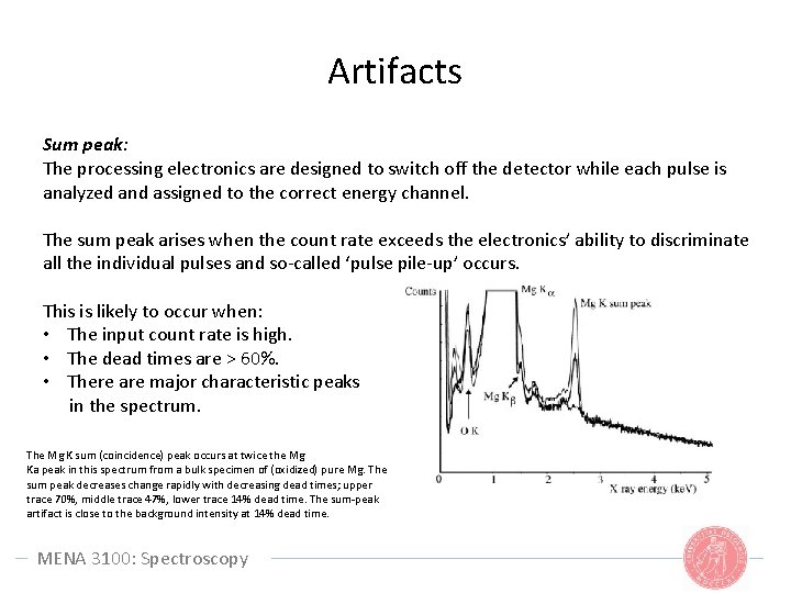
Artifacts Sum peak: The processing electronics are designed to switch off the detector while each pulse is analyzed and assigned to the correct energy channel. The sum peak arises when the count rate exceeds the electronics’ ability to discriminate all the individual pulses and so-called ‘pulse pile-up’ occurs. This is likely to occur when: • The input count rate is high. • The dead times are > 60%. • There are major characteristic peaks in the spectrum. The Mg K sum (coincidence) peak occurs at twice the Mg Ka peak in this spectrum from a bulk specimen of (oxidized) pure Mg. The sum peak decreases change rapidly with decreasing dead times; upper trace 70%, middle trace 47%, lower trace 14% dead time. The sum-peak artifact is close to the background intensity at 14% dead time. MENA 3100: Spectroscopy

EDS SEM MENA 3100: Spectroscopy TEM

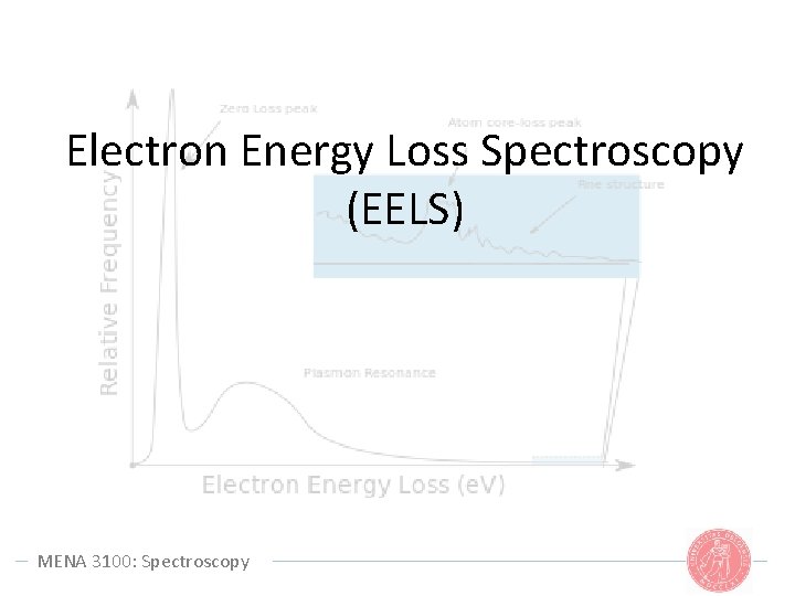
Electron Energy Loss Spectroscopy (EELS) MENA 3100: Spectroscopy

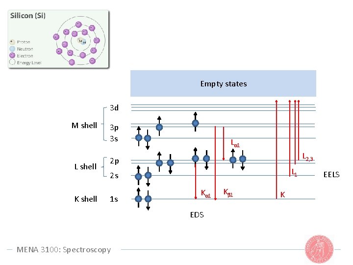
Empty states 3 d M shell L shell K shell 3 p 3 s Lα 1 L 2, 3 2 p L 1 2 s 1 s Kα 1 EDS MENA 3100: Spectroscopy Kβ 1 K EELS

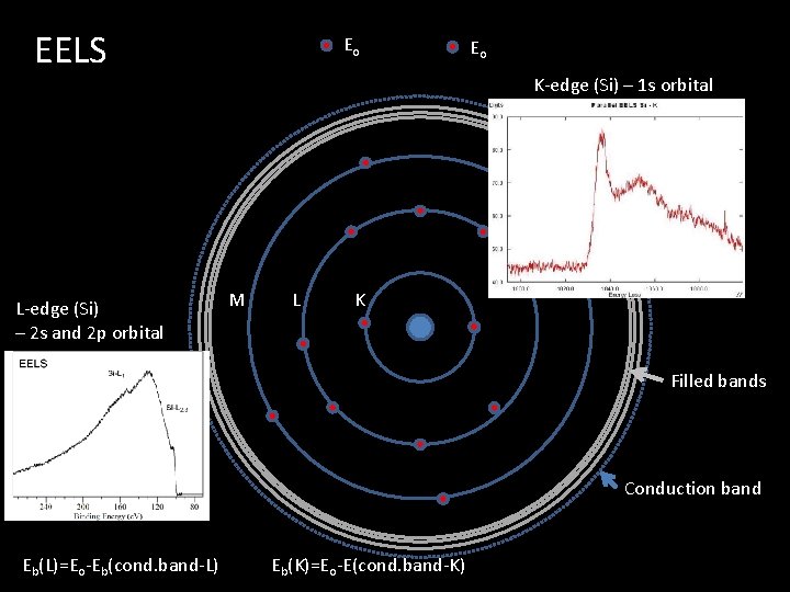
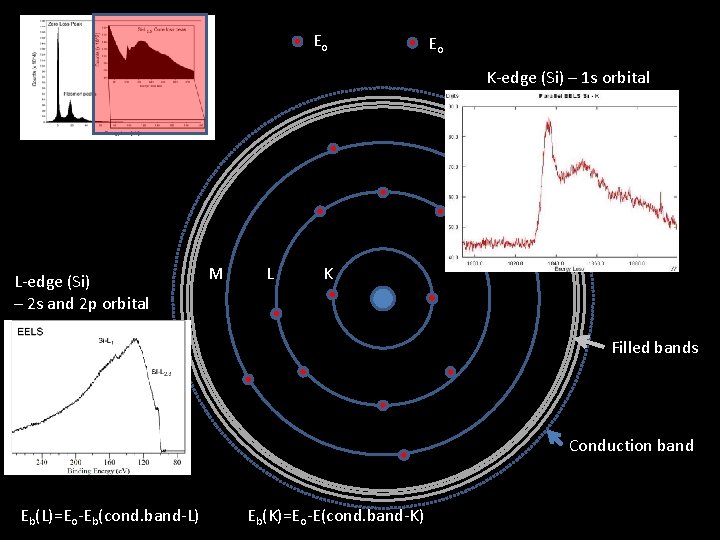
EELS L-edge (Si) – 2 s and 2 p orbital Eo Eo K-edge (Si) – 1 s orbital M L K Filled bands Conduction band Eb(L)=Eo-Eb(cond. band-L) Eb(K)=Eo-E(cond. band-K)

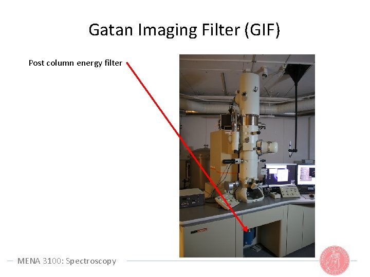
Gatan Imaging Filter (GIF) Post column energy filter MENA 3100: Spectroscopy

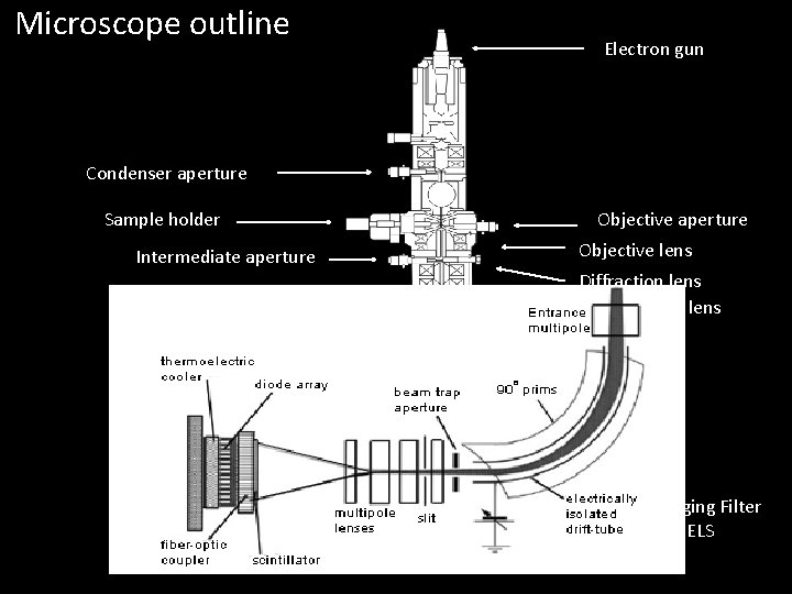
Microscope outline Electron gun Condenser aperture Sample holder Intermediate aperture Projector lenses Objective aperture Objective lens Diffraction lens Intermediate lens Fluorescent screen Gatan Imaging Filter For EELS

MENA 3100: Spectroscopy

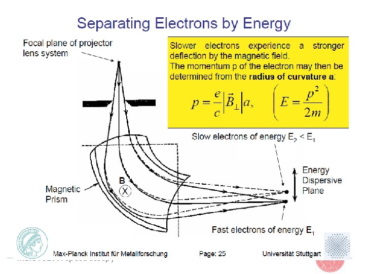
Projector crossover Viewing screen Slit Detector Multipole lenses 90 o magnetic prism Beam trap aperture

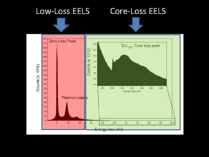
Low-Loss EELS Core-Loss EELS

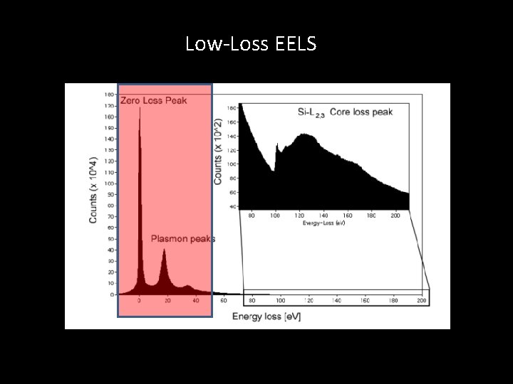
Low-Loss EELS

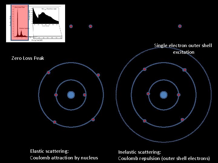
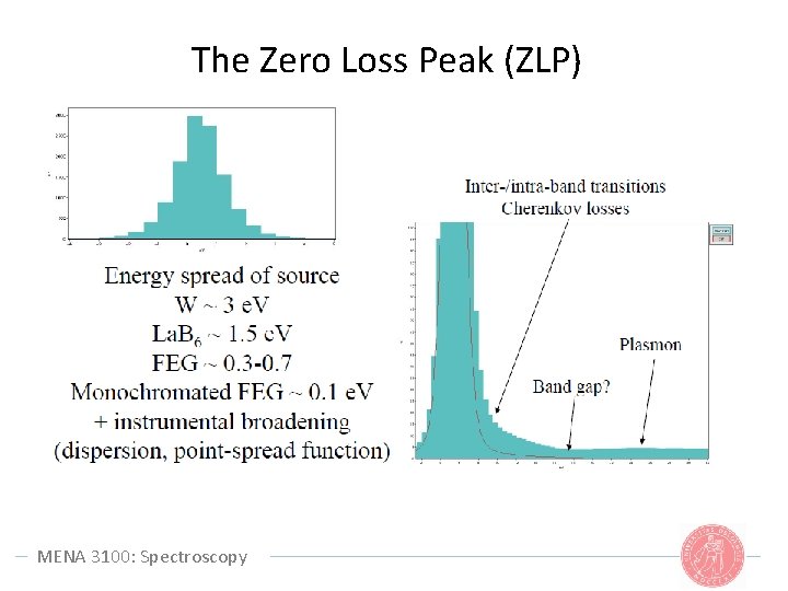
Zero Loss Peak Elastic scattering: Coulomb attraction by nucleus Single electron outer shell excitation Inelastic scattering: Coulomb repulsion (outer shell electrons)

The Zero Loss Peak (ZLP) MENA 3100: Spectroscopy

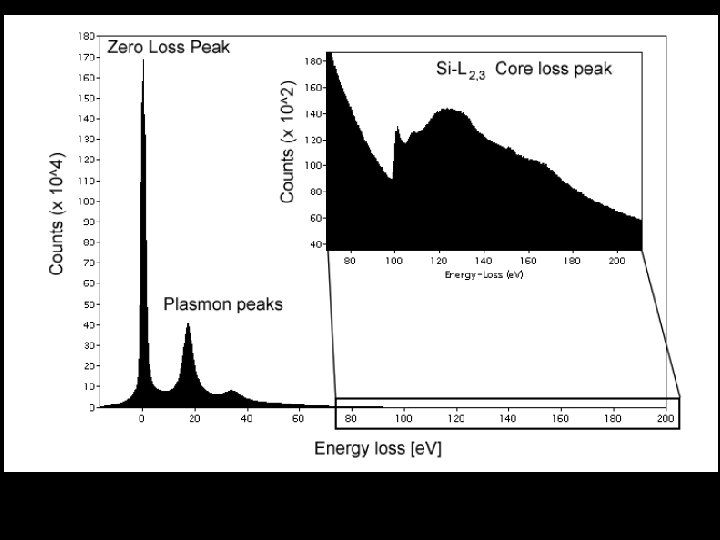
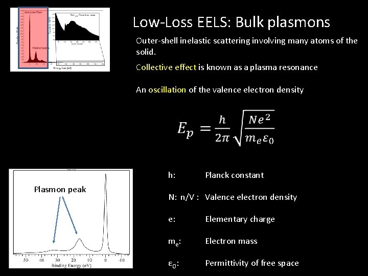
Low-Loss EELS: Bulk plasmons Outer-shell inelastic scattering involving many atoms of the solid. Collective effect is known as a plasma resonance An oscillation of the valence electron density h: Plasmon peak Planck constant N: n/V : Valence electron density e: Elementary charge me: Electron mass εO: Permittivity of free space

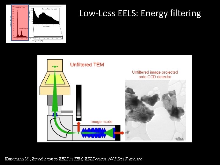
Low-Loss EELS: Energy filtering Kundmann M. , Introduction to EELS in TEM, EELS course 2005 San Francisco

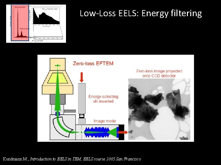
Low-Loss EELS: Energy filtering Kundmann M. , Introduction to EELS in TEM, EELS course 2005 San Francisco

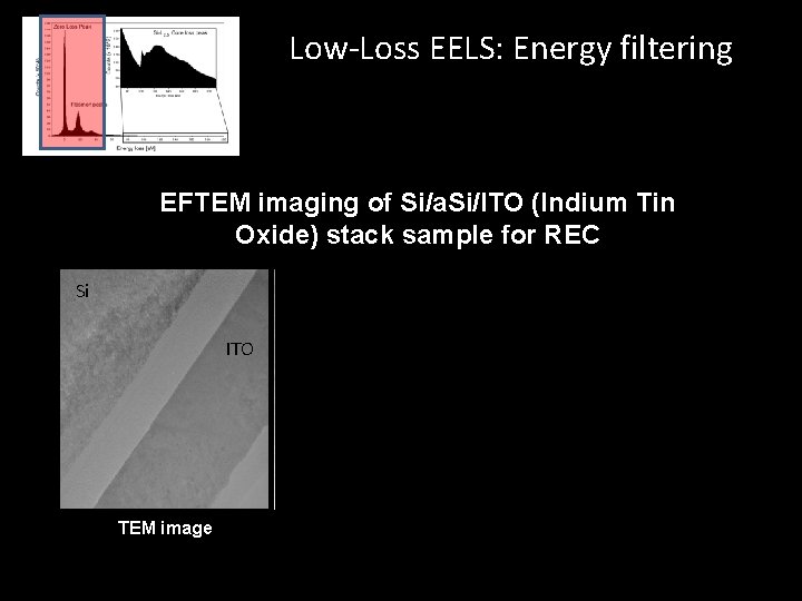
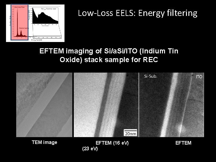
Low-Loss EELS: Energy filtering EFTEM imaging of Si/a. Si/ITO (Indium Tin Oxide) stack sample for REC Si ITO TEM image

Low-Loss EELS: Energy filtering EFTEM imaging of Si/a. Si/ITO (Indium Tin Oxide) stack sample for REC TEM image EFTEM (16 e. V) (23 e. V) EFTEM

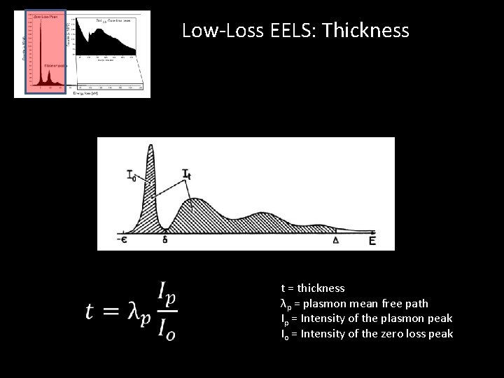
Low-Loss EELS: Thickness t = thickness λp = plasmon mean free path Ip = Intensity of the plasmon peak Io = Intensity of the zero loss peak

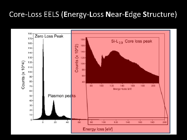
Core-Loss EELS (Energy-Loss Near-Edge Structure)

Eo Eo K-edge (Si) – 1 s orbital L-edge (Si) – 2 s and 2 p orbital M L K Filled bands Conduction band Eb(L)=Eo-Eb(cond. band-L) Eb(K)=Eo-E(cond. band-K)

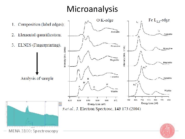
Microanalysis MENA 3100: Spectroscopy

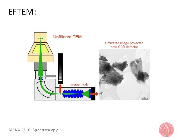
EFTEM: MENA 3100: Spectroscopy

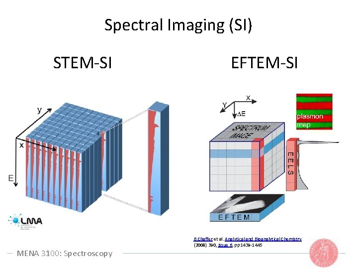
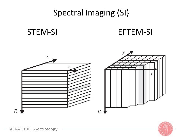
Spectral Imaging (SI) STEM-SI MENA 3100: Spectroscopy EFTEM-SI B. Chaffer et al. Analytical and Bioanalytical Chemistry (2008) 390, Issue 6, pp 1439 -1445

Spectral Imaging (SI) STEM-SI MENA 3100: Spectroscopy EFTEM-SI

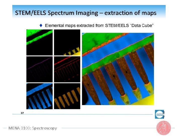
MENA 3100: Spectroscopy

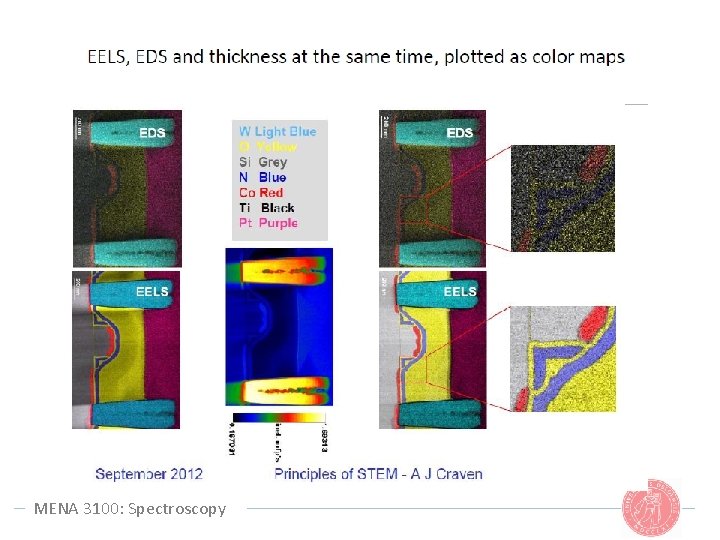
MENA 3100: Spectroscopy

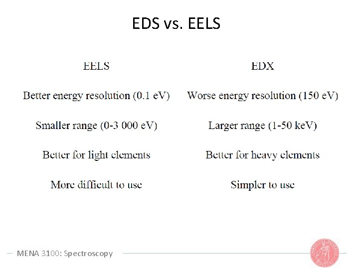
EDS vs. EELS MENA 3100: Spectroscopy

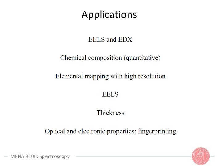
Applications MENA 3100: Spectroscopy