Scanning Electron Microscopy SEM SEM and TEM Scanning
")

 and TEM")
 Scanning electron microscopy is used for inspecting topographies of specimens")
 • The energy of the primary electrons determines the quantity")
 • Backscattered electron imaging is useful in distinguishing one material")


")


 and TEM")


- Slides: 63
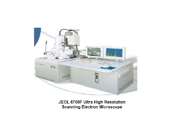
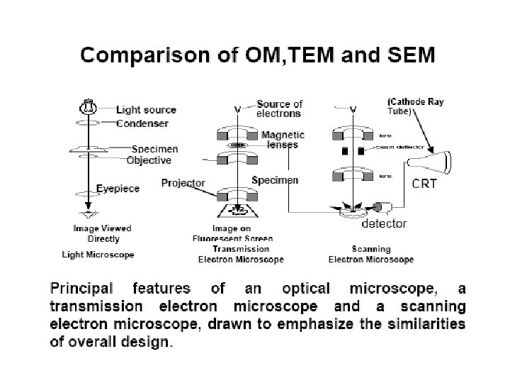
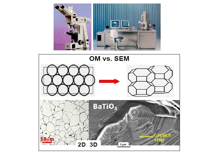
Scanning Electron Microscopy (SEM)
(SEM) and TEM
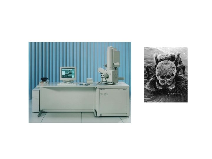
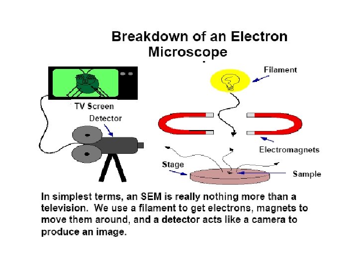
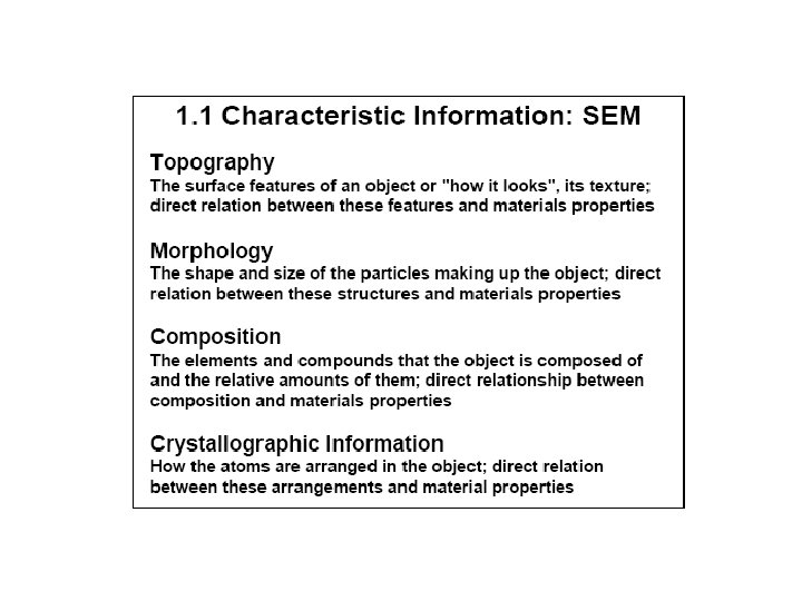
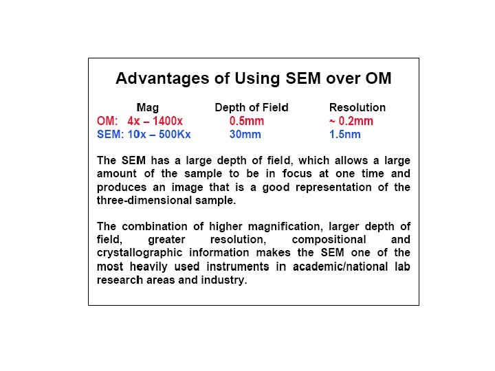
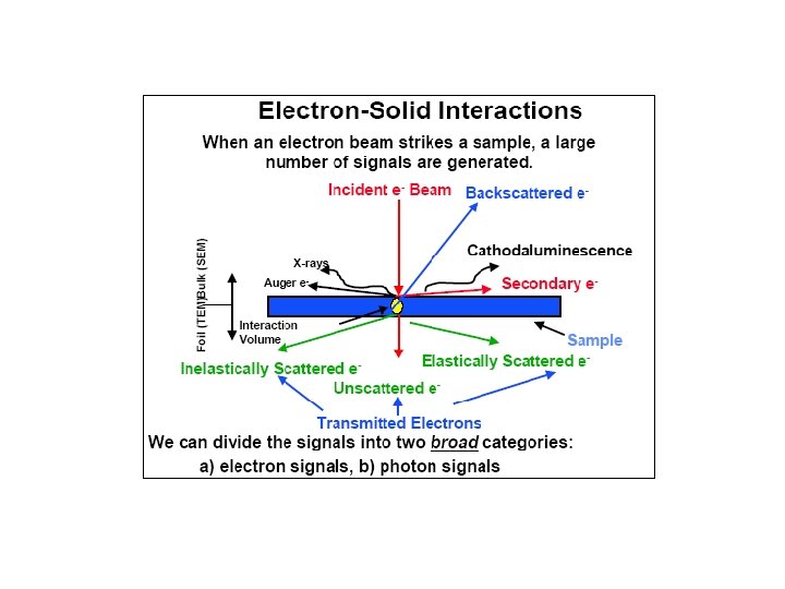
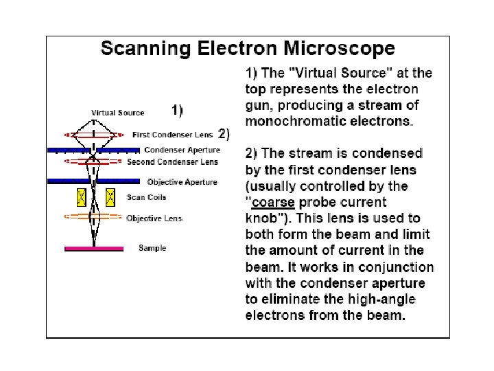
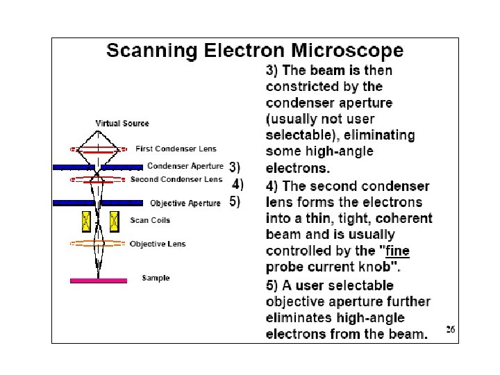
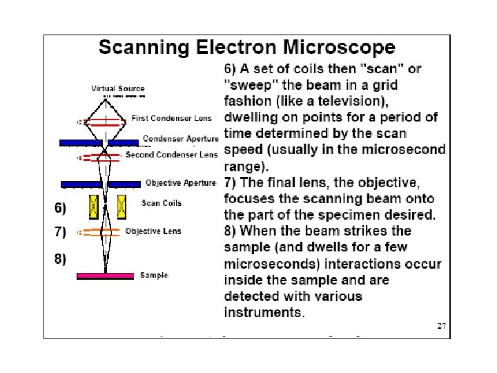
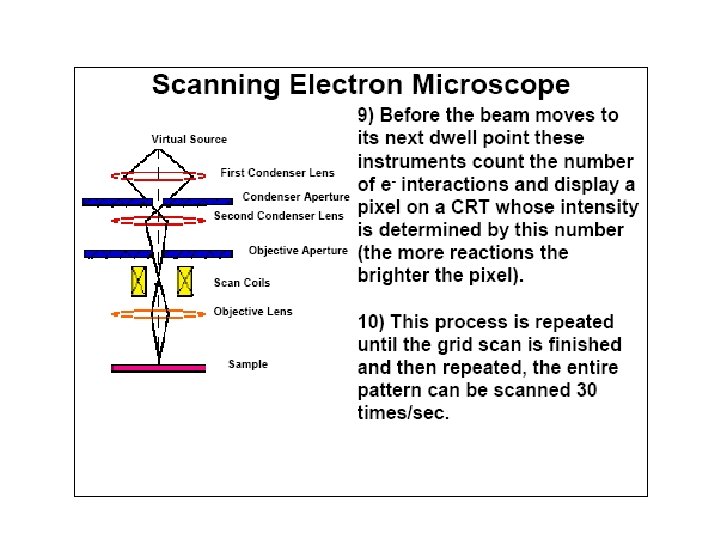
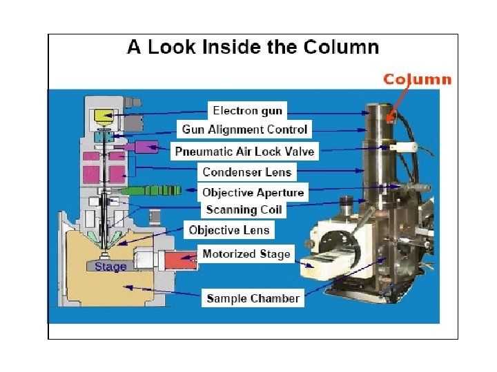
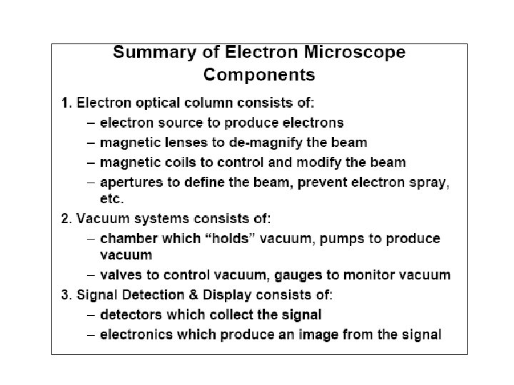
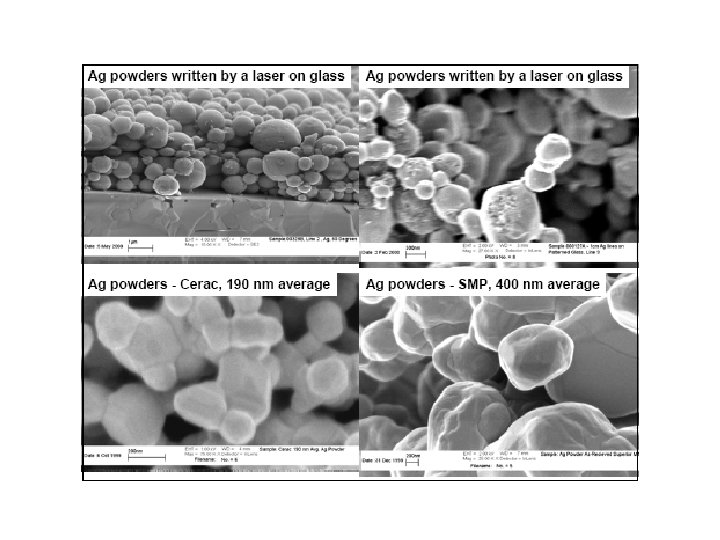
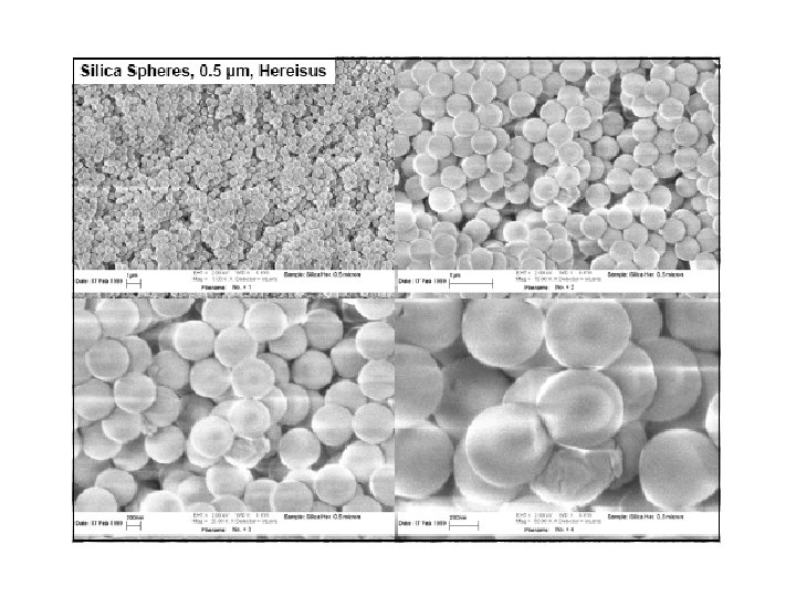
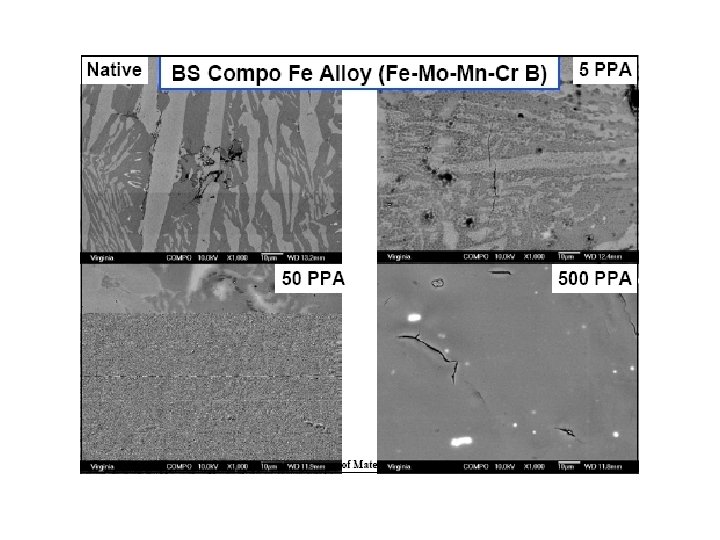
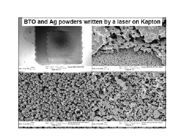
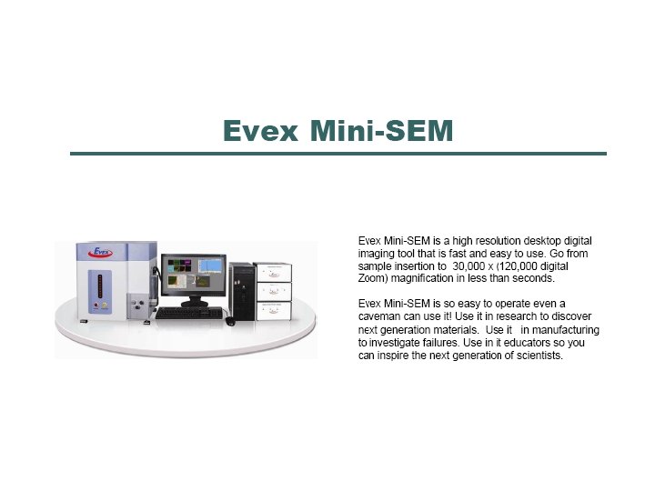
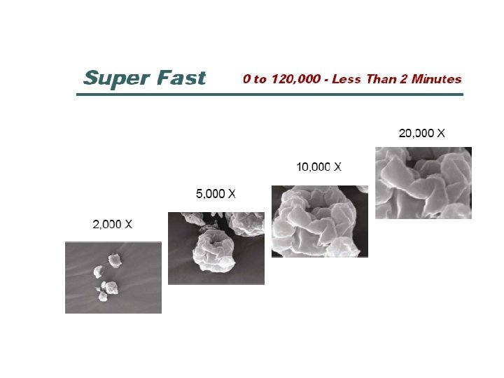
Scanning Electron Microscopy (SEM) Scanning electron microscopy is used for inspecting topographies of specimens at very high magnifications using a piece of equipment called the scanning electron microscope. SEM magnifications can go to more than 300, 000 X but most semiconductor manufacturing applications require magnifications of less than 3, 000 X only. SEM inspection is often used in the analysis of die/package cracks and fracture surfaces, bond failures, and physical defects on the die or package surface. During SEM inspection, a beam of electrons is focused on a spot volume of the specimen, resulting in the transfer of energy to the spot. These bombarding electrons, also referred to as primary electrons, dislodge electrons from the specimen itself. The dislodged electrons, also known as secondary electrons, are attracted and collected by a positively biased grid or detector, and then translated into a signal. To produce the SEM image, the electron beam is swept across the area being inspected, producing many such signals. These signals are then amplified, analyzed, and translated into images of the topography being inspected. Finally, the image is shown on a CRT.
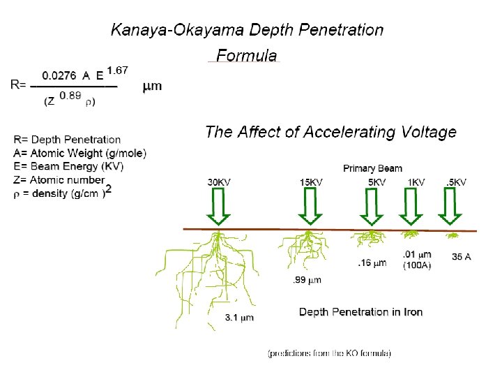
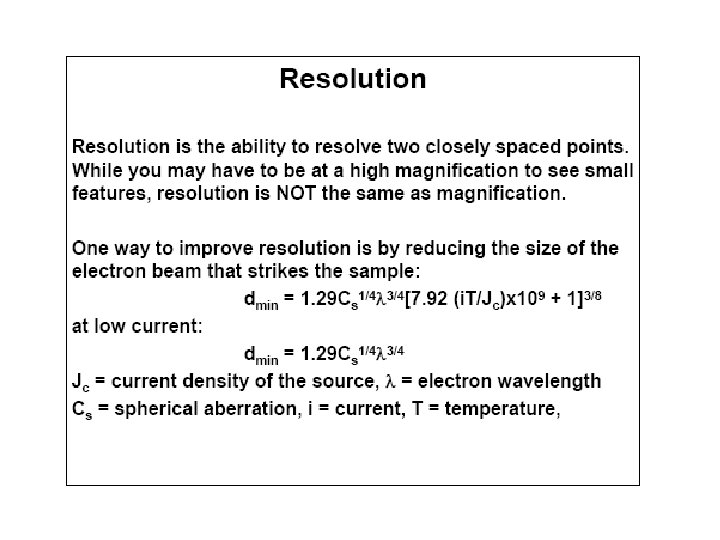
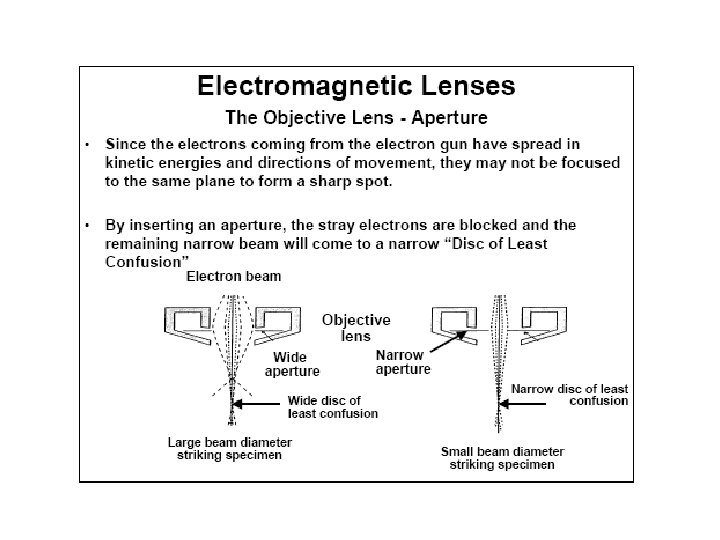
Scanning Electron Microscopy (SEM) • The energy of the primary electrons determines the quantity of secondary electrons collected during inspection. The emission of secondary electrons from the specimen increases as the energy of the primary electron beam increases, until a certain limit is reached. Beyond this limit, the collected secondary electrons diminish as the energy of the primary beam is increased, because the primary beam is already activating electrons deep below the surface of the specimen. Electrons coming from such depths usually recombine before reaching the surface for emission. • • Aside from secondary electrons, the primary electron beam results in the emission of backscattered (or reflected) electrons from the specimen. Backscattered electrons possess more energy than secondary electrons, and have a definite direction. As such, they can not be collected by a secondary electron detector, unless the detector is directly in their path of travel. All emissions above 50 e. V are considered to be backscattered electrons.
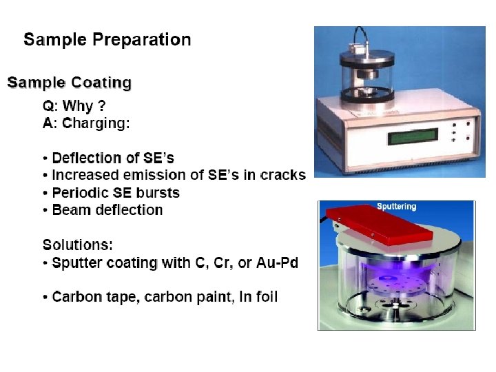
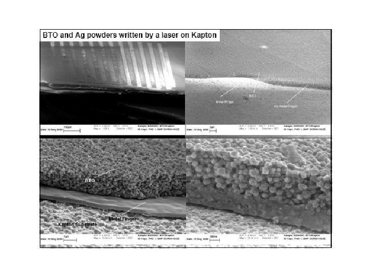
Scanning Electron Microscopy (SEM) • Backscattered electron imaging is useful in distinguishing one material from another, since the yield of the collected backscattered electrons increases monotonically with the specimen's atomic number. Backscatter imaging can distinguish elements with atomic number differences of at least 3, i. e. , materials with atomic number differences of at least 3 would appear with good contrast on the image. For example, inspecting the remaining Au on an Al bond pad after its Au ball bond has lifted off would be easier using backscatter imaging, since the Au islets would stand out from the Al background. • • A SEM may be equipped with an EDX analysis system to enable it to perform compositional analysis on specimens. EDX analysis is useful in identifying materials and contaminants, as well as estimating their relative concentrations on the surface of the specimen.
http: //www. matter. org. uk/tem/default. htm
Electron Microscopy
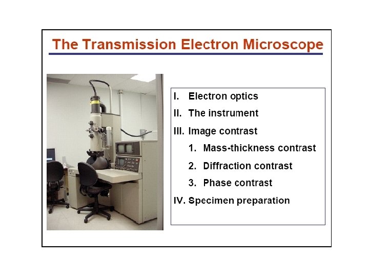
Lecture 5. 2 Transmission Electron Microscopy (TEM)
A transmission Electron Microscope is anologous to a slide projector as indicated by Philips below
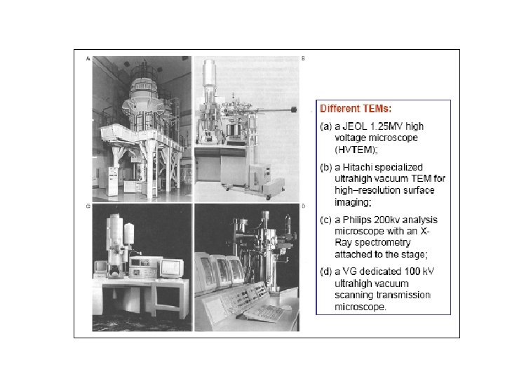
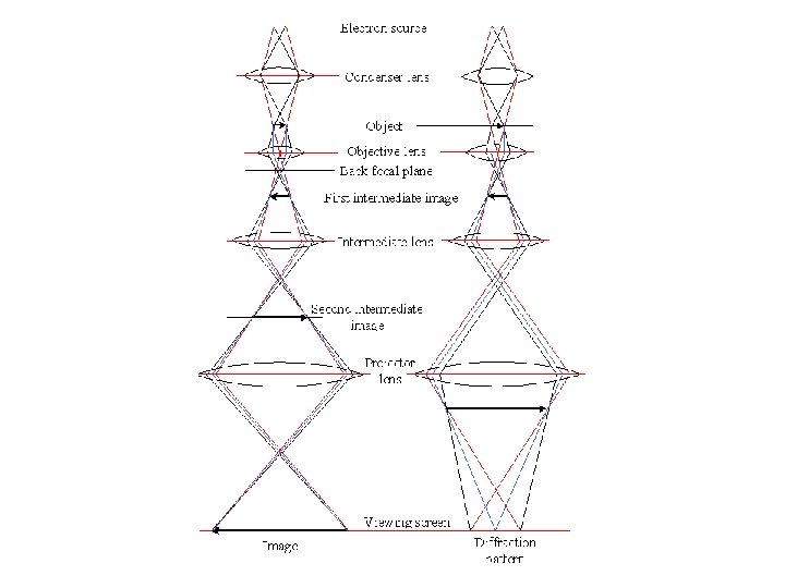
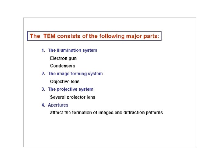
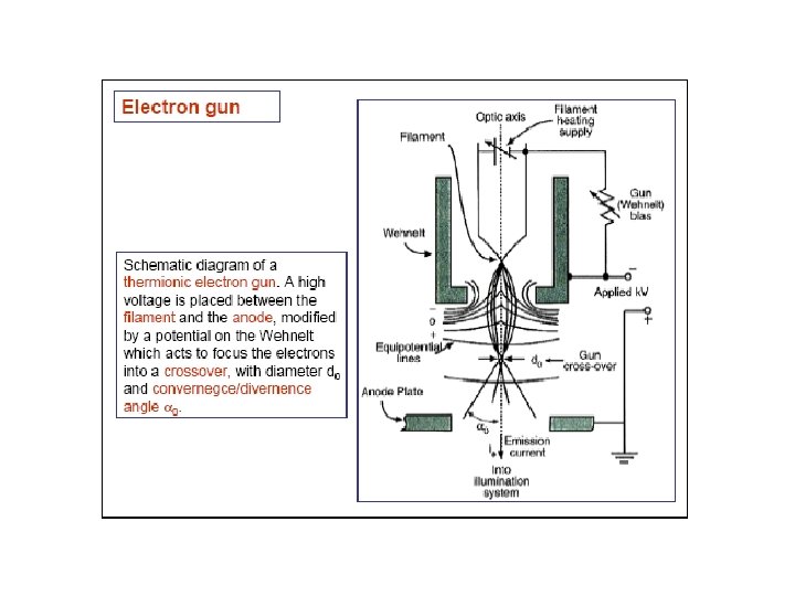
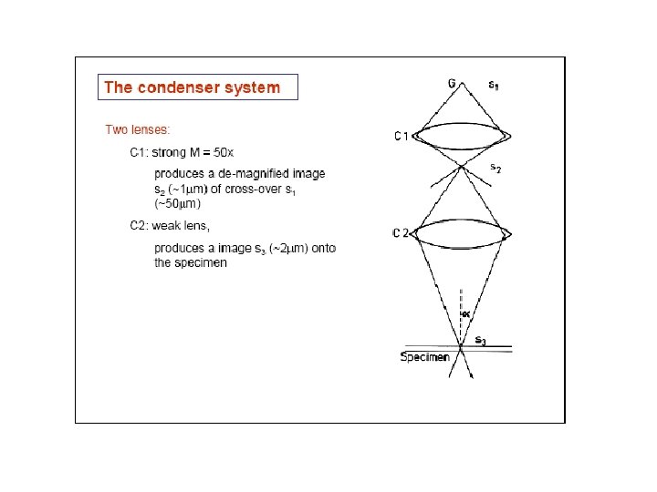
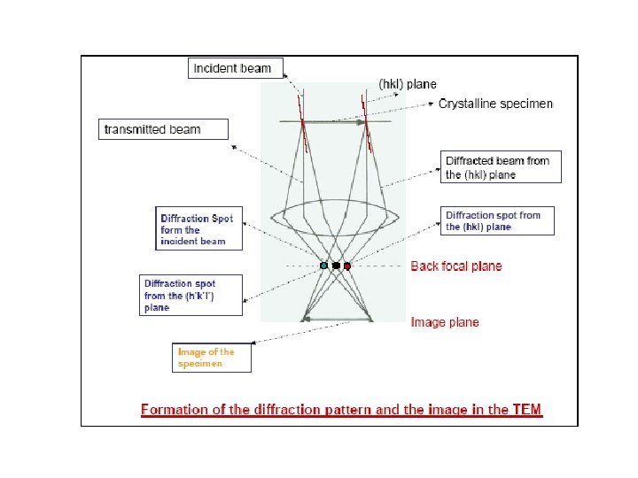
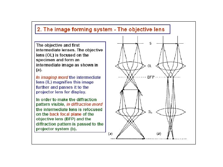
In a conventional transmission electron microscope, a thin specimen is irradiated with an electron beam of uniform current density. Electrons are emitted from the electron gun and illuminate the specimen through a two or three stage condenser lens system. Objective lens provides the formation of either image or diffraction pattern of the specimen. The electron intensity distribution behind the specimen is magnified with a three or four stage lens system and viewed on a fluorescent screen. The image can be recorded by direct exposure of a photographic emulsion or an image plate or digitally by a CCD camera. The acceleration voltage of up to date routine instruments is 120 to 200 k. V. Mediumvoltage instruments work at 200 -500 k. V to provide a better transmission and resolution, and in high voltage electron microscopy (HVEM) the acceleration voltage is in the range 500 k. V to 3 MV. Acceleration voltage determines the velocity, wavelength and hence the resolution (ability to distinguish the neighbouring microstructural features) of the microscope. Depending on the aim of the investigation and configuration of the microscope, transmission electron microscopy can be categorized as : Conventional Transmission Electron Microscopy High Resolution Electron Microscopy Analytical Electron Microscopy Energy-Filtering Electron Microscopy High Voltage Electron Microscopy Dedicated Scanning Transmission Electron Microscopy
(SEM) and TEM
http: //www. matter. org. uk/tem/default. htm
mitochondria