Transmission Electron Microscopy SEM TEM Electron gun Condenser


 q 1 < 10")


- Slides: 45
Transmission Electron Microscopy
SEM & TEM Electron gun Condenser lens Condenser Objective lens Objective Specimen Projector lens Fluorescent screen Specimen Scanning electron microscope Digital camera Transmission electron microscope
Theoretical resolution rth
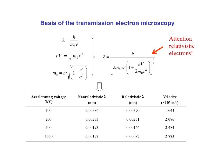
Accelerating voltage Electrons emitted by the filament are accelerated by a series of anodes. For transmission electron microscopy, accelerating voltages typically range from 60 k. V to 300 k. V. Higher accelerating voltages give higher resolution, but less contrast. High accelerating voltages can also result in greater specimen damage. For these reasons, studies of biological samples tend to employ low accelerating voltages (60 k. V to 100 k. V), while studies of inorganic materials, which often require higher resolution, usually employ an accelerating voltage of 200 k. V or more.
Components of the TEM Electrons emitted by the gun are accelerated, typically by 80 - 200 k. V. The condenser lenses focus the beam onto the specimen, which is introduced into the microscope through an airlock. The objective lens forms a focussed image, which is enlarged by the projector lenses. The image is viewed on a fluorescent screen or a computer monitor.
Scheme of beam within a TEM
Electromagnetic lenses All modern TEMs use electromagnetic lenses. These consist of a coil of copper wires inside iron pole pieces. A current through the coils creates a magnetic field, symbolized by red lines in the diagram on the left. Electrons close to the centre are less strongly deflected than those passing through the lens far from the axis.
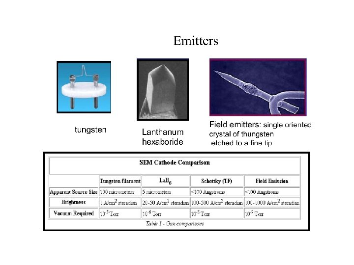
Chromatic aberration is caused by a lens having a different refractive index for different electron energies. It is present in all electron lenses, but can be reduced by minimising the energy spread of the electron source. Field emission sources have the lowest energy spread. There is currently interest in developing chromatic aberration correctors for TEM, but this is still at quite an early stage.
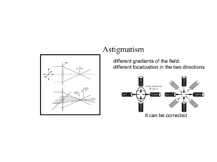
Spherical aberration A lens suffers from spherical aberration if it focuses rays more tightly if they enter it far from the optic axis than if they enter closer to the axis. It therefore does not produce a perfect focal point. This is illustrated in diagram A on the right.
Spherical aberration correctors In recent years, spherical aberration correctors have been developed for transmission electron microscopes, and this has greatly improved their resolving power. Aberration corrected TEMs can have a resolution of 0. 1 nm or better. Using these new ultra-high resolution TEMs it is possible to image the atomic structure of crystals such as graphite, as shown on the right.
Transmission electron microscopy Specimens for TEM 3 mm TEM grid Carbon films
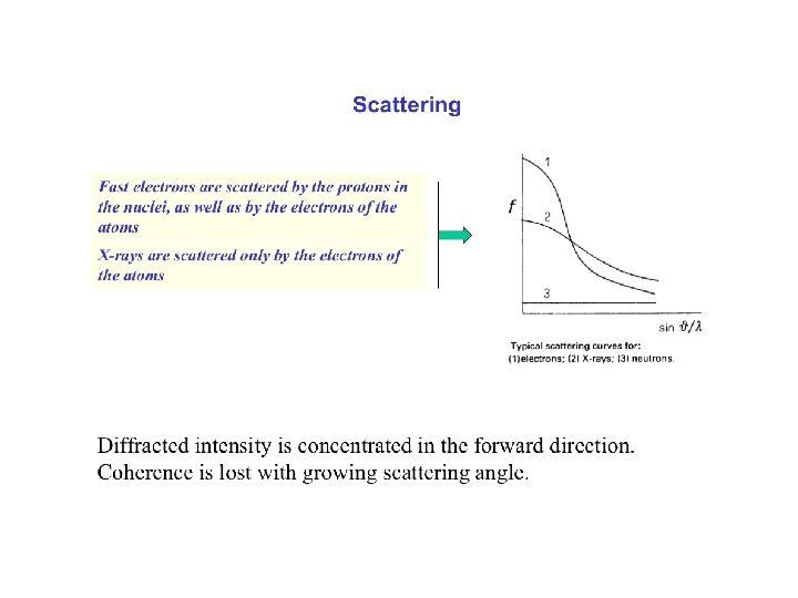
Contrast in the TEM – Scattering Biological and “soft matter” Absorption contrast: Heavy atoms absorb more electrons than light atoms. Scattering contrast: Some electrons blocked by objective aperture.
Positive staining Electron-dense heavy metal salt selectively stains certain features within the sample. Block copolymer containing polystyrene and polymethylmethacrylate stained with ruthenium tetroxide.
Biological TEM - negative staining Surrounding biomolecules with thin amorphous layer of heavy metal salt. Reveals structure, and reduces structural flattening that occurs in the absence of stain. Commonly used stains: uranyl acetate, uranyl formate, sodium/potassium phosphotungstate, ammonium molybdate. Adenovirus negatively stained with uranyl acetate
Biological TEM – preparing specimens from tissue Fix dehydrate set in resin section deposit on grids stain Microtome
Biological TEM – thin section Kidney
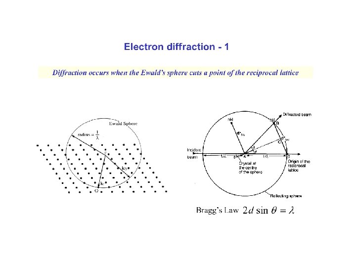
Contrast in the TEM - Diffraction pattern from single crystal Cr 23 C 6 - F cubic a = 10. 659 Å Ni 2 Al. Ti - P cubic a = 2. 92 Å
Contrast in the TEM - Diffraction Polycrystalline materials polycrystalline Ba. Ti. O 3 spotty Debye rings
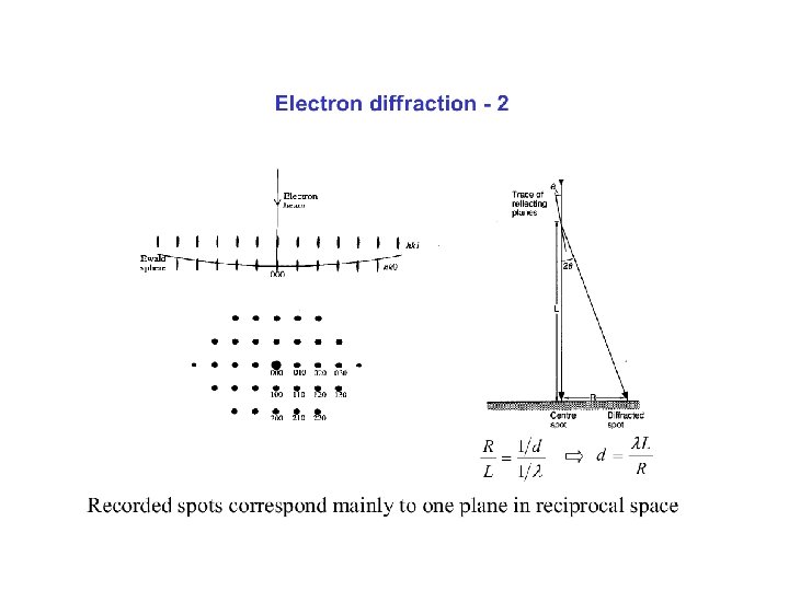
Contrast in the TEM - 2 Diffraction contrast
Bright Field Imaging • If the main portion of the near-forward scattered beam is used to form the image • transmitted beam • 000 beam • zero-order beam
Transmission electron microscopy TEM in physical science – bright field imaging Dislocations in stainless steel foil Platinum/alumina catalyst
Ray Paths in the TEM
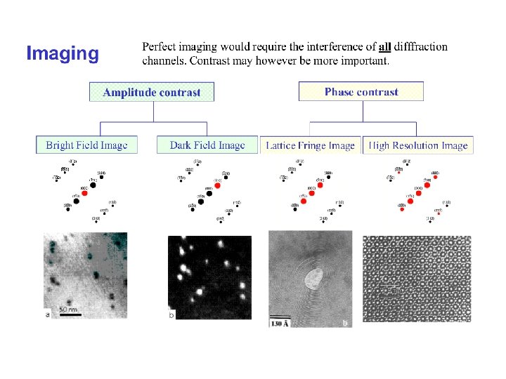
Electron Diffraction TEM Imaging Modes: Diffraction vs BF
Dark Field Imaging • If the transmitted beam is excluded from the image formation process • off-axis imaging • tilted beam imaging
TEM Imaging: Ray Paths
Contrast in the TEM - 3 Phase contrast: lattice imaging
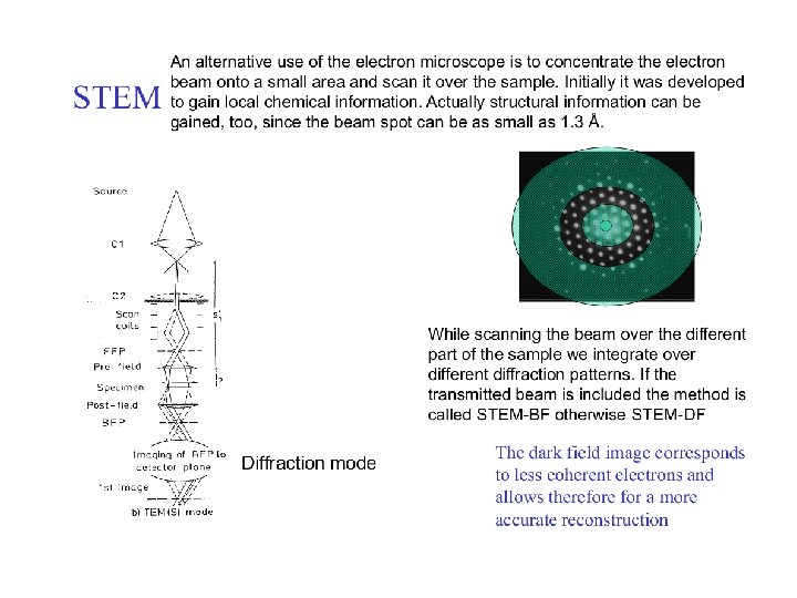
High Angular Annular Dark Field Scattered intensity = f(Z 2) q 1 < 10 mrad Transmetted electrons q 2 10 – 50 mrad Diffracted electrons q 3 > 50 mrad Scattered electrons HAADF detector is highly sensitive to heavy atoms
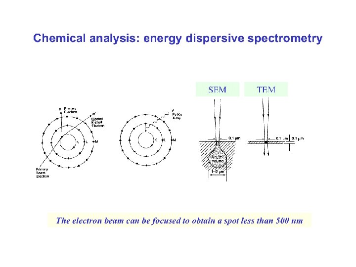
Energy Dispersed Spectroscopy
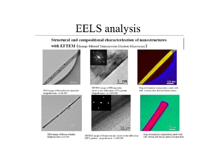
Electron Energy Loss Spectroscopy - EELS -