9 Memory ROM kuic kyonggi ac krdssung 9

의 특성 ROM이란 읽기 전용의 기억소자로")


. Pin Configuration NOR Flash Memory Address [ A 21")
![kuic. kyonggi. ac. kr/~dssung A[MAX: 0] – 8 Mbit : MAX = 18 16](https://slidetodoc.com/presentation_image_h/a90d75087d3ce8a14e2f752b86d22333/image-16.jpg "kuic. kyonggi. ac. kr/~dssung A[MAX: 0] – 8 Mbit : MAX = 18 16")
. Block Size Device is asymmetrically blocked main block (32")


. Read Operation Address CE# OE# WE# Data")
. Write Operation Address CE# OE# WE# Data")
. Read Array RP# low to high transition -> and")
. Read Status Register Read Status Command (0 x 70)")
. Block Erase / Confirm Two-Cycle Sequence Erase Setup Command")

. Program Two-Cycle Sequence Program Setup Command (0 x 40)")


. Pin Configuration NAND Flash Memory I/O [ I/O 15")
 - Data/Address/Command multiplexed I/O port")
 ALE (Address Latch Enable) Command Latch")
. Functional Block Diagram 256 M X 8 bit NAND")
를 위한 spare area - Hamming code")


. Basic Timing Diagram CLE (Command Latch Enable) ALE (Address")


![kuic. kyonggi. ac. kr/~dssung SR[6] => 1: Ready 0: Busy SR[0] => 1: Fail](https://slidetodoc.com/presentation_image_h/a90d75087d3ce8a14e2f752b86d22333/image-42.jpg "kuic. kyonggi. ac. kr/~dssung SR[6] => 1: Ready 0: Busy SR[0] => 1: Fail")

. Read")

. Erase t. BERS : 2 ms Only address A")

. Program t. PROG : 300 usec")

- Slides: 49
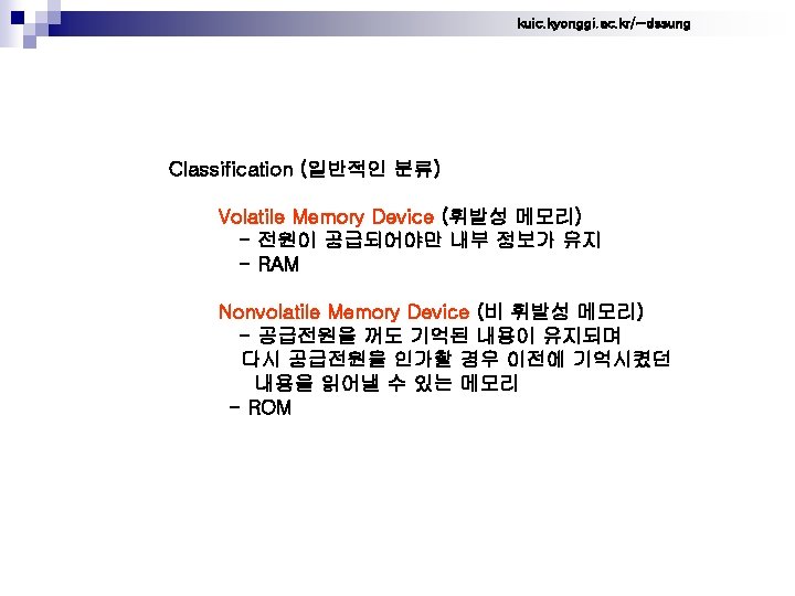
제 9장 Memory - ROM
kuic. kyonggi. ac. kr/~dssung 9. 1 ROM (Read-Only Memory)의 특성 ROM이란 읽기 전용의 기억소자로 CPU가 임의적으로 Write할 수 없다. - ROM, PROM, EPROM 전원이 없어도 정보를 유지한다 = Nonvolatile Memory ROM (Nonprogrammable Read-Only Memory) PROM (Programmable, nonerasable, ROM) UV EPROM (Ultra. Violet Erasable, Programmable ROM) EEPROM (Electrically Erasable PROM) Flash memory
kuic. kyonggi. ac. kr/~dssung ROM Address Data CE# Chip Enable OE# Output Enable Vcc GND
kuic. kyonggi. ac. kr/~dssung Address CE# OE# Data
kuic. kyonggi. ac. kr/~dssung EEROM Data Address Ready/Busy CE# Chip Enable OE# Output Enable WE# Write Enable RDY/BUSY# Vcc GND
kuic. kyonggi. ac. kr/~dssung 9. 6 Flash memory - can be erased in units of memory called blocks initially, overall erase -> flash - EEPROM와 비교하여 Flash memory의 장점 : cell의 크기 -> lower cost and available in higher densities EEPROM의 경우 cell단위의 독립적인 erasing을 위하여 TR 한 개 추가 -> memory updating is faster flash : erasing과 programming의 독립 EEPROM : erasing과 programming이 연속 진행 단점 : byte단위의 정보 지움이 불가능 -> flash는 block단위의 지움만 가능 -> flash의 경우 writing시 정보가 overwriting ex) 0 x. F 0 writing -> 0 x 0 F writing : result => 0 x 00 1: x->x, 0: x->0 -> EEPROM의 경우 ex) 0 x. F 0 writing -> 0 x 0 F writing : result => 0 x 0 F
kuic. kyonggi. ac. kr/~dssung
kuic. kyonggi. ac. kr/~dssung 9. 7 Intel NOR Flash Memory - 8 Mbit, 16 Mbit, 32 Mbit, 64 Mbit (1). 특성 - block size : 4 Kword, 32 Kword - random read : 70 nsec – 100 nsec serial access : 70 nsec – 100 nsec program time : 0. 1 sec/4 Kword, 0. 8 sec/32 Kword block erase time : 0. 5 sec/4 Kword, 1 sec/32 Kword
kuic. kyonggi. ac. kr/~dssung (2). Pin Configuration NOR Flash Memory Address [ A 21 - A 0 ] Data [ D 15 - D 0 ] CE# Chip Enable OE# Output Enable WE# Write Enable Vpp RP# Vcc WP# Write Protect GND
kuic. kyonggi. ac. kr/~dssung A[MAX: 0] – 8 Mbit : MAX = 18 16 Mbit : MAX = 19 32 Mbit : MAX = 20 64 Mbit : MAX = 21 WP# : Write Protect RP# : Reset/Deep power down low -> drives the outputs to high-Z, resets internal states minimizes current level low to high transition -> resets all blocks to locked and defaults to the read array mode Vpp : Program/Erase Power Supply
kuic. kyonggi. ac. kr/~dssung (3). Block Size Device is asymmetrically blocked main block (32 K word) - code or (initialized) data boot block (4 K word) - boot code or frequently changing small parameters - 적은 용량 : block의 낭비 방지 - 적은 용량 : 빠른 erase time - 적은 용량 : 많은 block erase cycling block error (block내 문제 있는 bit가 존재) 의 확률이 낮아짐
kuic. kyonggi. ac. kr/~dssung
kuic. kyonggi. ac. kr/~dssung
kuic. kyonggi. ac. kr/~dssung (4). Read Operation Address CE# OE# WE# Data
kuic. kyonggi. ac. kr/~dssung (5). Write Operation Address CE# OE# WE# Data
kuic. kyonggi. ac. kr/~dssung (6). Read Array RP# low to high transition -> and defaults to the read array mode If the device is not in read array mode, Read Array Command (0 x. FF) must be issued Read array mode에서 연속적인 메모리 읽기 가능
kuic. kyonggi. ac. kr/~dssung (7). Read Status Register Read Status Command (0 x 70) causes subsequent reads to output data from the status register until another command is issued Status register bits are output on DQ[7: 0] SR[7] : Write State Machine Status 1: Ready 0: Busy SR[5] : Erase Status 1: Error In Block Erase 0: Successful Block Erase SR[4] : Program Status 1: Error In Programming 0: Successful Programming
kuic. kyonggi. ac. kr/~dssung (8). Block Erase / Confirm Two-Cycle Sequence Erase Setup Command (0 x 20) Erase Confirm (0 x. D 0) After this command, default to Read Status Mode
kuic. kyonggi. ac. kr/~dssung Write Address : block address Data : 0 x 20 Write Address : block address Data : 0 x. D 0 Read (Status Register) Address : don’t care Data : SR SR[7] 1 SR[5] 0 block erase complete 0 1 block erase error
kuic. kyonggi. ac. kr/~dssung (9). Program Two-Cycle Sequence Program Setup Command (0 x 40) Address and Data to be programmed After this command, default to Read Status Mode
kuic. kyonggi. ac. kr/~dssung Write Address : word address Data : 0 x 40 Write Address : word address Data : data Read (Status Register) Address : don’t care Data : SR SR[7] 1 SR[4] 0 program complete 0 1 program error
kuic. kyonggi. ac. kr/~dssung 9. 8 SAMSUNG 2 Gbit NAND Flash Memory - 256 M X 8 bit NAND Flash Memory - 128 M X 16 bit NAND Flash Memory (1). 특성 - Data/Address/Command multiplexed I/O port - page size : 2 K byte - block size : 128 K byte - random read : 25 usec serial access : 50 nsec, 80 nsec program time : 300 usec block erase time : 2 ms
kuic. kyonggi. ac. kr/~dssung (2). Pin Configuration NAND Flash Memory I/O [ I/O 15 – I/O 0 ] I/O [ I/O 7 – I/O 0 ] Vcc GND PRE CE# RE# WP# ALE CLE R/B#
kuic. kyonggi. ac. kr/~dssung I/O (Data Input / Output) - Data/Address/Command multiplexed I/O port page 단위로 정보를 교환하기 때문에 초기 address만 필요 CE# (Chip Enable) RE# (Read Enable) – falling edge WE# (Write Enable) – rising edge CLE (Command Latch Enable) ALE (Address Latch Enable) R/B# (Ready / Busy Output) WP# (Write Protect) : Hardware data protection - write & erase protect PRE (Power-on Read Enable) : Power-On Auto-Read operation - power on 시 자동으로 첫 번째 block의 read mode
kuic. kyonggi. ac. kr/~dssung CLE (Command Latch Enable) ALE (Address Latch Enable) Command Latch : CLE = 1, ALE = 0 I/O port가 Command 입력으로 이용 CE# = 0, RE# = 1, WE# = 0 Address Latch : CLE = 0, ALE = 1 I/O port가 Address 입력으로 이용 CE# = 0, RE# = 1, WE# = 0 Status Output, Data Input, Output : CLE = 0, ALE = 0 I/O port가 Status 출력 또는 Data 입출력으로 이용
kuic. kyonggi. ac. kr/~dssung (3). Functional Block Diagram 256 M X 8 bit NAND Flash Memory
kuic. kyonggi. ac. kr/~dssung ECC (Error Correcting Code)를 위한 spare area - Hamming code (1 bit correction & 2 bit detection)
kuic. kyonggi. ac. kr/~dssung
kuic. kyonggi. ac. kr/~dssung 128 M X 16 bit NAND Flash Memory
kuic. kyonggi. ac. kr/~dssung
kuic. kyonggi. ac. kr/~dssung
kuic. kyonggi. ac. kr/~dssung (4). Basic Timing Diagram CLE (Command Latch Enable) ALE (Address Latch Enable) Command Latch : CLE = 1, ALE = 0 I/O port가 Command 입력으로 이용 CE# = 0, RE# = 1, WE# = 0 Address Latch : CLE = 0, ALE = 1 I/O port가 Address 입력으로 이용 CE# = 0, RE# = 1, WE# = 0 Status Output, Data Input, Output : CLE = 0, ALE = 0 I/O port가 Status 출력 또는 Data 입출력으로 이용
kuic. kyonggi. ac. kr/~dssung
kuic. kyonggi. ac. kr/~dssung
kuic. kyonggi. ac. kr/~dssung
kuic. kyonggi. ac. kr/~dssung SR[6] => 1: Ready 0: Busy SR[0] => 1: Fail 0: Pass
kuic. kyonggi. ac. kr/~dssung
kuic. kyonggi. ac. kr/~dssung (5). Read
kuic. kyonggi. ac. kr/~dssung t. R : 25 usec, t. RC : 50 nsec, 80 nsec
kuic. kyonggi. ac. kr/~dssung (6). Erase t. BERS : 2 ms Only address A 18 to A 28(X 8) or A 17 to A 27(X 16) is valid while A 12 to A 17(X 8) or A 11 to A 16(X 16) is ignored
kuic. kyonggi. ac. kr/~dssung
kuic. kyonggi. ac. kr/~dssung (7). Program t. PROG : 300 usec
kuic. kyonggi. ac. kr/~dssung