Memory Devices Read Only Memory ROM Structure of

- Slides: 34

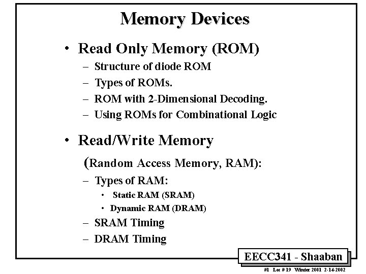
Memory Devices • Read Only Memory (ROM) – – Structure of diode ROM Types of ROMs. ROM with 2 -Dimensional Decoding. Using ROMs for Combinational Logic • Read/Write Memory (Random Access Memory, RAM): – Types of RAM: • Static RAM (SRAM) • Dynamic RAM (DRAM) – SRAM Timing – DRAM Timing EECC 341 - Shaaban #1 Lec # 19 Winter 2001 2 -14 -2002

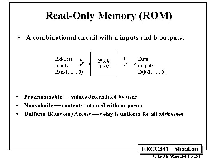
Read-Only Memory (ROM) • A combinational circuit with n inputs and b outputs: Address n inputs A(n-1, . . . , 0) 2 n x b ROM b Data outputs D(b-1, . . . , 0) • Programmable ¾ values determined by user • Nonvolatile ¾ contents retained without power • Uniform (Random) Access ¾ delay is uniform for all addresses EECC 341 - Shaaban #2 Lec # 19 Winter 2001 2 -14 -2002

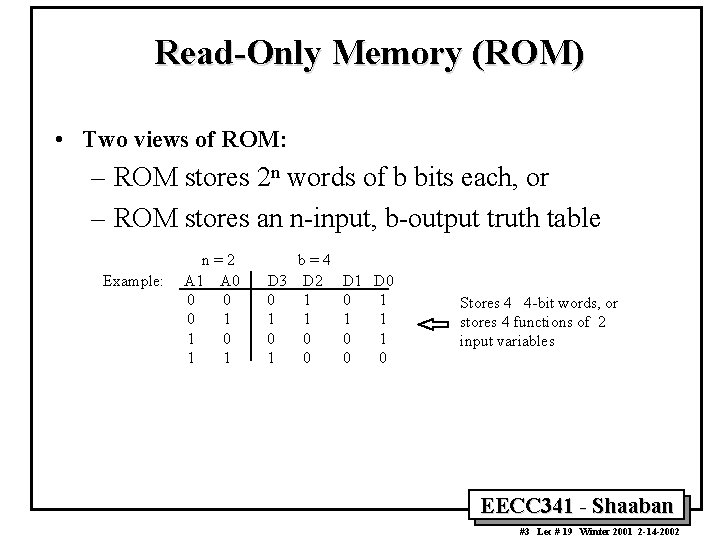
Read-Only Memory (ROM) • Two views of ROM: – ROM stores 2 n words of b bits each, or – ROM stores an n-input, b-output truth table Example: n=2 A 1 A 0 0 1 1 b=4 D 3 D 2 0 1 1 1 0 0 1 0 D 1 D 0 0 1 1 1 0 0 Stores 4 4 -bit words, or stores 4 functions of 2 input variables EECC 341 - Shaaban #3 Lec # 19 Winter 2001 2 -14 -2002

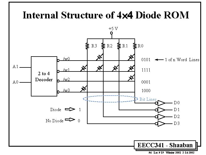
Internal Structure of 4´ 4 Diode ROM +5 V R 3 A 1 A 0 2 to 4 Decoder R 2 R 1 R 0 /w 0 0101 /w 1 1111 /w 2 1 of n Word Lines 0001 /w 3 1000 Bit Lines Diode 1 No Diode 0 D 1 D 2 D 3 EECC 341 - Shaaban #4 Lec # 19 Winter 2001 2 -14 -2002

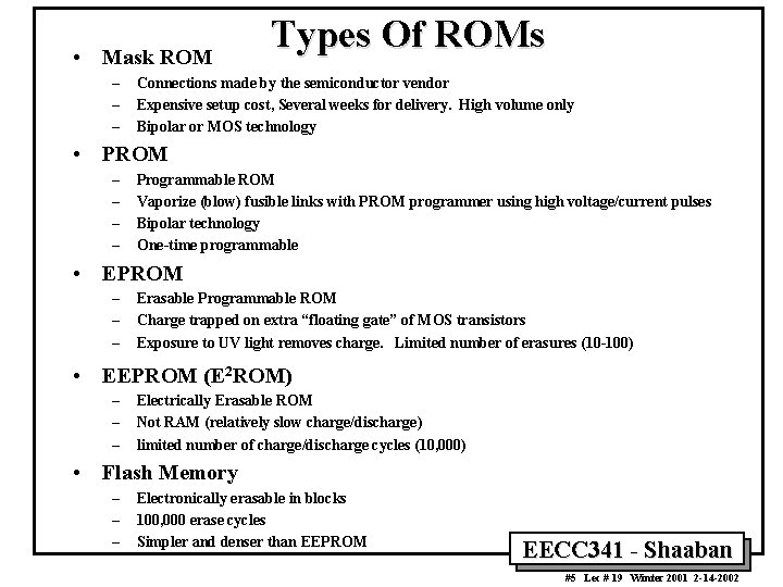
• Mask ROM – – – Types Of ROMs Connections made by the semiconductor vendor Expensive setup cost, Several weeks for delivery. High volume only Bipolar or MOS technology • PROM – – Programmable ROM Vaporize (blow) fusible links with PROM programmer using high voltage/current pulses Bipolar technology One-time programmable • EPROM – – – Erasable Programmable ROM Charge trapped on extra “floating gate” of MOS transistors Exposure to UV light removes charge. Limited number of erasures (10 -100) • EEPROM (E 2 ROM) – – – Electrically Erasable ROM Not RAM (relatively slow charge/discharge) limited number of charge/discharge cycles (10, 000) • Flash Memory – – – Electronically erasable in blocks 100, 000 erase cycles Simpler and denser than EEPROM EECC 341 - Shaaban #5 Lec # 19 Winter 2001 2 -14 -2002

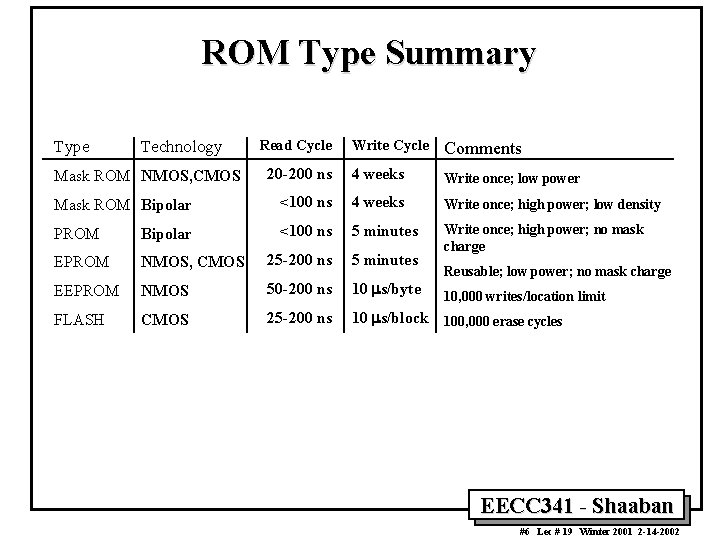
ROM Type Summary Write Cycle Comments 20 -200 ns 4 weeks Write once; low power Mask ROM Bipolar <100 ns 4 weeks Write once; high power; low density PROM Bipolar <100 ns 5 minutes EPROM NMOS, CMOS 25 -200 ns 5 minutes Write once; high power; no mask charge EEPROM NMOS 50 -200 ns 10 ms/byte FLASH CMOS 25 -200 ns 10 ms/block 100, 000 erase cycles Type Technology Mask ROM NMOS, CMOS Read Cycle Reusable; low power; no mask charge 10, 000 writes/location limit EECC 341 - Shaaban #6 Lec # 19 Winter 2001 2 -14 -2002

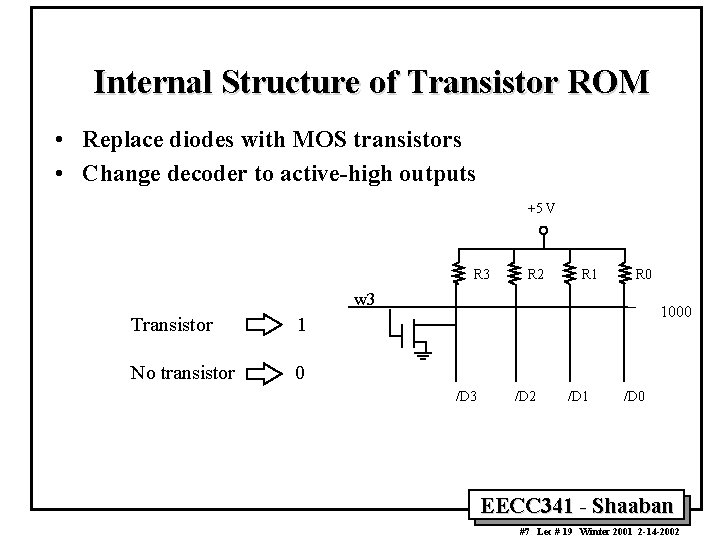
Internal Structure of Transistor ROM • Replace diodes with MOS transistors • Change decoder to active-high outputs +5 V R 3 R 2 R 1 R 0 w 3 Transistor 1 No transistor 0 1000 /D 3 /D 2 /D 1 /D 0 EECC 341 - Shaaban #7 Lec # 19 Winter 2001 2 -14 -2002

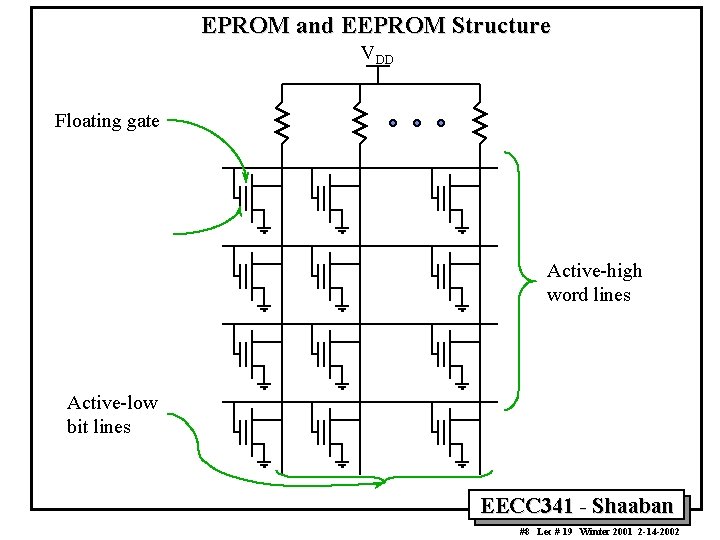
EPROM and EEPROM Structure VDD Floating gate Active-high word lines Active-low bit lines EECC 341 - Shaaban #8 Lec # 19 Winter 2001 2 -14 -2002

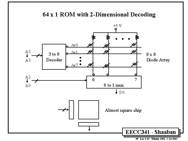
64 x 1 ROM with 2 -Dimensional Decoding +5 V · · · /w 0 A 5 A 3 A 2 A 0 3 to 8 Decoder /w 1 8 x 8 Diode Array · · /w 7 · 0 7 8 to 1 mux D 0 Almost square chip EECC 341 - Shaaban #9 Lec # 19 Winter 2001 2 -14 -2002

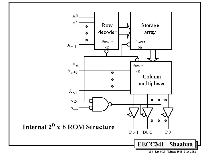
A 0 A 1 Am-1 Row decoder Power on Am Am+1 Storage array Power on Column multiplexer An-1 /CS /OE Internal 2 n x b ROM Structure Db-1 Db-2 D 0 EECC 341 - Shaaban #10 Lec # 19 Winter 2001 2 -14 -2002

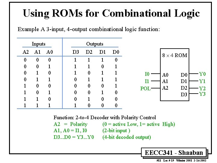
Using ROMs for Combinational Logic Example A 3 -input, 4 -output combinational logic function: Inputs A 2 A 1 A 0 0 0 1 1 1 0 0 1 1 1 D 3 1 1 1 0 0 1 Outputs D 2 D 1 1 0 0 1 1 1 0 0 0 D 0 0 1 1 0 0 0 8 ´ 4 ROM I 0 I 1 POL A 0 A 1 A 2 D 0 D 1 D 2 D 3 Y 0 Y 1 Y 2 Y 3 Function: 2 -to-4 Decoder with Polarity Control A 2 = Polarity (0 = active Low, 1= active High) A 1, A 0 = I 1, I 0 (2 -bit input ) D 3. . . D 0 = Y 3. . . Y 0 (4 -bit decoded output) EECC 341 - Shaaban #11 Lec # 19 Winter 2001 2 -14 -2002

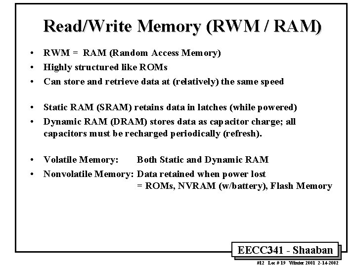
Read/Write Memory (RWM / RAM) • RWM = RAM (Random Access Memory) • Highly structured like ROMs • Can store and retrieve data at (relatively) the same speed • Static RAM (SRAM) retains data in latches (while powered) • Dynamic RAM (DRAM) stores data as capacitor charge; all capacitors must be recharged periodically (refresh). • Volatile Memory: Both Static and Dynamic RAM • Nonvolatile Memory: Data retained when power lost = ROMs, NVRAM (w/battery), Flash Memory EECC 341 - Shaaban #12 Lec # 19 Winter 2001 2 -14 -2002

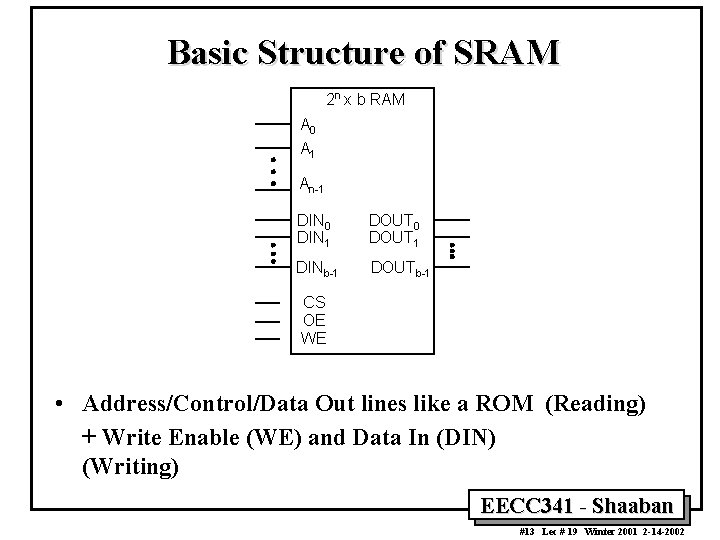
Basic Structure of SRAM 2 n x b RAM A 0 A 1 An-1 DIN 0 DIN 1 DOUT 0 DOUT 1 DINb-1 DOUTb-1 CS OE WE • Address/Control/Data Out lines like a ROM (Reading) + Write Enable (WE) and Data In (DIN) (Writing) EECC 341 - Shaaban #13 Lec # 19 Winter 2001 2 -14 -2002

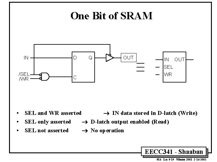
One Bit of SRAM IN D /SEL /WR C Q OUT IN OUT SEL WR • SEL and WR asserted ® IN data stored in D-latch (Write) • SEL only asserted ® D-latch output enabled (Read) • SEL not asserted ® No operation EECC 341 - Shaaban #14 Lec # 19 Winter 2001 2 -14 -2002

DIN 3 DIN 2 DIN 1 DIN 0 0 IN 1 8 x 4 SRAM 3 -to-8 Decoder A 2 A 1 A 0 2 1 0 4 IN WR WR WR OUT IN OUT IN SEL SEL WR WR IN OUT IN SEL SEL WR WR OUT IN OUT IN SEL SEL WR WR IN 7 OUT WR IN 6 IN SEL IN 5 OUT SEL IN 3 IN SEL IN 2 OUT SEL OUT IN SEL SEL WR WR IN OUT IN SEL SEL WR WR OUT OUT /WE /CS /OE DOUT 3 DOUT 2 EECC 341 DOUT 1 - Shaaban DOUT 1 #15 Lec # 19 Winter 2001 2 -14 -2002

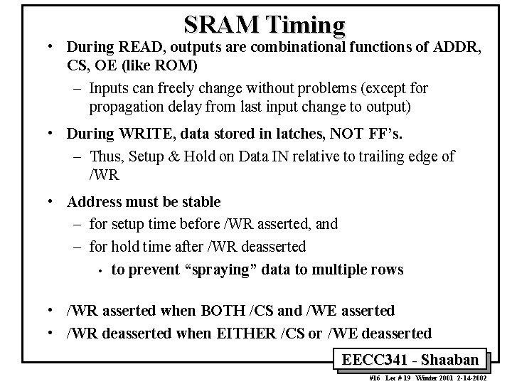
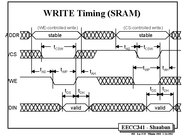
SRAM Timing • During READ, outputs are combinational functions of ADDR, CS, OE (like ROM) – Inputs can freely change without problems (except for propagation delay from last input change to output) • During WRITE, data stored in latches, NOT FF’s. – Thus, Setup & Hold on Data IN relative to trailing edge of /WR • Address must be stable – for setup time before /WR asserted, and – for hold time after /WR deasserted • to prevent “spraying” data to multiple rows • /WR asserted when BOTH /CS and /WE asserted • /WR deasserted when EITHER /CS or /WE deasserted EECC 341 - Shaaban #16 Lec # 19 Winter 2001 2 -14 -2002

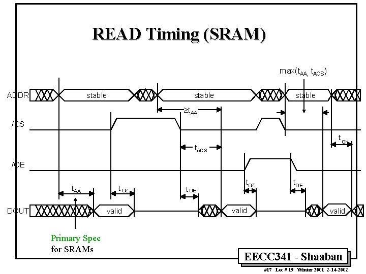
READ Timing (SRAM) max(t. AA, t. ACS) ADDR stable ³t. AA /CS t OH t. ACS /OE t. AA DOUT t OZ valid Primary Spec for SRAMs t OE t. OZ valid t. OE valid EECC 341 - Shaaban #17 Lec # 19 Winter 2001 2 -14 -2002

WRITE Timing (SRAM) (WE-controlled write) ADDR (CS-controlled write) stable t. CSW t. AS t. CSW /CS t. AS t. WP t. AH /WE t. DS DIN t. DH valid t. DS t. DH valid EECC 341 - Shaaban #18 Lec # 19 Winter 2001 2 -14 -2002

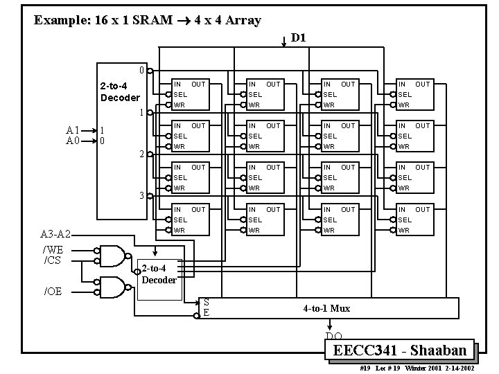
Example: 16 x 1 SRAM ® 4 x 4 Array D 1 0 IN 2 -to-4 Decoder 1 A 0 1 0 2 /OE OUT IN OUT SEL WR WR IN OUT SEL WR WR OUT IN SEL SEL WR WR IN A 3 -A 2 /WE /CS IN SEL IN 3 OUT SEL OUT IN SEL SEL WR WR OUT 2 -to-4 Decoder S E 4 -to-1 Mux DO EECC 341 - Shaaban #19 Lec # 19 Winter 2001 2 -14 -2002

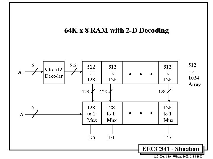
64 K x 8 RAM with 2 -D Decoding 9 A 9 to 512 Decoder 512 ´ 128 7 A 512 ´ 128 · · · 128 512 ´ 1024 Array 128 to 1 Mux D 0 D 1 · · · 128 to 1 Mux D 7 EECC 341 - Shaaban #20 Lec # 19 Winter 2001 2 -14 -2002

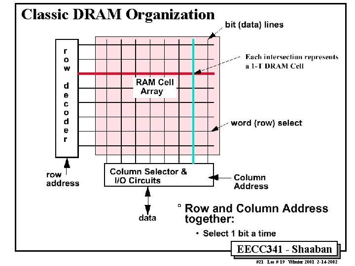
Classic DRAM Organization EECC 341 - Shaaban #21 Lec # 19 Winter 2001 2 -14 -2002

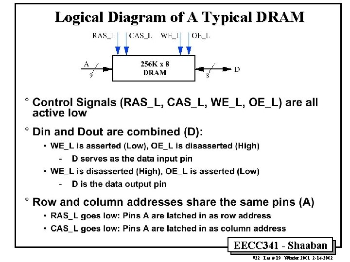
Logical Diagram of A Typical DRAM EECC 341 - Shaaban #22 Lec # 19 Winter 2001 2 -14 -2002

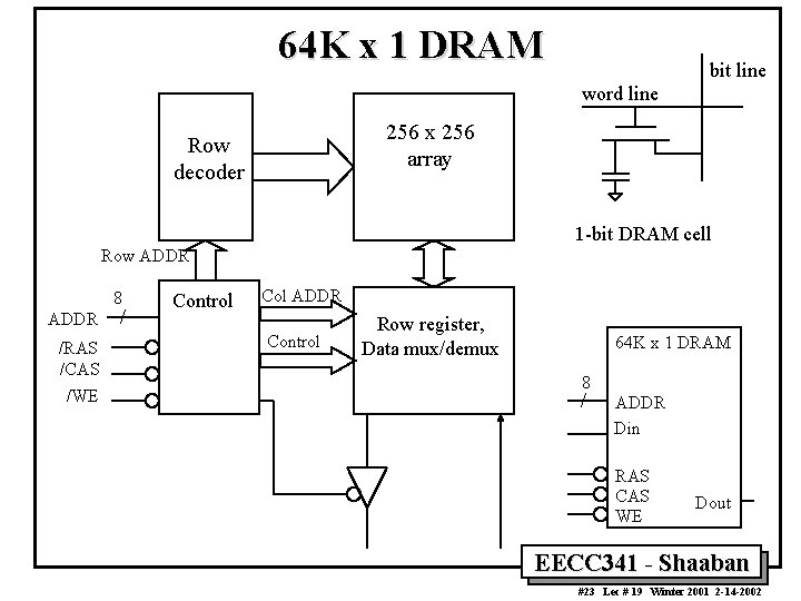
64 K x 1 DRAM bit line word line 256 x 256 array Row decoder 1 -bit DRAM cell Row ADDR 8 ADDR /RAS /CAS /WE / Control Col ADDR Control Row register, Data mux/demux 64 K x 1 DRAM 8 / ADDR Din RAS CAS WE Dout EECC 341 - Shaaban #23 Lec # 19 Winter 2001 2 -14 -2002

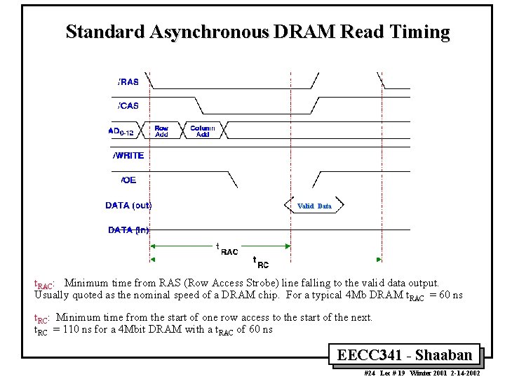
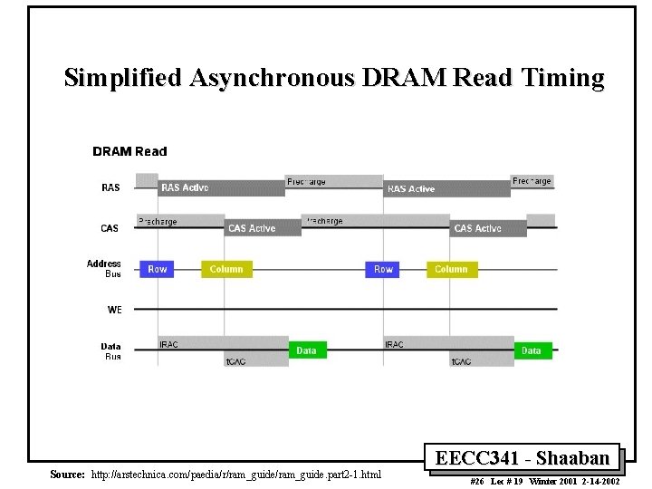
Standard Asynchronous DRAM Read Timing Valid Data t. RAC: Minimum time from RAS (Row Access Strobe) line falling to the valid data output. Usually quoted as the nominal speed of a DRAM chip. For a typical 4 Mb DRAM t. RAC = 60 ns t. RC: Minimum time from the start of one row access to the start of the next. t. RC = 110 ns for a 4 Mbit DRAM with a t. RAC of 60 ns EECC 341 - Shaaban #24 Lec # 19 Winter 2001 2 -14 -2002

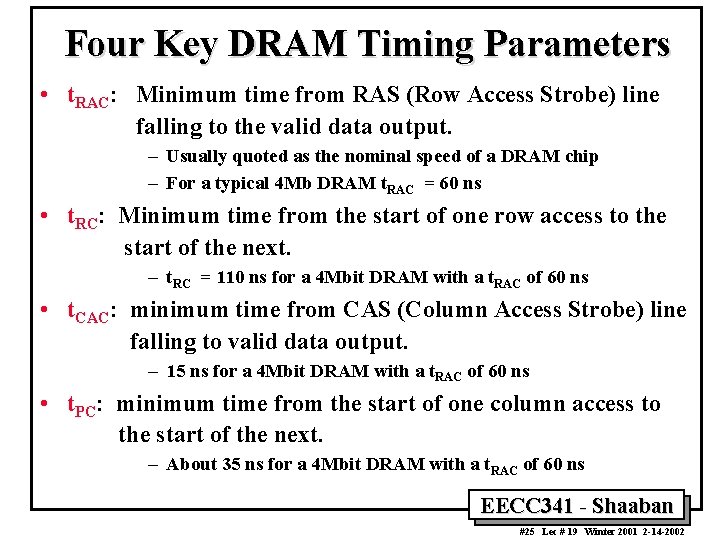
Four Key DRAM Timing Parameters • t. RAC: Minimum time from RAS (Row Access Strobe) line falling to the valid data output. – Usually quoted as the nominal speed of a DRAM chip – For a typical 4 Mb DRAM t. RAC = 60 ns • t. RC: Minimum time from the start of one row access to the start of the next. – t. RC = 110 ns for a 4 Mbit DRAM with a t. RAC of 60 ns • t. CAC: minimum time from CAS (Column Access Strobe) line falling to valid data output. – 15 ns for a 4 Mbit DRAM with a t. RAC of 60 ns • t. PC: minimum time from the start of one column access to the start of the next. – About 35 ns for a 4 Mbit DRAM with a t. RAC of 60 ns EECC 341 - Shaaban #25 Lec # 19 Winter 2001 2 -14 -2002

Simplified Asynchronous DRAM Read Timing Source: http: //arstechnica. com/paedia/r/ram_guide. part 2 -1. html EECC 341 - Shaaban #26 Lec # 19 Winter 2001 2 -14 -2002

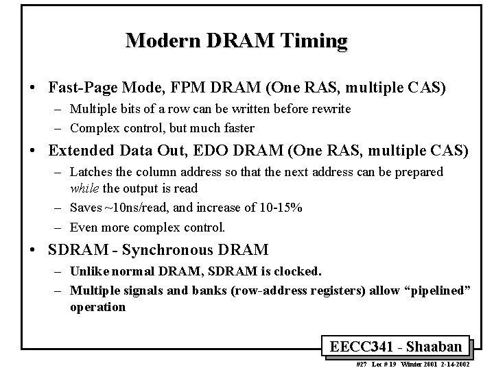
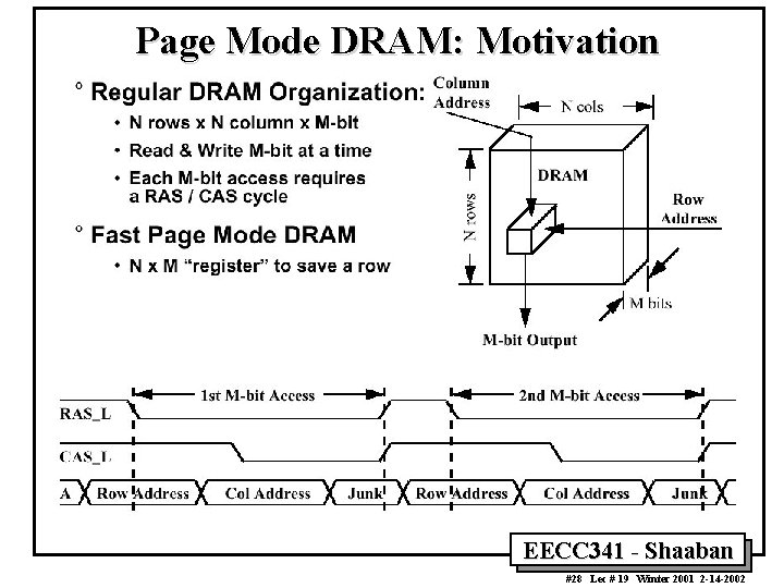
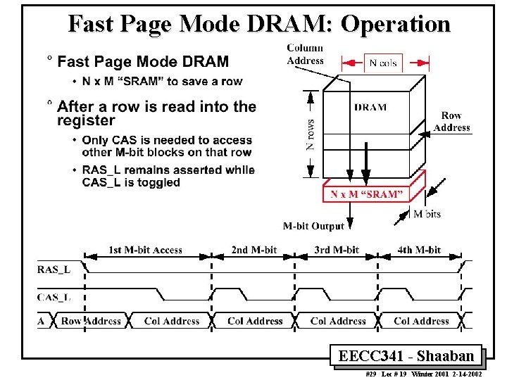
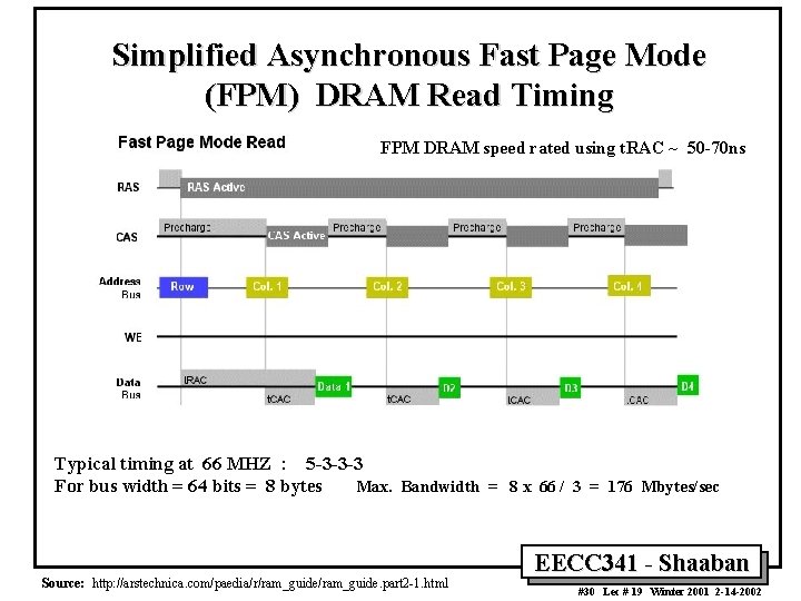
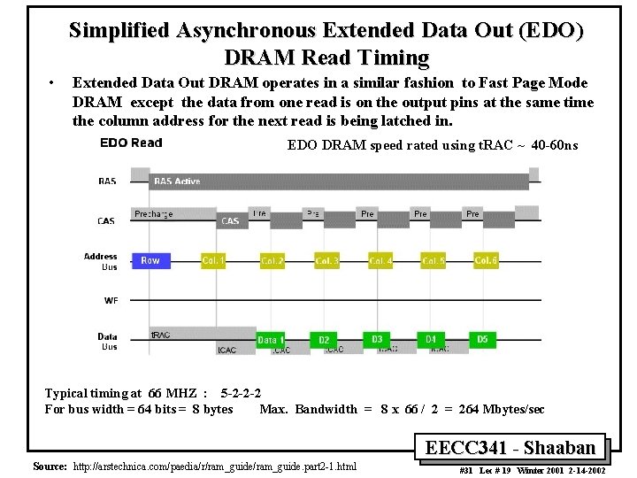
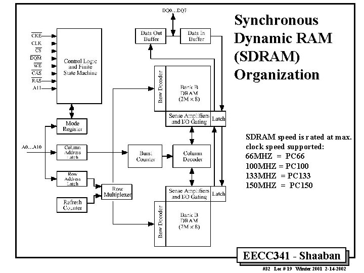
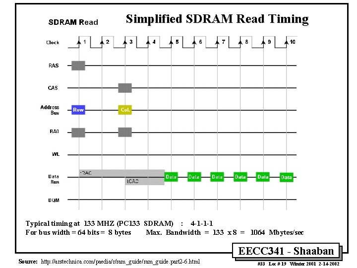
Modern DRAM Timing • Fast-Page Mode, FPM DRAM (One RAS, multiple CAS) – Multiple bits of a row can be written before rewrite – Complex control, but much faster • Extended Data Out, EDO DRAM (One RAS, multiple CAS) – Latches the column address so that the next address can be prepared while the output is read – Saves ~10 ns/read, and increase of 10 -15% – Even more complex control. • SDRAM - Synchronous DRAM – Unlike normal DRAM, SDRAM is clocked. – Multiple signals and banks (row-address registers) allow “pipelined” operation EECC 341 - Shaaban #27 Lec # 19 Winter 2001 2 -14 -2002

Page Mode DRAM: Motivation EECC 341 - Shaaban #28 Lec # 19 Winter 2001 2 -14 -2002

Fast Page Mode DRAM: Operation EECC 341 - Shaaban #29 Lec # 19 Winter 2001 2 -14 -2002

Simplified Asynchronous Fast Page Mode (FPM) DRAM Read Timing FPM DRAM speed rated using t. RAC ~ 50 -70 ns Typical timing at 66 MHZ : 5 -3 -3 -3 For bus width = 64 bits = 8 bytes Max. Bandwidth = 8 x 66 / 3 = 176 Mbytes/sec Source: http: //arstechnica. com/paedia/r/ram_guide. part 2 -1. html EECC 341 - Shaaban #30 Lec # 19 Winter 2001 2 -14 -2002

Simplified Asynchronous Extended Data Out (EDO) DRAM Read Timing • Extended Data Out DRAM operates in a similar fashion to Fast Page Mode DRAM except the data from one read is on the output pins at the same time the column address for the next read is being latched in. EDO DRAM speed rated using t. RAC ~ 40 -60 ns Typical timing at 66 MHZ : 5 -2 -2 -2 For bus width = 64 bits = 8 bytes Max. Bandwidth = 8 x 66 / 2 = 264 Mbytes/sec EECC 341 - Shaaban Source: http: //arstechnica. com/paedia/r/ram_guide. part 2 -1. html #31 Lec # 19 Winter 2001 2 -14 -2002

Synchronous Dynamic RAM (SDRAM) Organization SDRAM speed is rated at max. clock speed supported: 66 MHZ = PC 66 100 MHZ = PC 100 133 MHZ = PC 133 150 MHZ = PC 150 EECC 341 - Shaaban #32 Lec # 19 Winter 2001 2 -14 -2002

Simplified SDRAM Read Timing Typical timing at 133 MHZ (PC 133 SDRAM) : 4 -1 -1 -1 For bus width = 64 bits = 8 bytes Max. Bandwidth = 133 x 8 = 1064 Mbytes/sec EECC 341 - Shaaban Source: http: //arstechnica. com/paedia/r/ram_guide. part 2 -6. html #33 Lec # 19 Winter 2001 2 -14 -2002

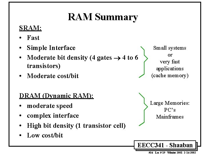
RAM Summary SRAM: • Fast • Simple Interface • Moderate bit density (4 gates ® 4 to 6 transistors) • Moderate cost/bit DRAM (Dynamic RAM): • moderate speed • complex interface • High bit density (1 transistor cell) • Low cost/bit Small systems or very fast applications (cache memory) Large Memories: PC’s Mainframes EECC 341 - Shaaban #34 Lec # 19 Winter 2001 2 -14 -2002