Topic 2 Vector Processing Vector Architectures Lasciate Ogne


![Vector Length Control An Example: for(i = 0; i < n; ++i) y[i] = Vector Length Control An Example: for(i = 0; i < n; ++i) y[i] =](https://slidetodoc.com/presentation_image_h2/45c4aaef8629856a2eddf10d98caa3cb/image-12.jpg)

![Gather Operation V 0 V 1[i] = A[V 0[i]] VL 4 A 0 100 Gather Operation V 0 V 1[i] = A[V 0[i]] VL 4 A 0 100](https://slidetodoc.com/presentation_image_h2/45c4aaef8629856a2eddf10d98caa3cb/image-44.jpg)
![Scatter Operation A[V 0[i]] = V 1[i] VL 4 A 0 100 Example: A[V Scatter Operation A[V 0[i]] = V 1[i] VL 4 A 0 100 Example: A[V](https://slidetodoc.com/presentation_image_h2/45c4aaef8629856a2eddf10d98caa3cb/image-45.jpg)




![Another Memory Layout Modulo 0 A[0] B[6] W[4] Modulo 1 A[1] B[7] W[5] Modulo Another Memory Layout Modulo 0 A[0] B[6] W[4] Modulo 1 A[1] B[7] W[5] Modulo](https://slidetodoc.com/presentation_image_h2/45c4aaef8629856a2eddf10d98caa3cb/image-73.jpg)



- Slides: 88

Topic 2 Vector Processing & Vector Architectures Lasciate Ogne Speranza, Voi Ch’Intrate Dante’s Inferno 9/18/2006 ELEG 652 -06 F 1

Reading List • Slides: Topic 2 x • Henn&Patt: Appendix G • Other assigned readings from homework and classes 9/18/2006 ELEG 652 -06 F 2

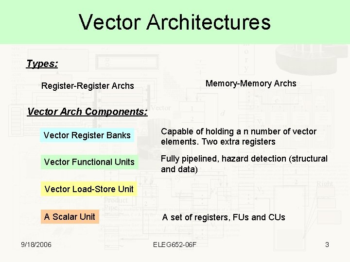
Vector Architectures Types: Memory-Memory Archs Register-Register Archs Vector Arch Components: Vector Register Banks Capable of holding a n number of vector elements. Two extra registers Vector Functional Units Fully pipelined, hazard detection (structural and data) Vector Load-Store Unit A Scalar Unit 9/18/2006 A set of registers, FUs and CUs ELEG 652 -06 F 3

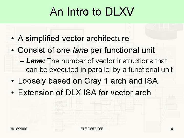
An Intro to DLXV • A simplified vector architecture • Consist of one lane per functional unit – Lane: The number of vector instructions that can be executed in parallel by a functional unit • Loosely based on Cray 1 arch and ISA • Extension of DLX ISA for vector arch 9/18/2006 ELEG 652 -06 F 4

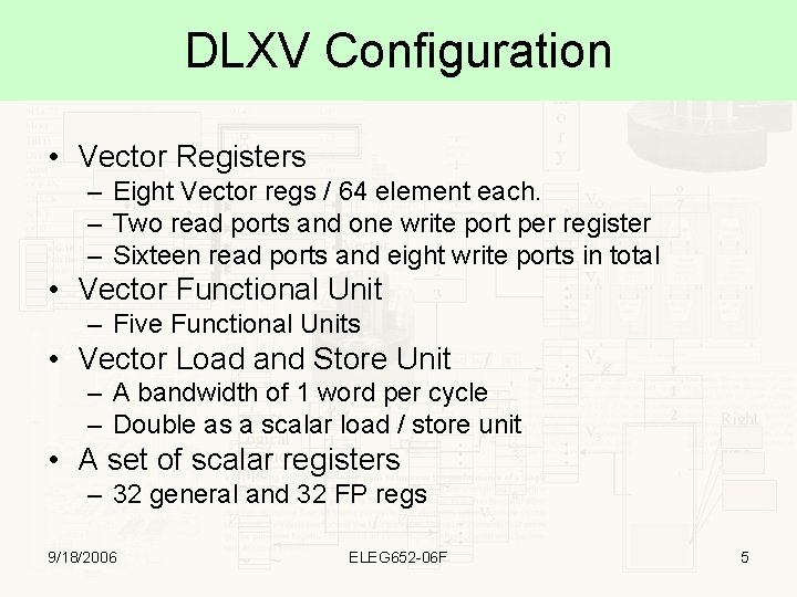
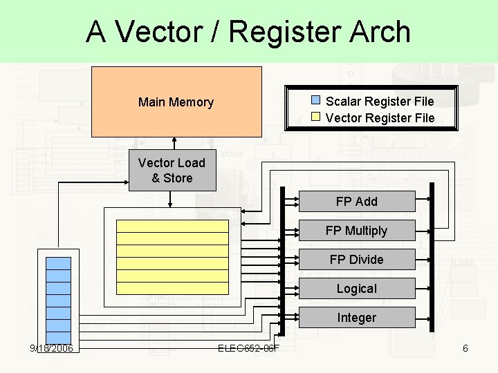
DLXV Configuration • Vector Registers – Eight Vector regs / 64 element each. – Two read ports and one write port per register – Sixteen read ports and eight write ports in total • Vector Functional Unit – Five Functional Units • Vector Load and Store Unit – A bandwidth of 1 word per cycle – Double as a scalar load / store unit • A set of scalar registers – 32 general and 32 FP regs 9/18/2006 ELEG 652 -06 F 5

A Vector / Register Arch Scalar Register File Vector Register File Main Memory Vector Load & Store FP Add FP Multiply FP Divide Logical Integer 9/18/2006 ELEG 652 -06 F 6

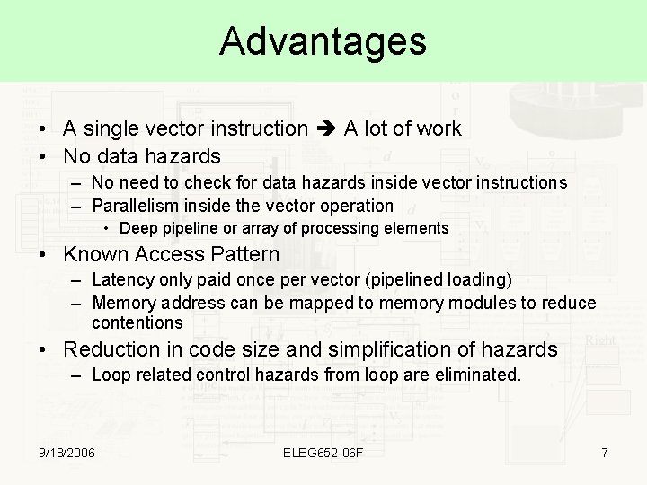
Advantages • A single vector instruction A lot of work • No data hazards – No need to check for data hazards inside vector instructions – Parallelism inside the vector operation • Deep pipeline or array of processing elements • Known Access Pattern – Latency only paid once per vector (pipelined loading) – Memory address can be mapped to memory modules to reduce contentions • Reduction in code size and simplification of hazards – Loop related control hazards from loop are eliminated. 9/18/2006 ELEG 652 -06 F 7

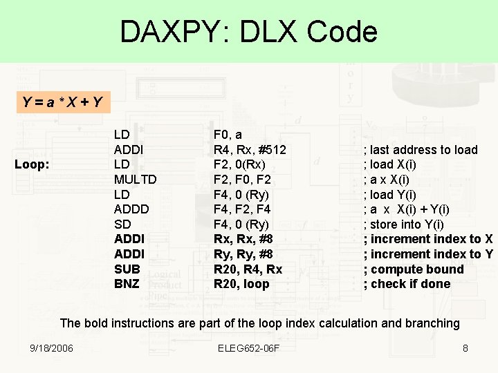
DAXPY: DLX Code Y=a*X+Y LD ADDI LD MULTD LD ADDD SD ADDI SUB BNZ Loop: F 0, a R 4, Rx, #512 F 2, 0(Rx) F 2, F 0, F 2 F 4, 0 (Ry) F 4, F 2, F 4, 0 (Ry) Rx, #8 Ry, #8 R 20, R 4, Rx R 20, loop ; last address to load ; load X(i) ; a x X(i) ; load Y(i) ; a x X(i) + Y(i) ; store into Y(i) ; increment index to X ; increment index to Y ; compute bound ; check if done The bold instructions are part of the loop index calculation and branching 9/18/2006 ELEG 652 -06 F 8

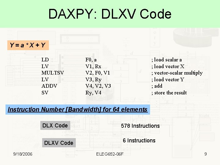
DAXPY: DLXV Code Y=a*X+Y LD LV MULTSV LV ADDV SV F 0, a V 1, Rx V 2, F 0, V 1 V 3, Ry V 4, V 2, V 3 Ry, V 4 ; load scalar a ; load vector X ; vector-scalar multiply ; load vector Y ; add ; store the result Instruction Number [Bandwidth] for 64 elements DLX Code DLXV Code 9/18/2006 578 Instructions 6 Instructions ELEG 652 -06 F 9

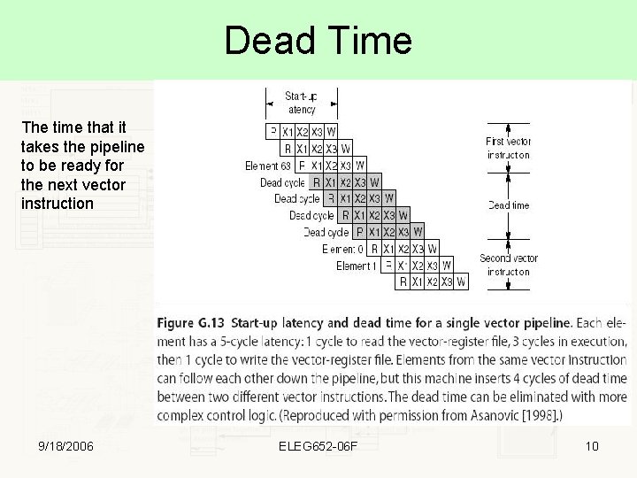
Dead Time The time that it takes the pipeline to be ready for the next vector instruction 9/18/2006 ELEG 652 -06 F 10

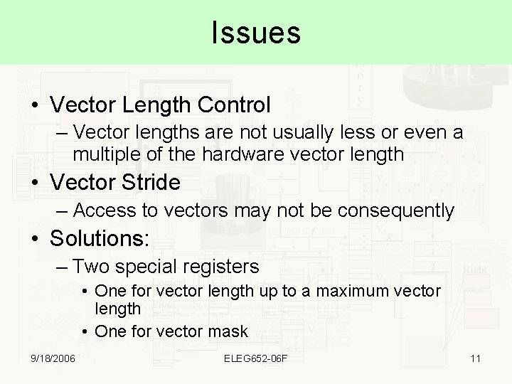
Issues • Vector Length Control – Vector lengths are not usually less or even a multiple of the hardware vector length • Vector Stride – Access to vectors may not be consequently • Solutions: – Two special registers • One for vector length up to a maximum vector length • One for vector mask 9/18/2006 ELEG 652 -06 F 11
![Vector Length Control An Example fori 0 i n i yi Vector Length Control An Example: for(i = 0; i < n; ++i) y[i] =](https://slidetodoc.com/presentation_image_h2/45c4aaef8629856a2eddf10d98caa3cb/image-12.jpg)
Vector Length Control An Example: for(i = 0; i < n; ++i) y[i] = a * x[i] +y[i] Question: Assume the maximum hardware vector length is MVL which may be less than n. How should we do the above computation ? 9/18/2006 ELEG 652 -06 F 12

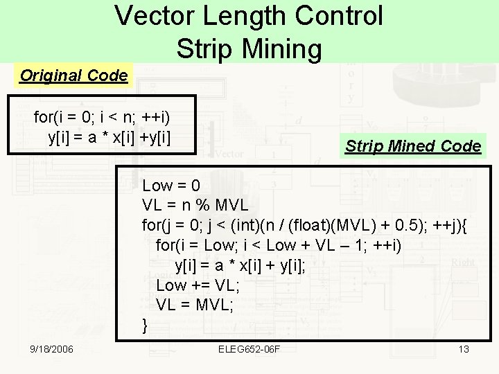
Vector Length Control Strip Mining Original Code for(i = 0; i < n; ++i) y[i] = a * x[i] +y[i] Strip Mined Code Low = 0 VL = n % MVL for(j = 0; j < (int)(n / (float)(MVL) + 0. 5); ++j){ for(i = Low; i < Low + VL – 1; ++i) y[i] = a * x[i] + y[i]; Low += VL; VL = MVL; } 9/18/2006 ELEG 652 -06 F 13

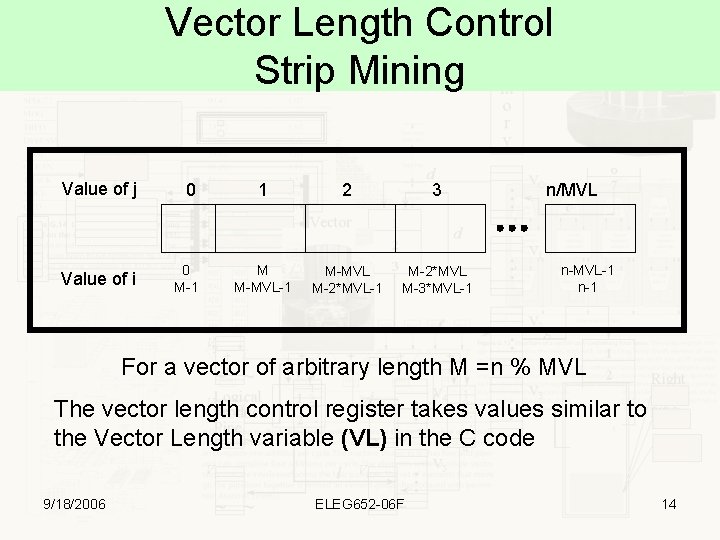
Vector Length Control Strip Mining Value of j 0 Value of i 0 M-1 1 2 3 M M-MVL-1 M-MVL M-2*MVL-1 M-2*MVL M-3*MVL-1 n/MVL n-MVL-1 n-1 For a vector of arbitrary length M =n % MVL The vector length control register takes values similar to the Vector Length variable (VL) in the C code 9/18/2006 ELEG 652 -06 F 14

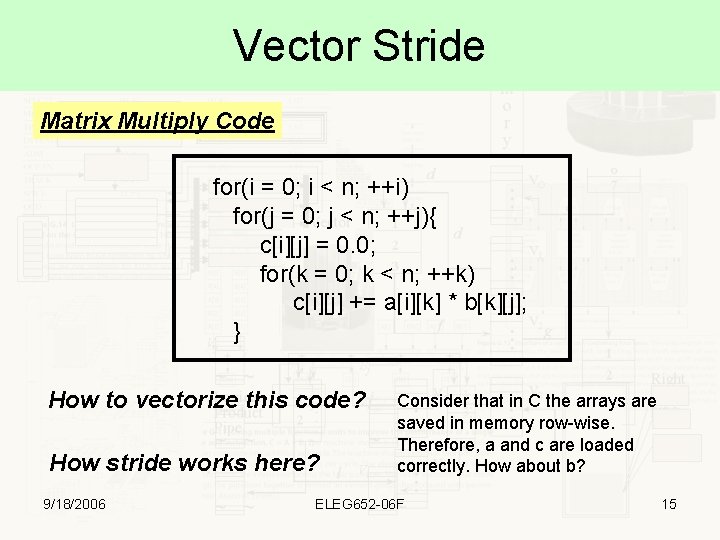
Vector Stride Matrix Multiply Code for(i = 0; i < n; ++i) for(j = 0; j < n; ++j){ c[i][j] = 0. 0; for(k = 0; k < n; ++k) c[i][j] += a[i][k] * b[k][j]; } How to vectorize this code? How stride works here? 9/18/2006 Consider that in C the arrays are saved in memory row-wise. Therefore, a and c are loaded correctly. How about b? ELEG 652 -06 F 15

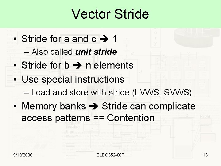
Vector Stride • Stride for a and c 1 – Also called unit stride • Stride for b n elements • Use special instructions – Load and store with stride (LVWS, SVWS) • Memory banks Stride can complicate access patterns == Contention 9/18/2006 ELEG 652 -06 F 16

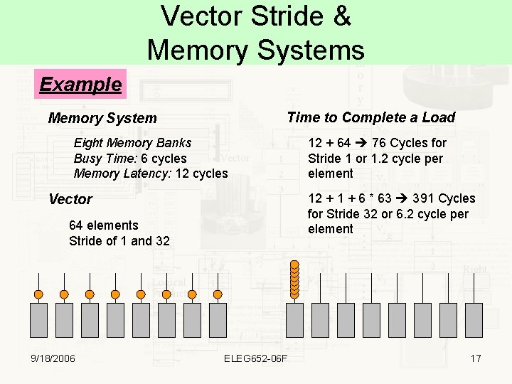
Vector Stride & Memory Systems Example Time to Complete a Load Memory System Eight Memory Banks Busy Time: 6 cycles Memory Latency: 12 cycles 12 + 1 + 6 * 63 391 Cycles for Stride 32 or 6. 2 cycle per element Vector 64 elements Stride of 1 and 32 9/18/2006 12 + 64 76 Cycles for Stride 1 or 1. 2 cycle per element ELEG 652 -06 F 17

Cray-1 “The World Most Expensive Love Seat. . . ” Picture courtesy of Cray Original Source: Cray 1 Computer System Hardware Reference Manual 9/18/2006 ELEG 652 -06 F 18

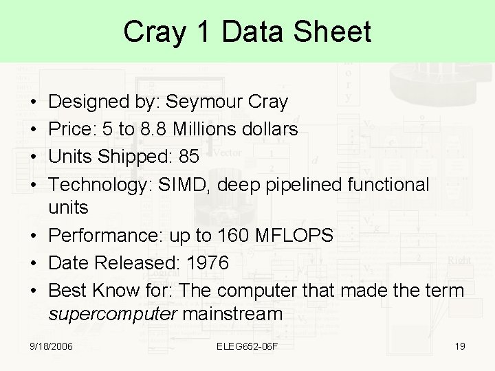
Cray 1 Data Sheet • • Designed by: Seymour Cray Price: 5 to 8. 8 Millions dollars Units Shipped: 85 Technology: SIMD, deep pipelined functional units • Performance: up to 160 MFLOPS • Date Released: 1976 • Best Know for: The computer that made the term supercomputer mainstream 9/18/2006 ELEG 652 -06 F 19

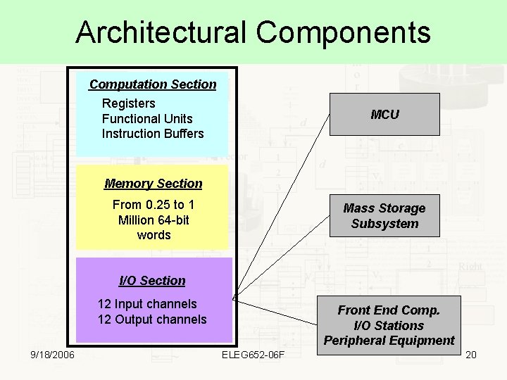
Architectural Components Computation Section Registers Functional Units Instruction Buffers MCU Memory Section From 0. 25 to 1 Million 64 -bit words Mass Storage Subsystem I/O Section 12 Input channels 12 Output channels 9/18/2006 Front End Comp. I/O Stations Peripheral Equipment ELEG 652 -06 F 20

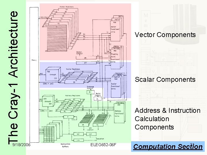
The Cray-1 Architecture 9/18/2006 Vector Components Scalar Components Address & Instruction Calculation Components ELEG 652 -06 F 21 Computation Section

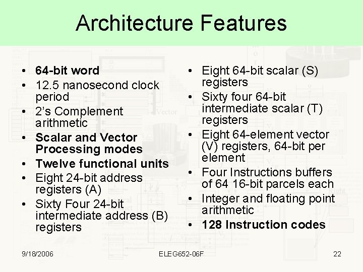
Architecture Features • 64 -bit word • 12. 5 nanosecond clock period • 2’s Complement arithmetic • Scalar and Vector Processing modes • Twelve functional units • Eight 24 -bit address registers (A) • Sixty Four 24 -bit intermediate address (B) registers 9/18/2006 • Eight 64 -bit scalar (S) registers • Sixty four 64 -bit intermediate scalar (T) registers • Eight 64 -element vector (V) registers, 64 -bit per element • Four Instructions buffers of 64 16 -bit parcels each • Integer and floating point arithmetic • 128 Instruction codes ELEG 652 -06 F 22

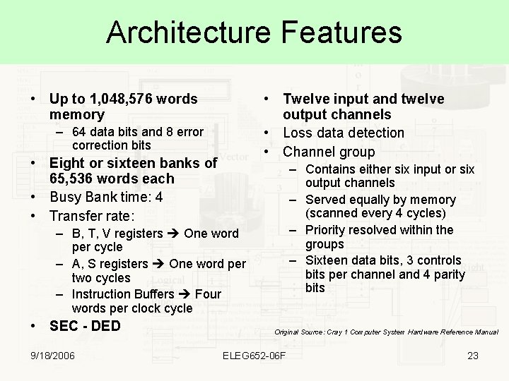
Architecture Features • Up to 1, 048, 576 words memory • Twelve input and twelve output channels • Loss data detection • Channel group – 64 data bits and 8 error correction bits • Eight or sixteen banks of 65, 536 words each • Busy Bank time: 4 • Transfer rate: – Contains either six input or six output channels – Served equally by memory (scanned every 4 cycles) – Priority resolved within the groups – Sixteen data bits, 3 controls bits per channel and 4 parity bits – B, T, V registers One word per cycle – A, S registers One word per two cycles – Instruction Buffers Four words per clock cycle • SEC - DED 9/18/2006 Original Source: Cray 1 Computer System Hardware Reference Manual ELEG 652 -06 F 23

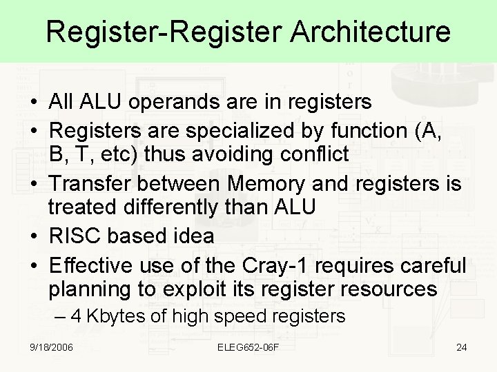
Register-Register Architecture • All ALU operands are in registers • Registers are specialized by function (A, B, T, etc) thus avoiding conflict • Transfer between Memory and registers is treated differently than ALU • RISC based idea • Effective use of the Cray-1 requires careful planning to exploit its register resources – 4 Kbytes of high speed registers 9/18/2006 ELEG 652 -06 F 24

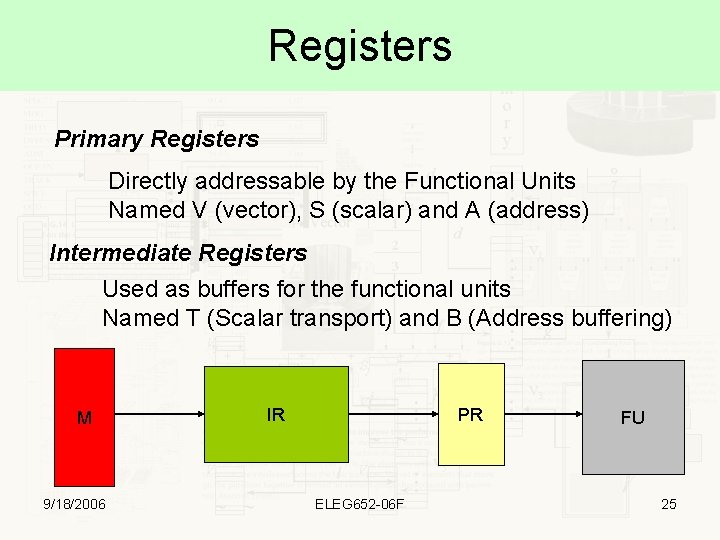
Registers Primary Registers Directly addressable by the Functional Units Named V (vector), S (scalar) and A (address) Intermediate Registers Used as buffers for the functional units Named T (Scalar transport) and B (Address buffering) M 9/18/2006 IR PR ELEG 652 -06 F FU 25

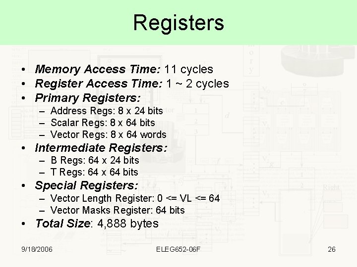
Registers • Memory Access Time: 11 cycles • Register Access Time: 1 ~ 2 cycles • Primary Registers: – Address Regs: 8 x 24 bits – Scalar Regs: 8 x 64 bits – Vector Regs: 8 x 64 words • Intermediate Registers: – B Regs: 64 x 24 bits – T Regs: 64 x 64 bits • Special Registers: – Vector Length Register: 0 <= VL <= 64 – Vector Masks Register: 64 bits • Total Size: 4, 888 bytes 9/18/2006 ELEG 652 -06 F 26

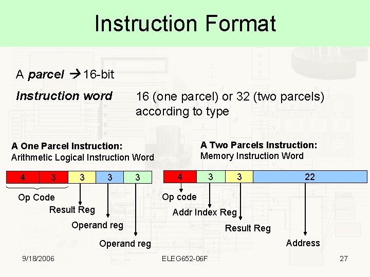
Instruction Format A parcel 16 -bit Instruction word 16 (one parcel) or 32 (two parcels) according to type A Two Parcels Instruction: Memory Instruction Word A One Parcel Instruction: Arithmetic Logical Instruction Word 4 3 3 4 3 22 Op code Op Code Result Reg Addr Index Reg Operand reg Result Reg Address Operand reg 9/18/2006 3 ELEG 652 -06 F 27

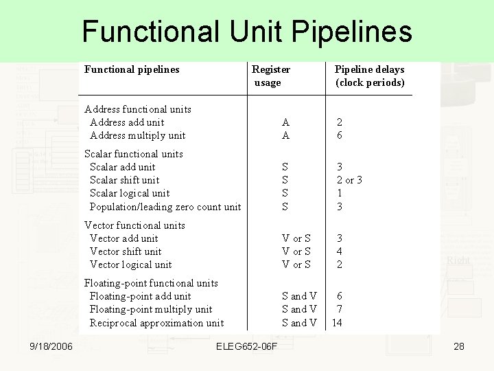
Functional Unit Pipelines Functional pipelines 9/18/2006 Register usage Pipeline delays (clock periods) Address functional units Address add unit Address multiply unit A A 2 6 Scalar functional units Scalar add unit Scalar shift unit Scalar logical unit Population/leading zero count unit S S 3 2 or 3 1 3 Vector functional units Vector add unit Vector shift unit Vector logical unit V or S 3 4 2 Floating-point functional units Floating-point add unit Floating-point multiply unit Reciprocal approximation unit S and V ELEG 652 -06 F 6 7 14 28

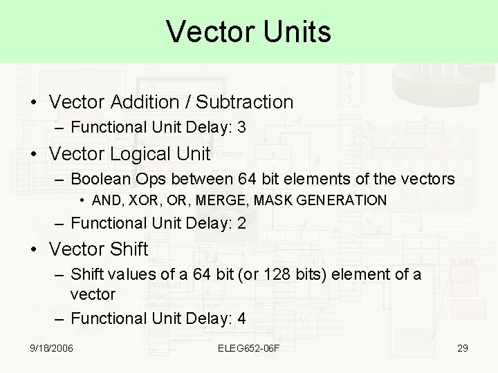
Vector Units • Vector Addition / Subtraction – Functional Unit Delay: 3 • Vector Logical Unit – Boolean Ops between 64 bit elements of the vectors • AND, XOR, MERGE, MASK GENERATION – Functional Unit Delay: 2 • Vector Shift – Shift values of a 64 bit (or 128 bits) element of a vector – Functional Unit Delay: 4 9/18/2006 ELEG 652 -06 F 29

Instruction Set • • 128 Instructions Ten Vector Types Thirteen Scalar Types Three Addressing Modes 9/18/2006 ELEG 652 -06 F 30

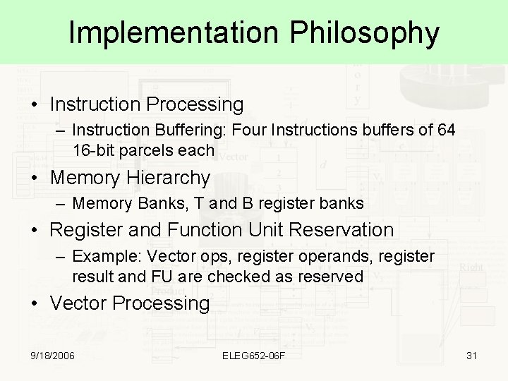
Implementation Philosophy • Instruction Processing – Instruction Buffering: Four Instructions buffers of 64 16 -bit parcels each • Memory Hierarchy – Memory Banks, T and B register banks • Register and Function Unit Reservation – Example: Vector ops, register operands, register result and FU are checked as reserved • Vector Processing 9/18/2006 ELEG 652 -06 F 31

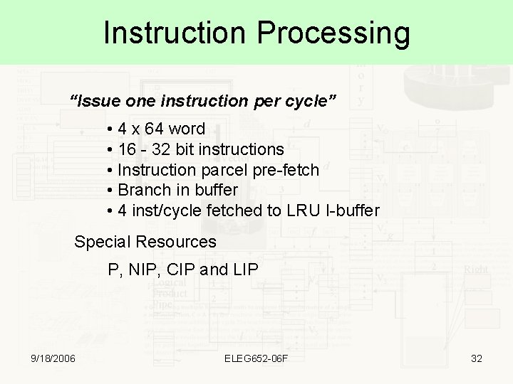
Instruction Processing “Issue one instruction per cycle” • 4 x 64 word • 16 - 32 bit instructions • Instruction parcel pre-fetch • Branch in buffer • 4 inst/cycle fetched to LRU I-buffer Special Resources P, NIP, CIP and LIP 9/18/2006 ELEG 652 -06 F 32

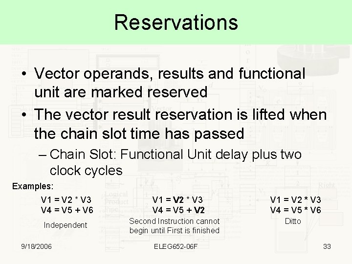
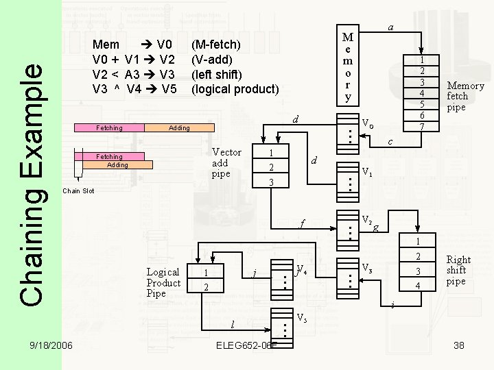
Reservations • Vector operands, results and functional unit are marked reserved • The vector result reservation is lifted when the chain slot time has passed – Chain Slot: Functional Unit delay plus two clock cycles Examples: V 1 = V 2 * V 3 V 4 = V 5 + V 6 Independent 9/18/2006 V 1 = V 2 * V 3 V 4 = V 5 + V 2 Second Instruction cannot begin until First is finished ELEG 652 -06 F V 1 = V 2 * V 3 V 4 = V 5 * V 6 Ditto 33

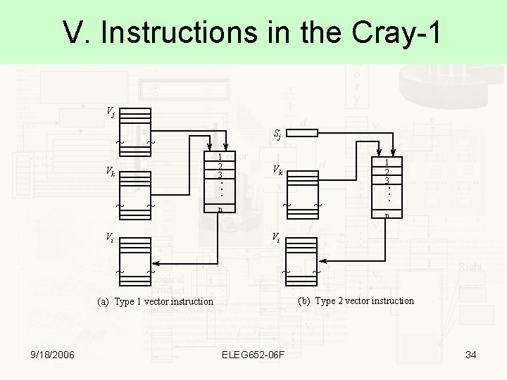
V. Instructions in the Cray-1 Vj ~ 1 2 3 ~ ~ Vi 1 2 3 Vk . . . Vk n ~ ~ n Vi ~ ~ (b) Type 2 vector instruction (a) Type 1 vector instruction 9/18/2006 . . . ~ Sj ELEG 652 -06 F 34

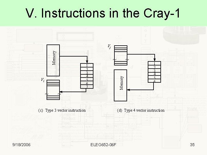
V. Instructions in the Cray-1 Memory Vj ~ Vi ~ Memory 1 2 3 4 5 6 7 1 2 3 4 5 6 ~ (c) Type 3 vector instruction 9/18/2006 ~ (d) Type 4 vector instruction ELEG 652 -06 F 35

Vector Loops • Long vectors with N > 64 are sectioned • Each time through a vector loop 64 elements are processed • Remainder handling • “transparent” to the programmer 9/18/2006 ELEG 652 -06 F 36

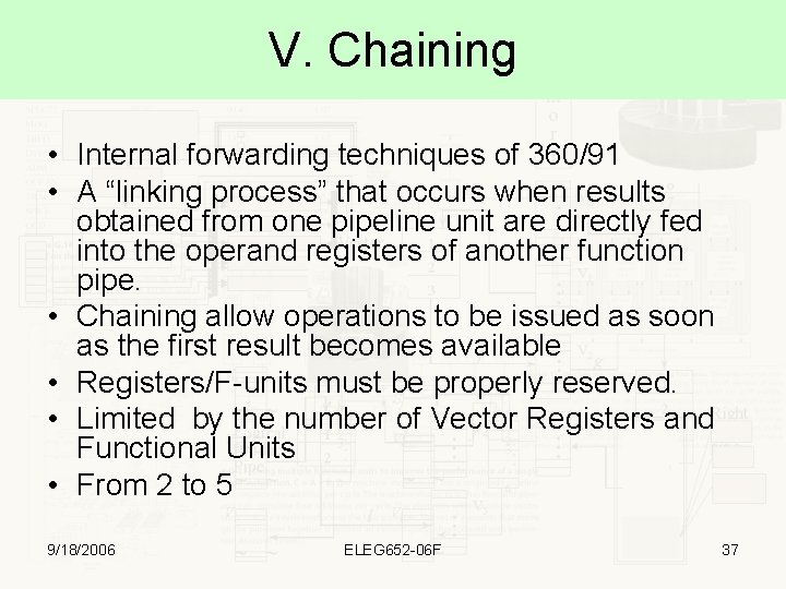
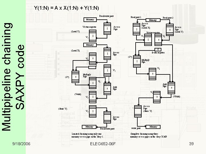
V. Chaining • Internal forwarding techniques of 360/91 • A “linking process” that occurs when results obtained from one pipeline unit are directly fed into the operand registers of another function pipe. • Chaining allow operations to be issued as soon as the first result becomes available • Registers/F-units must be properly reserved. • Limited by the number of Vector Registers and Functional Units • From 2 to 5 9/18/2006 ELEG 652 -06 F 37

d . . . Adding 1 f VO j 1 2 j. V 4 . . . Logical Product Pipe Memory fetch pipe c V 1 V 2 g 1 2 V 3 3 4 Right shift pipe i l 9/18/2006 . . . 3 Chain Slot 1 2 3 4 5 6 7 d 2 . . . Vector add pipe Fetching Adding . . . Fetching M e m o r y (M-fetch) (V-add) (left shift) (logical product) . . . Chaining Example Mem V 0 + V 1 V 2 < A 3 V 3 ^ V 4 V 5 a ELEG 652 -06 F V 5 38

Y(1: N) = A x X(1: N) + Y(1: N) Read/write port Read port 1 Access Pipe (Load X) . . . (Load Y) Access Pipe (Load Y) V 2 . . . V 1 . . Vector register V 1 Memory S Scalar register (S*) . . Multiply Pipe . . Add Pipe V 3. . Multiply Pipe . . (S*) V 1 . . S V 3 Add Pipe V 4 . . (Vadd) (VAdd) Access Pipe (Store Y) Access Pipe. . (Store Y) . . V 2 Access Pipe . . (Load X) Memory Read/write port Limited chaining using only one memory-access pipe in the Gray 1 9/18/2006 Read port 2 Memory Vector register . . Multipipeline chaining SAXPY code Memory ELEG 652 -06 F write port Memory Complete chaining using three memory-access pipes in the Cray X-MP 39

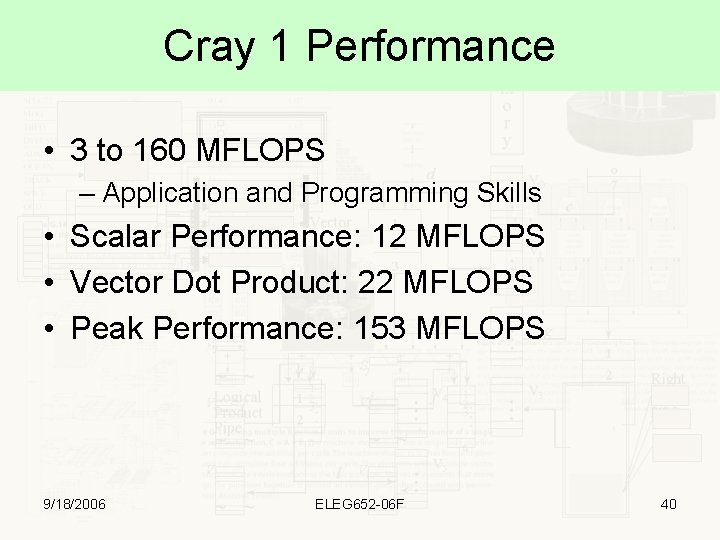
Cray 1 Performance • 3 to 160 MFLOPS – Application and Programming Skills • Scalar Performance: 12 MFLOPS • Vector Dot Product: 22 MFLOPS • Peak Performance: 153 MFLOPS 9/18/2006 ELEG 652 -06 F 40

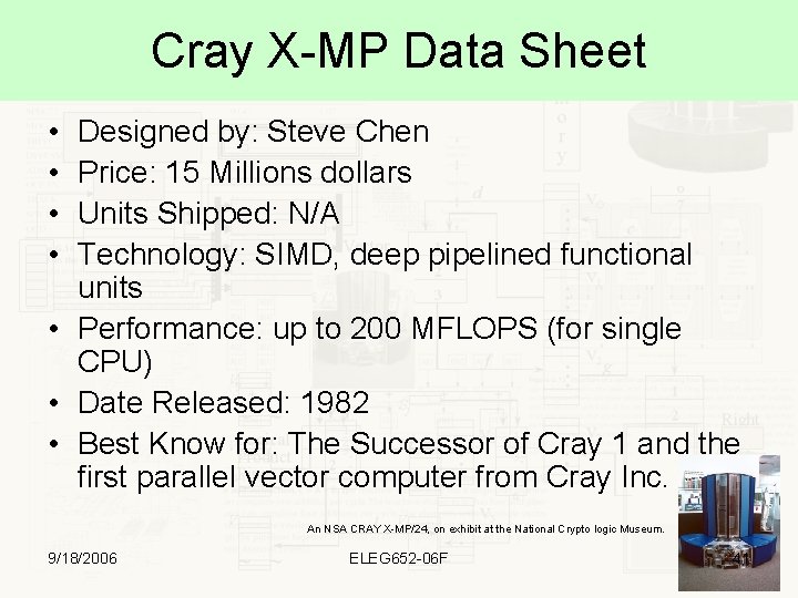
Cray X-MP Data Sheet • • Designed by: Steve Chen Price: 15 Millions dollars Units Shipped: N/A Technology: SIMD, deep pipelined functional units • Performance: up to 200 MFLOPS (for single CPU) • Date Released: 1982 • Best Know for: The Successor of Cray 1 and the first parallel vector computer from Cray Inc. An NSA CRAY X-MP/24, on exhibit at the National Crypto logic Museum. 9/18/2006 ELEG 652 -06 F 41

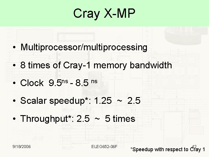
Cray X-MP • Multiprocessor/multiprocessing • 8 times of Cray-1 memory bandwidth • Clock 9. 5 ns - 8. 5 ns • Scalar speedup*: 1. 25 ~ 2. 5 • Throughput*: 2. 5 ~ 5 times 9/18/2006 ELEG 652 -06 F 42 *Speedup with respect to Cray 1

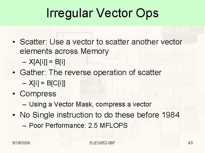
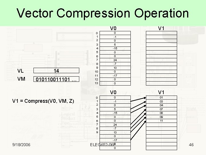
Irregular Vector Ops • Scatter: Use a vector to scatter another vector elements across Memory – X[A[i]] = B[i] • Gather: The reverse operation of scatter – X[i] = B[C[i]] • Compress – Using a Vector Mask, compress a vector • No Single instruction to do these before 1984 – Poor Performance: 2. 5 MFLOPS 9/18/2006 ELEG 652 -06 F 43
![Gather Operation V 0 V 1i AV 0i VL 4 A 0 100 Gather Operation V 0 V 1[i] = A[V 0[i]] VL 4 A 0 100](https://slidetodoc.com/presentation_image_h2/45c4aaef8629856a2eddf10d98caa3cb/image-44.jpg)
Gather Operation V 0 V 1[i] = A[V 0[i]] VL 4 A 0 100 Example: V 1[2] = A[V 0[2]] = A[7] = 250 9/18/2006 V 1 4 2 7 0 200 300 400 500 600 700 100 250 350 V 1 4 2 7 0 600 400 250 200 ELEG 652 -06 F Memory Contents / Addresses 100 140 180 1 C 0 200 240 280 2 C 0 300 Memory Contents / Addresses 200 300 400 500 600 700 100 250 350 100 140 180 1 C 0 200 240 280 2 C 0 30044 0 1 2 3 4 5 6 7 8
![Scatter Operation AV 0i V 1i VL 4 A 0 100 Example AV Scatter Operation A[V 0[i]] = V 1[i] VL 4 A 0 100 Example: A[V](https://slidetodoc.com/presentation_image_h2/45c4aaef8629856a2eddf10d98caa3cb/image-45.jpg)
Scatter Operation A[V 0[i]] = V 1[i] VL 4 A 0 100 Example: A[V 0[0]] = V 1[0] A[4] = 200 *(0 x 200)= 200 9/18/2006 V 0 V 1 4 2 7 0 200 300 400 500 ELEG 652 -06 F Memory Contents / Addresses x x x x x 100 140 180 1 C 0 200 240 280 2 C 0 300 Memory Contents / Addresses 500 x 300 x 200 x x 400 x 100 140 180 1 C 0 200 240 280 2 C 0 30045 0 1 2 3 4 5 6 7 8

Vector Compression Operation V 0 0 1 2 VL 14 VM 010110011101 … 3 4 5 6 7 8 9 10 11 12 13 V 0 V 1 = Compress(V 0, VM, Z) 9/18/2006 V 1 0 -1 0 5 -15 0 0 24 -7 13 0 -17 0 0 1 -1 2 0 3 5 4 -15 5 0 0 6 7 24 8 -7 9 13 0 -17 ELEG 652 -06 F 0 0 V 1 01 03 04 07 08 09 11 46

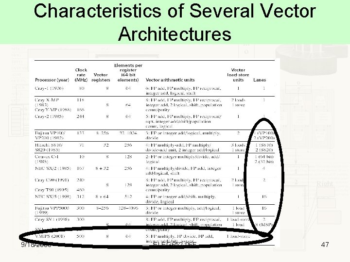
Characteristics of Several Vector Architectures 9/18/2006 ELEG 652 -06 F 47

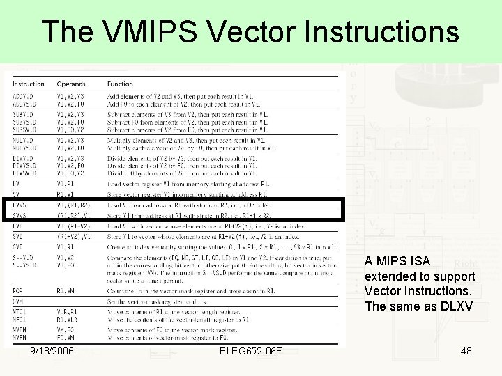
The VMIPS Vector Instructions A MIPS ISA extended to support Vector Instructions. The same as DLXV 9/18/2006 ELEG 652 -06 F 48

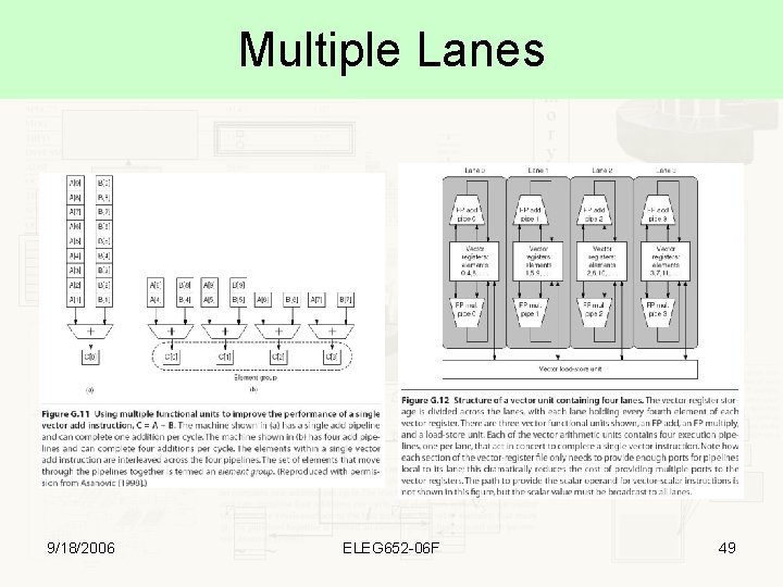
Multiple Lanes 9/18/2006 ELEG 652 -06 F 49

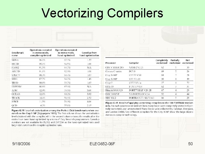
Vectorizing Compilers 9/18/2006 ELEG 652 -06 F 50

Topic 2 a Performance Analysis of Vector Architectures 9/18/2006 ELEG 652 -06 F 51

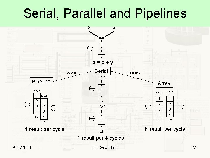
Serial, Parallel and Pipelines x y 1 2 3 4 z=x+y Overlap Serial Replicate x 1 y 1 Pipeline x 1 y 1 1 x 2 y 2 2 1 3 2 4 3 z 1 4 z 2 1 result per cycle 1 2 3 4 z 1 x 2 y 2 1 2 3 4 z 2 Array x 1 y 1 x 2 y 2 1 2 3 4 z 1 z 2 N result per cycle 1 result per 4 cycles 9/18/2006 ELEG 652 -06 F 52

Generic Performance Formula (R. Hockney & C. Jesshope 81) MFLOPS performance of the architecture with an infinite length vector The vector length needed to achieve half of the peak performance Vector length 9/18/2006 ELEG 652 -06 F 53

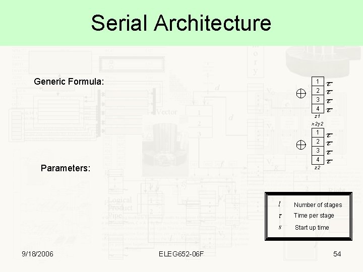
Serial Architecture Generic Formula: 1 2 3 4 z 1 x 2 y 2 1 2 3 4 Parameters: z 2 Number of stages Time per stage Start up time 9/18/2006 ELEG 652 -06 F 54

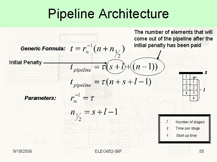
Pipeline Architecture The number of elements that will come out of the pipeline after the initial penalty has been paid Generic Formula: Initial Penalty 1 2 3 4 Parameters: s 1 2 3 4 l Number of stages Time per stage Start up time 9/18/2006 ELEG 652 -06 F 55

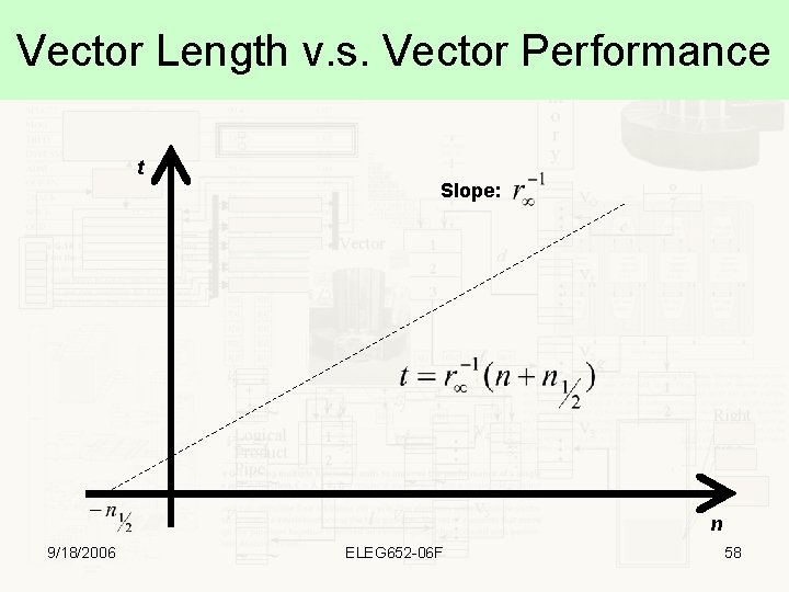
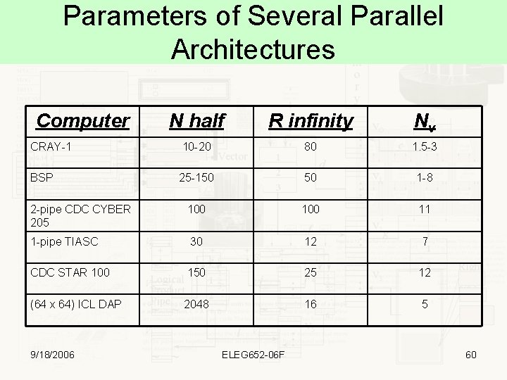
Thus … • The Asymptotic Performance Parameter – Memory Limited Peak Performance Factor. A scale factor applied to the performance of a particular architecture implemented with a particular technology. Equivalent to a serial processor with a 100% cache miss • The N half Parameter – The amount of parallelism that is presented in a given architecture. – Determined by a combination of vector unit startup and vector unit latency 9/18/2006 ELEG 652 -06 F 56

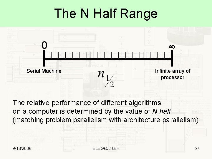
The N Half Range 0 ∞ Serial Machine Infinite array of processor The relative performance of different algorithms on a computer is determined by the value of N half (matching problem parallelism with architecture parallelism) 9/18/2006 ELEG 652 -06 F 57

Vector Length v. s. Vector Performance t Slope: n 9/18/2006 ELEG 652 -06 F 58

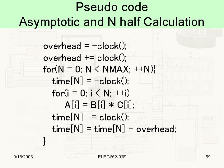
Pseudo code Asymptotic and N half Calculation overhead = -clock(); overhead += clock(); for(N = 0; N < NMAX; ++N){ time[N] = -clock(); for(i = 0; i < N; ++i) A[i] = B[i] * C[i]; time[N] += clock(); time[N] = time[N] - overhead; } 9/18/2006 ELEG 652 -06 F 59

Parameters of Several Parallel Architectures Computer N half R infinity Nv CRAY-1 10 -20 80 1. 5 -3 BSP 25 -150 50 1 -8 2 -pipe CDC CYBER 205 100 11 1 -pipe TIASC 30 12 7 CDC STAR 100 150 25 12 (64 x 64) ICL DAP 2048 16 5 9/18/2006 ELEG 652 -06 F 60

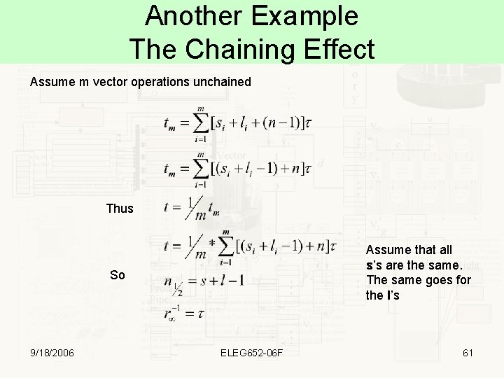
Another Example The Chaining Effect Assume m vector operations unchained Thus Assume that all s’s are the same. The same goes for the l’s So 9/18/2006 ELEG 652 -06 F 61

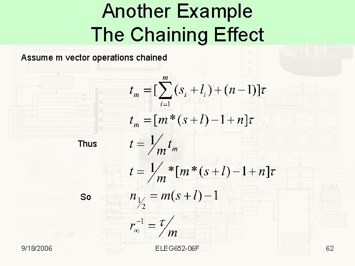
Another Example The Chaining Effect Assume m vector operations chained Thus So 9/18/2006 ELEG 652 -06 F 62

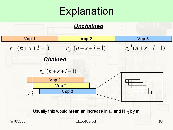
Explanation Unchained Vop 1 Vop 2 Vop 3 Chained s+l Vop 1 Vop 2 Vop 3 Usually this would mean an increase in r∞ and N 1/2 by m 9/18/2006 ELEG 652 -06 F 63

Topic 2 b Memory System Design in Vector Machines 9/18/2006 ELEG 652 -06 F 64

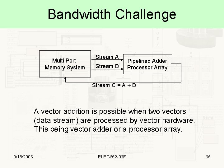
Bandwidth Challenge Multi Port Memory System Stream A Stream B Pipelined Adder Processor Array Stream C = A + B A vector addition is possible when two vectors (data stream) are processed by vector hardware. This being vector adder or a processor array. 9/18/2006 ELEG 652 -06 F 65

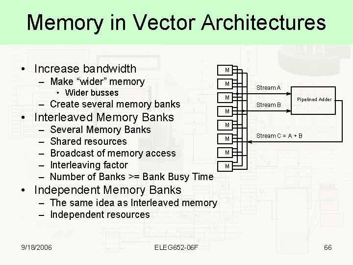
Memory in Vector Architectures • Increase bandwidth M – Make “wider” memory M • Wider busses – Create several memory banks • Interleaved Memory Banks – – – Several Memory Banks Shared resources Broadcast of memory access Interleaving factor Number of Banks >= Bank Busy Time Stream A M M Stream B Pipelined Adder M M Stream C = A + B M M • Independent Memory Banks – The same idea as Interleaved memory – Independent resources 9/18/2006 ELEG 652 -06 F 66

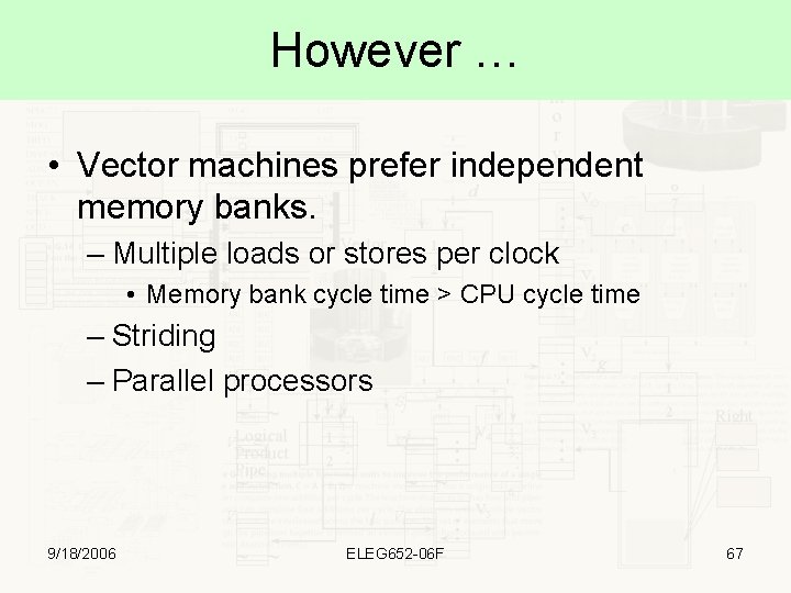
However … • Vector machines prefer independent memory banks. – Multiple loads or stores per clock • Memory bank cycle time > CPU cycle time – Striding – Parallel processors 9/18/2006 ELEG 652 -06 F 67

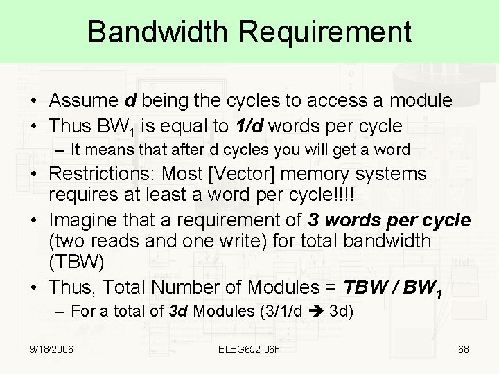
Bandwidth Requirement • Assume d being the cycles to access a module • Thus BW 1 is equal to 1/d words per cycle – It means that after d cycles you will get a word • Restrictions: Most [Vector] memory systems requires at least a word per cycle!!!! • Imagine that a requirement of 3 words per cycle (two reads and one write) for total bandwidth (TBW) • Thus, Total Number of Modules = TBW / BW 1 – For a total of 3 d Modules (3/1/d 3 d) 9/18/2006 ELEG 652 -06 F 68

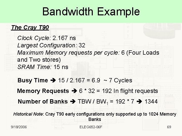
Bandwidth Example The Cray T 90 Clock Cycle: 2. 167 ns Largest Configuration: 32 Maximum Memory requests per cycle: 6 (Four Loads and Two stores) SRAM Time: 15 ns Busy Time 15 / 2. 167 = 6. 9 ~ 7 Cycles Memory Requests 6 * 32 = 192 In flight requests Number of Banks TBW / BW 1 = 192 * 7 1344 Historical Note: Cray T 90 early configurations only supported up to 1024 Memory Banks 9/18/2006 ELEG 652 -06 F 69

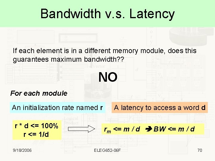
Bandwidth v. s. Latency If each element is in a different memory module, does this guarantees maximum bandwidth? ? NO For each module An initialization rate named r r * d <= 100% r <= 1/d 9/18/2006 A latency to access a word d rm <= m / d BW <= m / d ELEG 652 -06 F 70

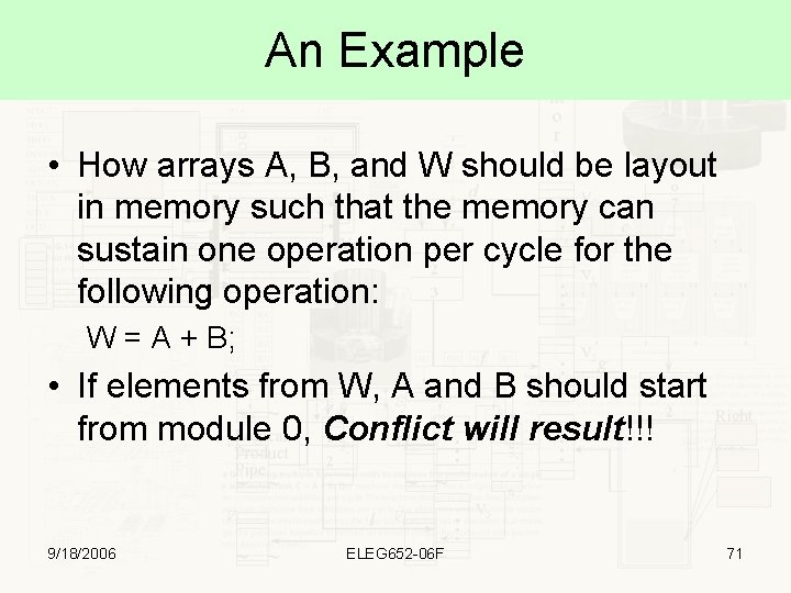
An Example • How arrays A, B, and W should be layout in memory such that the memory can sustain one operation per cycle for the following operation: W = A + B; • If elements from W, A and B should start from module 0, Conflict will result!!! 9/18/2006 ELEG 652 -06 F 71

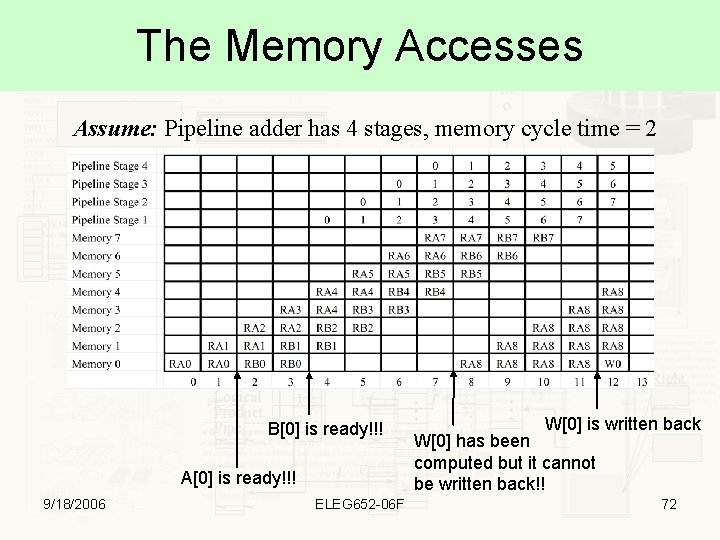
The Memory Accesses Assume: Pipeline adder has 4 stages, memory cycle time = 2 B[0] is ready!!! A[0] is ready!!! 9/18/2006 ELEG 652 -06 F W[0] is written back W[0] has been computed but it cannot be written back!! 72
![Another Memory Layout Modulo 0 A0 B6 W4 Modulo 1 A1 B7 W5 Modulo Another Memory Layout Modulo 0 A[0] B[6] W[4] Modulo 1 A[1] B[7] W[5] Modulo](https://slidetodoc.com/presentation_image_h2/45c4aaef8629856a2eddf10d98caa3cb/image-73.jpg)
Another Memory Layout Modulo 0 A[0] B[6] W[4] Modulo 1 A[1] B[7] W[5] Modulo 2 A[2] B[0] W[6] Modulo 3 A[3] B[1] W[7] Modulo 4 A[4] B[2] W[0] Modulo 5 A[5] B[3] W[1] Modulo 6 A[6] B[4] W[2] Modulo 7 A[7] B[5] W[3] 9/18/2006 ELEG 652 -06 F 73

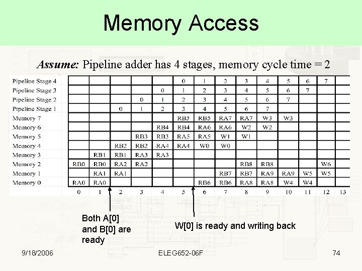
Memory Access Assume: Pipeline adder has 4 stages, memory cycle time = 2 Both A[0] and B[0] are ready 9/18/2006 W[0] is ready and writing back ELEG 652 -06 F 74

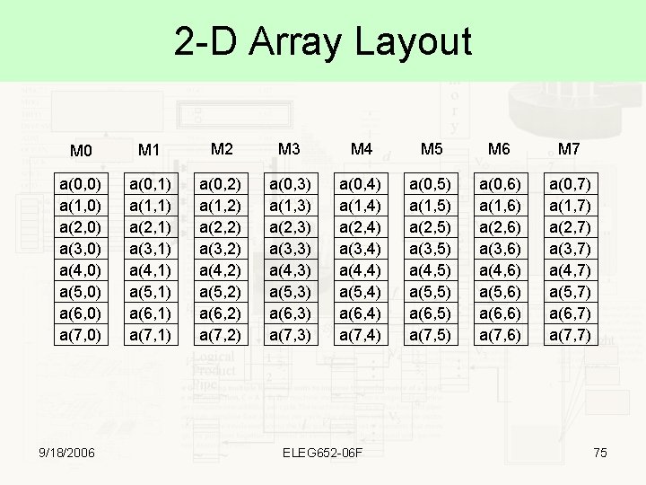
2 -D Array Layout M 0 M 1 M 2 M 3 M 4 M 5 M 6 M 7 a(0, 0) a(1, 0) a(2, 0) a(3, 0) a(4, 0) a(5, 0) a(6, 0) a(7, 0) a(0, 1) a(1, 1) a(2, 1) a(3, 1) a(4, 1) a(5, 1) a(6, 1) a(7, 1) a(0, 2) a(1, 2) a(2, 2) a(3, 2) a(4, 2) a(5, 2) a(6, 2) a(7, 2) a(0, 3) a(1, 3) a(2, 3) a(3, 3) a(4, 3) a(5, 3) a(6, 3) a(7, 3) a(0, 4) a(1, 4) a(2, 4) a(3, 4) a(4, 4) a(5, 4) a(6, 4) a(7, 4) a(0, 5) a(1, 5) a(2, 5) a(3, 5) a(4, 5) a(5, 5) a(6, 5) a(7, 5) a(0, 6) a(1, 6) a(2, 6) a(3, 6) a(4, 6) a(5, 6) a(6, 6) a(7, 6) a(0, 7) a(1, 7) a(2, 7) a(3, 7) a(4, 7) a(5, 7) a(6, 7) a(7, 7) 9/18/2006 ELEG 652 -06 F 75

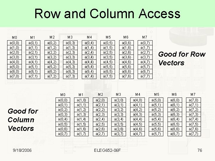
Row and Column Access M 0 a(0, 0) a(1, 0) a(2, 0) a(3, 0) a(4, 0) a(5, 0) a(6, 0) a(7, 0) M 1 M 2 M 3 M 4 M 5 M 6 M 7 a(0, 1) a(1, 1) a(2, 1) a(3, 1) a(4, 1) a(5, 1) a(6, 1) a(7, 1) a(0, 2) a(1, 2) a(2, 2) a(3, 2) a(4, 2) a(5, 2) a(6, 2) a(7, 2) a(0, 3) a(1, 3) a(2, 3) a(3, 3) a(4, 3) a(5, 3) a(6, 3) a(7, 3) a(0, 4) a(1, 4) a(2, 4) a(3, 4) a(4, 4) a(5, 4) a(6, 4) a(7, 4) a(0, 5) a(1, 5) a(2, 5) a(3, 5) a(4, 5) a(5, 5) a(6, 5) a(7, 5) a(0, 6) a(1, 6) a(2, 6) a(3, 6) a(4, 6) a(5, 6) a(6, 6) a(7, 6) a(0, 7) a(1, 7) a(2, 7) a(3, 7) a(4, 7) a(5, 7) a(6, 7) a(7, 7) Good for Column Vectors 9/18/2006 M 0 a(0, 0) a(0, 1) a(0, 2) a(0, 3) a(0, 4) a(0, 5) a(0, 6) a(0, 7) Good for Row Vectors M 1 M 2 M 3 M 4 M 5 M 6 M 7 a(1, 0) a(1, 1) a(1, 2) a(1, 3) a(1, 4) a(1, 5) a(1, 6) a(1, 7) a(2, 0) a(2, 1) a(2, 2) a(2, 3) a(2, 4) a(2, 5) a(2, 6) a(2, 7) a(3, 0) a(3, 1) a(3, 2) a(3, 3) a(3, 4) a(3, 5) a(3, 6) a(3, 7) a(4, 0) a(4, 1) a(4, 2) a(4, 3) a(4, 4) a(4, 5) a(4, 6) a(4, 7) a(5, 0) a(5, 1) a(5, 2) a(5, 3) a(5, 4) a(5, 5) a(5, 6) a(5, 7) a(6, 0) a(6, 1) a(6, 2) a(6, 3) a(6, 4) a(6, 5) a(6, 6) a(6, 7) a(7, 0) a(7, 1) a(7, 2) a(7, 3) a(7, 4) a(7, 5) a(7, 6) a(7, 7) ELEG 652 -06 F 76

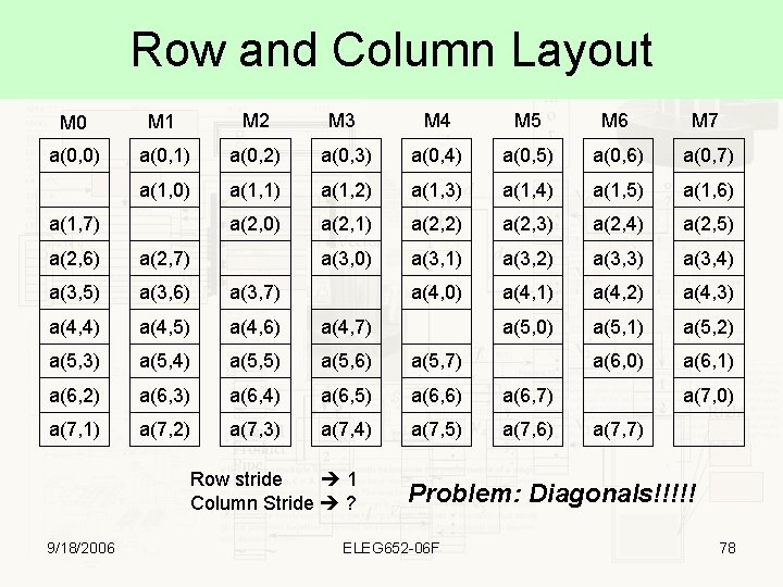
What to do? • Use algorithms that – Access row or column exclusively – Possible for some (i. e. LU decomposition) but not for others • Skew the matrix 9/18/2006 ELEG 652 -06 F 77

Row and Column Layout M 0 M 1 M 2 M 3 M 4 M 5 M 6 M 7 a(0, 0) a(0, 1) a(0, 2) a(0, 3) a(0, 4) a(0, 5) a(0, 6) a(0, 7) a(1, 0) a(1, 1) a(1, 2) a(1, 3) a(1, 4) a(1, 5) a(1, 6) a(2, 0) a(2, 1) a(2, 2) a(2, 3) a(2, 4) a(2, 5) a(3, 0) a(3, 1) a(3, 2) a(3, 3) a(3, 4) a(4, 0) a(4, 1) a(4, 2) a(4, 3) a(5, 0) a(5, 1) a(5, 2) a(6, 0) a(6, 1) a(1, 7) a(2, 6) a(2, 7) a(3, 5) a(3, 6) a(3, 7) a(4, 4) a(4, 5) a(4, 6) a(4, 7) a(5, 3) a(5, 4) a(5, 5) a(5, 6) a(5, 7) a(6, 2) a(6, 3) a(6, 4) a(6, 5) a(6, 6) a(6, 7) a(7, 1) a(7, 2) a(7, 3) a(7, 4) a(7, 5) a(7, 6) Row stride 1 Column Stride ? 9/18/2006 a(7, 0) a(7, 7) Problem: Diagonals!!!!! ELEG 652 -06 F 78

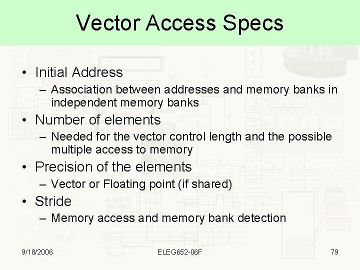
Vector Access Specs • Initial Address – Association between addresses and memory banks in independent memory banks • Number of elements – Needed for the vector control length and the possible multiple access to memory • Precision of the elements – Vector or Floating point (if shared) • Stride – Memory access and memory bank detection 9/18/2006 ELEG 652 -06 F 79

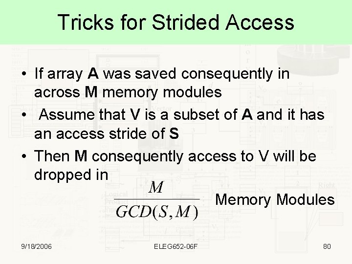
Tricks for Strided Access • If array A was saved consequently in across M memory modules • Assume that V is a subset of A and it has an access stride of S • Then M consequently access to V will be dropped in Memory Modules 9/18/2006 ELEG 652 -06 F 80

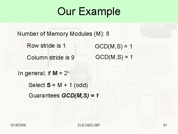
Our Example Number of Memory Modules (M): 8 Row stride is 1 GCD(M, S) = 1 Column stride is 9 GCD(M, S) = 1 In general, if M = 2 k Select S = M + 1 (odd) Guarantees GCD(M, S) = 1 9/18/2006 ELEG 652 -06 F 81

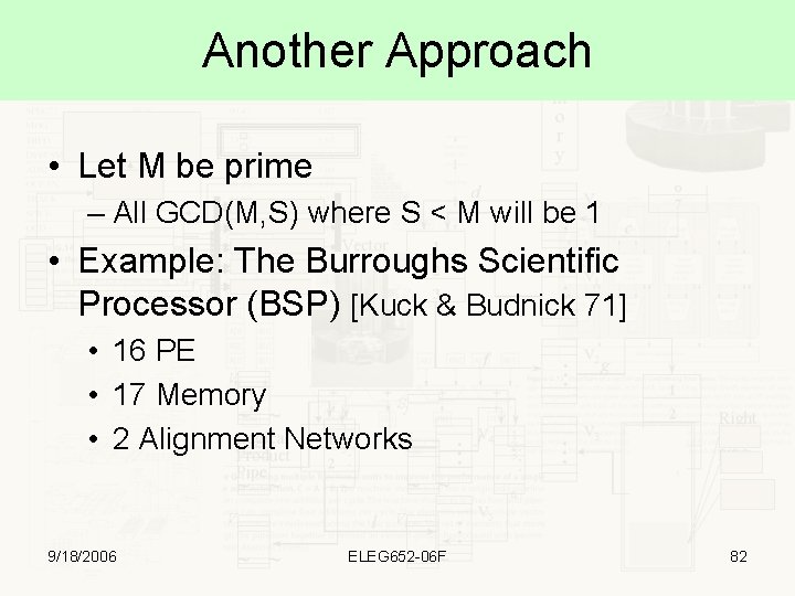
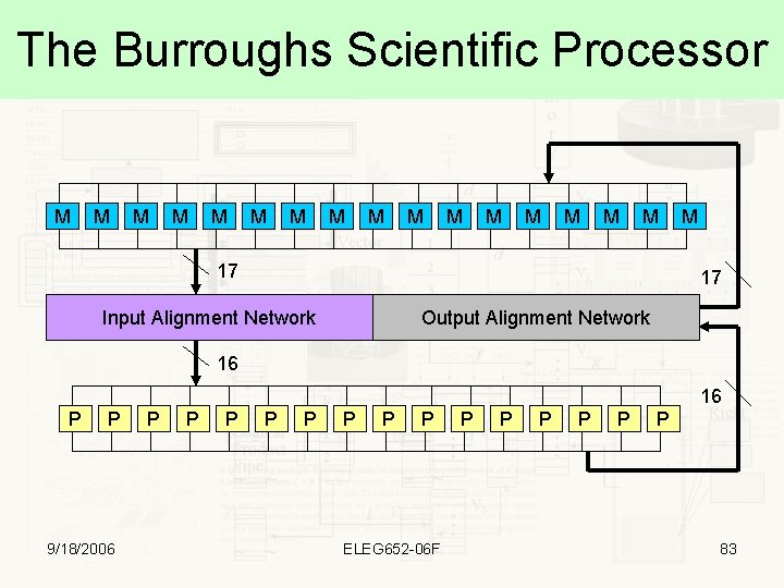
Another Approach • Let M be prime – All GCD(M, S) where S < M will be 1 • Example: The Burroughs Scientific Processor (BSP) [Kuck & Budnick 71] • 16 PE • 17 Memory • 2 Alignment Networks 9/18/2006 ELEG 652 -06 F 82

The Burroughs Scientific Processor M M M M 17 M 17 Input Alignment Network Output Alignment Network 16 16 P P 9/18/2006 P P P P ELEG 652 -06 F P P P 83

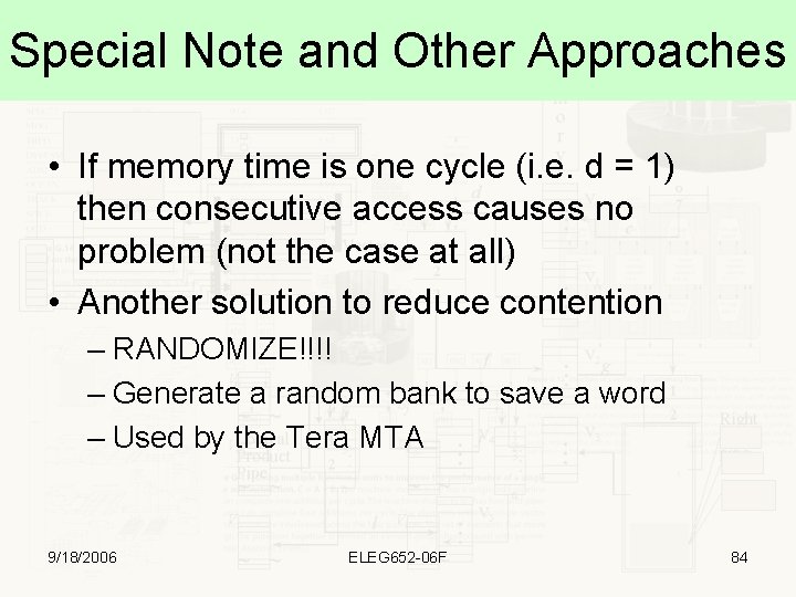
Special Note and Other Approaches • If memory time is one cycle (i. e. d = 1) then consecutive access causes no problem (not the case at all) • Another solution to reduce contention – RANDOMIZE!!!! – Generate a random bank to save a word – Used by the Tera MTA 9/18/2006 ELEG 652 -06 F 84

Questions? ? Comments? ? 9/18/2006 ELEG 652 -06 F 85

Bibliography • Stork, Christian. “Exploring the Tera MTA by Example” May 10, 2000 • Cray 1 Computer System Hardware Reference Manual • Koopman, Phillips, “ 17. Vector Performance”, November 9, 1998. A lecture in Carnegie Mellon University 9/18/2006 ELEG 652 -06 F 86

Side Note 2 Gordon Bells’ Rules for Supercomputers • Put attention to performance • Orchestrate your resources • Scalars are bottlenecks – Plan your scalar section very carefully • Use existing (affordable) technology to provide a peak vector performance – Vector Performance: Bandwidth and vector register capacity. – Rule of Thumb: At least two results per cycle • Do not ignore expensive ops – Division are uncommon but they are used!!!! • Design to Market – Create something to brag about 9/18/2006 ELEG 652 -06 F 87

Side Note 2 Gordon Bells’ Rules for Supercomputers • 10 ~ 7 – Support around two extra bits of addressing per 3 years (10 years ~= 7 bits) • Increase Productivity • Stand on the shoulders of giants • Pipeline your design – Design for one and then other… • Give you enough lay time in your schedule for unexpected – Beware of Murphy’s Laws!!!! 9/18/2006 ELEG 652 -06 F 88