The World Leader in HighPerformance Signal Processing Solutions

- Slides: 44

The World Leader in High-Performance Signal Processing Solutions Data Conversion Fundamentals Digital-Analog Converters Online Seminar Winter 2002

The World Leader in High-Performance Signal Processing Solutions Introduction to D/A Converters

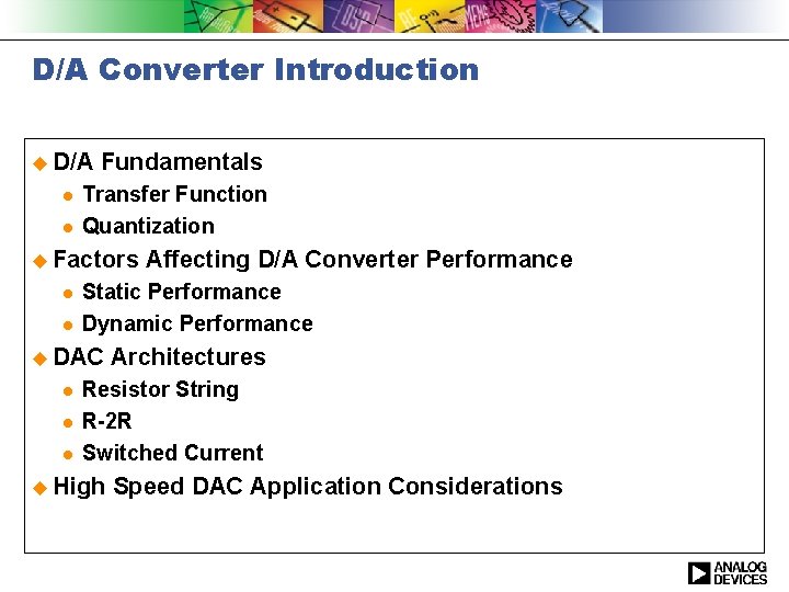
D/A Converter Introduction u D/A l l Fundamentals Transfer Function Quantization u Factors l l Static Performance Dynamic Performance u DAC l l l Affecting D/A Converter Performance Architectures Resistor String R-2 R Switched Current u High Speed DAC Application Considerations

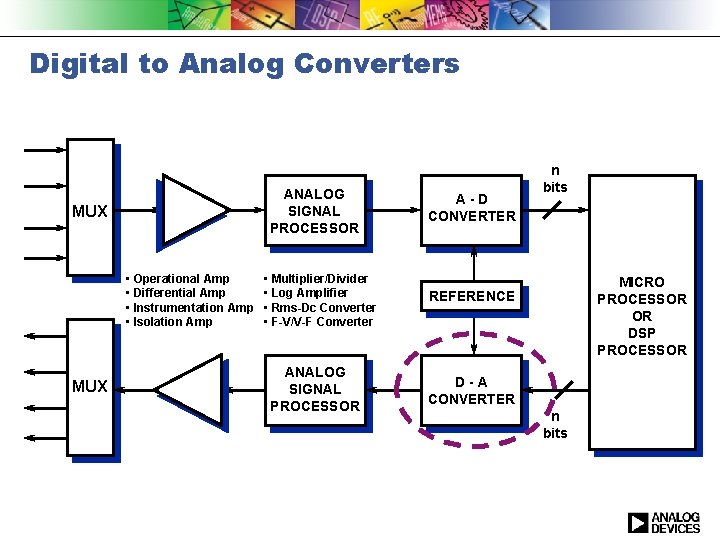
Digital to Analog Converters ANALOG SIGNAL PROCESSOR MUX • Operational Amp • Differential Amp • Instrumentation Amp • Isolation Amp MUX • Multiplier/Divider • Log Amplifier • Rms-Dc Converter • F-V/V-F Converter ANALOG SIGNAL PROCESSOR A-D CONVERTER n bits MICRO PROCESSOR OR DSP PROCESSOR REFERENCE D-A CONVERTER n bits

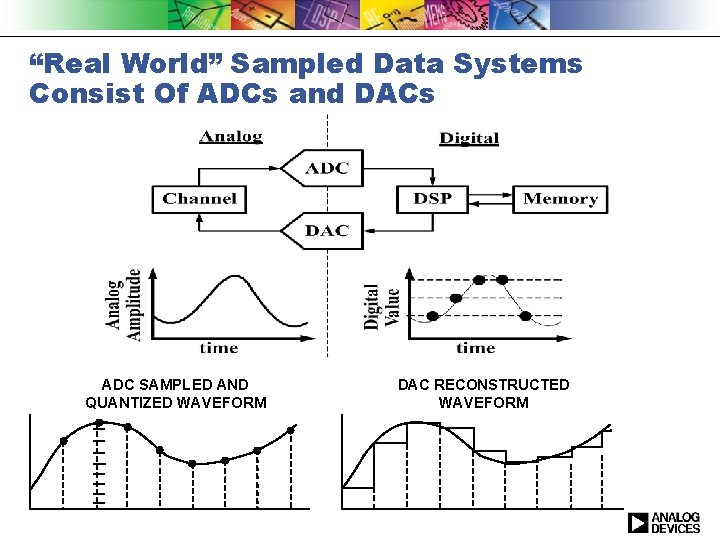
“Real World” Sampled Data Systems Consist Of ADCs and DACs ADC SAMPLED AND QUANTIZED WAVEFORM DAC RECONSTRUCTED WAVEFORM

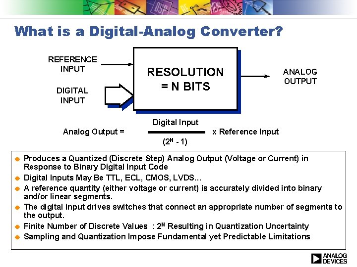
What is a Digital-Analog Converter? REFERENCE INPUT DIGITAL INPUT RESOLUTION = N BITS ANALOG OUTPUT Digital Input Analog Output = x Reference Input (2 N u u u - 1) Produces a Quantized (Discrete Step) Analog Output (Voltage or Current) in Response to Binary Digital Input Code Digital Inputs May Be TTL, ECL, CMOS, LVDS… A reference quantity (either voltage or current) is accurately divided into binary and/or linear segments. The digital input drives switches that connect an appropriate number of segments to the output. Finite Number of Discrete Values : 2 N Resulting in Quantization Uncertainty Sampling and Quantization Impose Fundamental yet Predictable Limitations

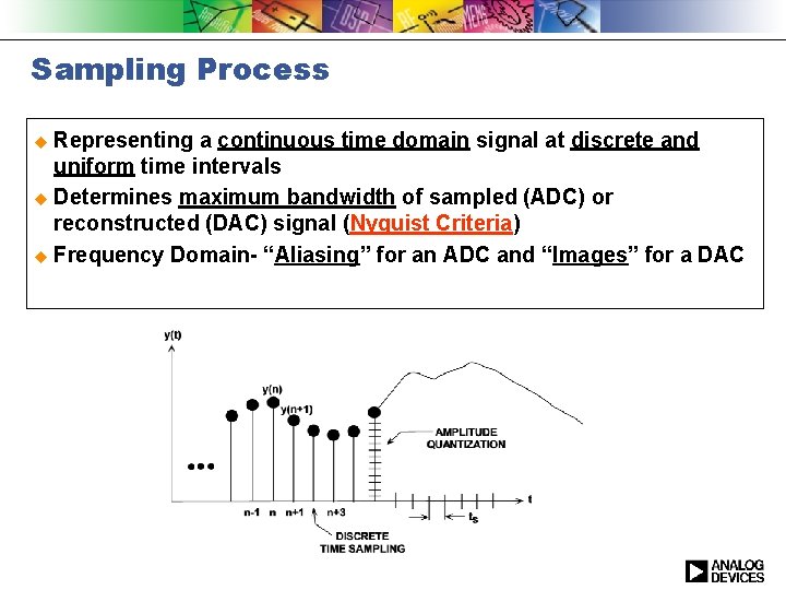
Sampling Process u Representing a continuous time domain signal at discrete and uniform time intervals u Determines maximum bandwidth of sampled (ADC) or reconstructed (DAC) signal (Nyquist Criteria) u Frequency Domain- “Aliasing” for an ADC and “Images” for a DAC

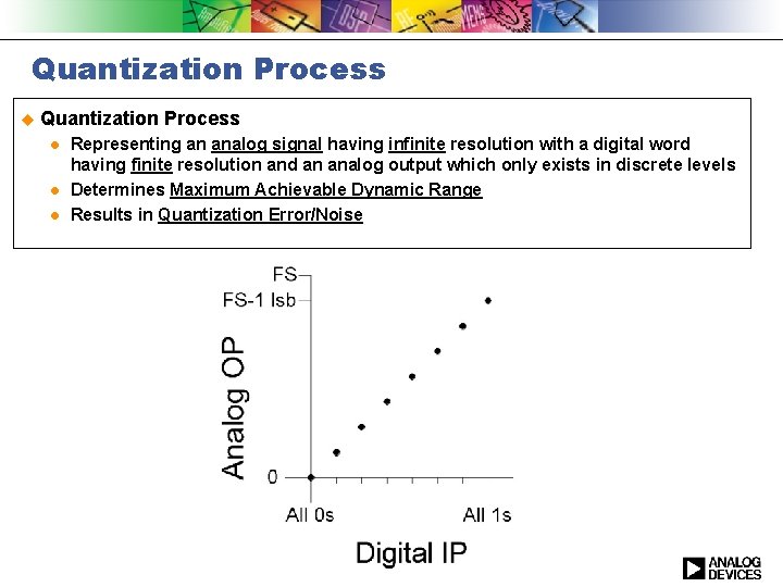
Quantization Process u Quantization Process l l l Representing an analog signal having infinite resolution with a digital word having finite resolution and an analog output which only exists in discrete levels Determines Maximum Achievable Dynamic Range Results in Quantization Error/Noise

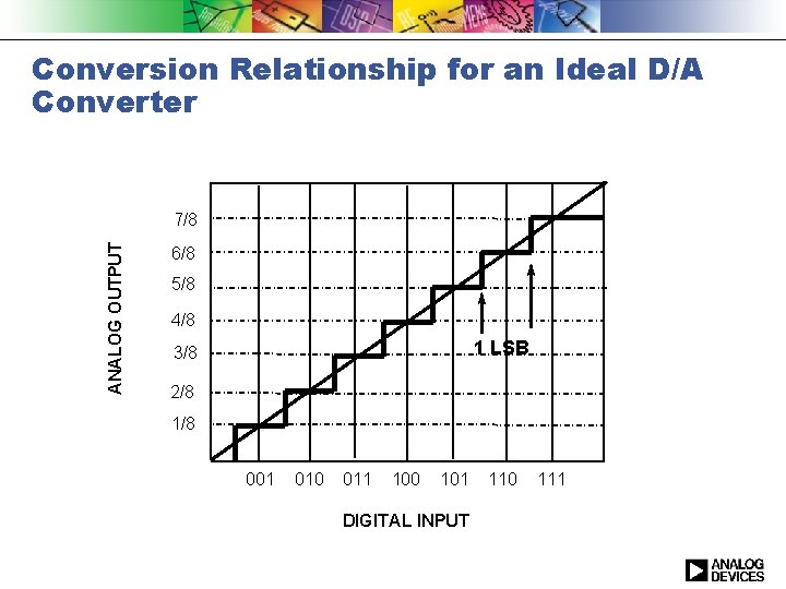
Conversion Relationship for an Ideal D/A Converter ANALOG OUTPUT 7/8 6/8 5/8 4/8 1 LSB 3/8 2/8 1/8 001 010 011 100 101 DIGITAL INPUT 110 111

DAC Resolution, LSBs and More. . .

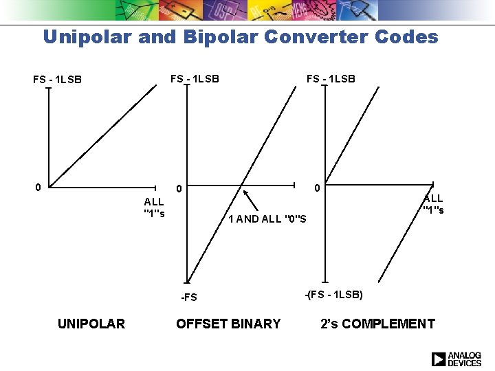
Unipolar and Bipolar Converter Codes FS - 1 LSB 0 0 ALL "1"s 1 AND ALL "0"S -FS UNIPOLAR OFFSET BINARY ALL "1"s -(FS - 1 LSB) 2’s COMPLEMENT

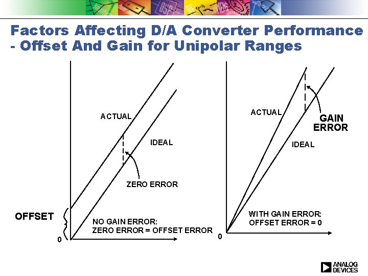
Factors Affecting D/A Converter Performance - Offset And Gain for Unipolar Ranges ACTUAL IDEAL GAIN ERROR IDEAL ZERO ERROR OFFSET NO GAIN ERROR: ZERO ERROR = OFFSET ERROR 0 WITH GAIN ERROR: OFFSET ERROR = 0 0

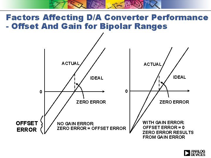
Factors Affecting D/A Converter Performance - Offset And Gain for Bipolar Ranges ACTUAL IDEAL 0 0 ZERO ERROR OFFSET ERROR NO GAIN ERROR: ZERO ERROR = OFFSET ERROR ZERO ERROR WITH GAIN ERROR: OFFSET ERROR = 0 ZERO ERROR RESULTS FROM GAIN ERROR

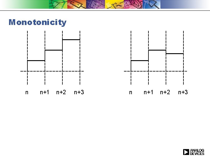
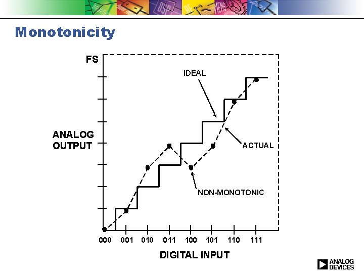
DC Specifications (DNL & Montonicity) u Differential Non-Linearity (DNL) is the deviation of an actual step size from the ideal 1 LSB step. u DNL error results in smaller or larger step sizes than ideal u DNL error esults in additive noise/spurs beyond the effects of quantization u A DAC Is Monotonic If Its Output Increases or Remains the Same for an Increment in the Digital Code u Conversely, a DAC Is Non-Monotonic If the Output Decreases for an Increment in the Digital Code

Monotonicity n n+1 n+2 n+3

Monotonicity FS IDEAL ANALOG OUTPUT ACTUAL NON-MONOTONIC 000 001 010 011 100 101 110 DIGITAL INPUT 111

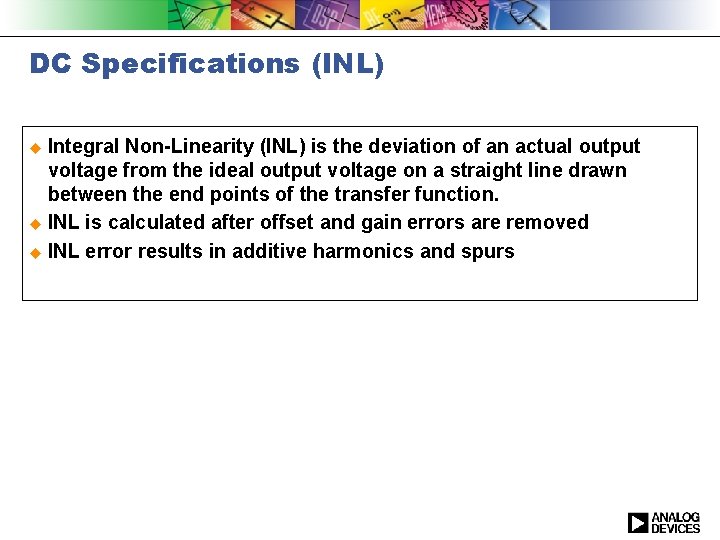
DC Specifications (INL) u Integral Non-Linearity (INL) is the deviation of an actual output voltage from the ideal output voltage on a straight line drawn between the end points of the transfer function. u INL is calculated after offset and gain errors are removed u INL error results in additive harmonics and spurs

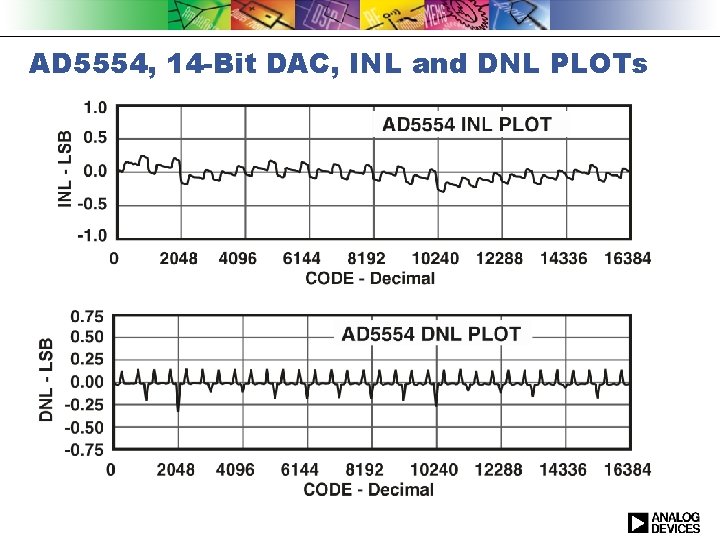
AD 5554, 14 -Bit DAC, INL and DNL PLOTs

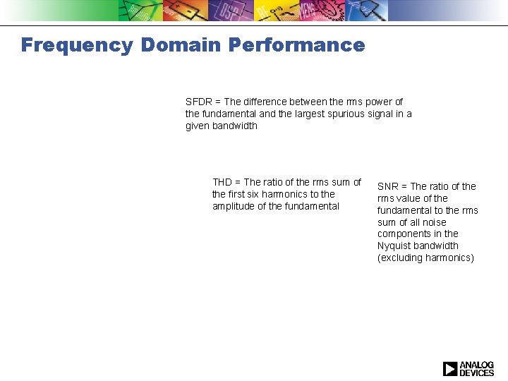
Frequency Domain Performance SFDR = The difference between the rms power of the fundamental and the largest spurious signal in a given bandwidth THD = The ratio of the rms sum of the first six harmonics to the amplitude of the fundamental SNR = The ratio of the rms value of the fundamental to the rms sum of all noise components in the Nyquist bandwidth (excluding harmonics)

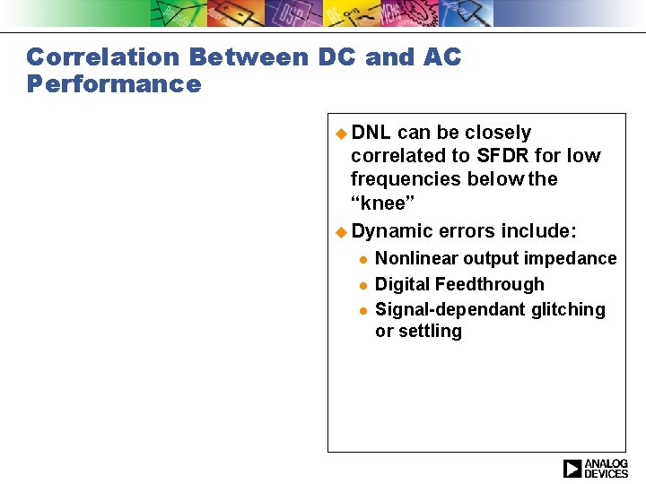
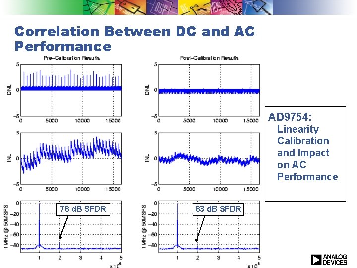
Correlation Between DC and AC Performance u DNL can be closely correlated to SFDR for low frequencies below the “knee” u Dynamic errors include: l l l Nonlinear output impedance Digital Feedthrough Signal-dependant glitching or settling

Correlation Between DC and AC Performance AD 9754: Linearity Calibration and Impact on AC Performance 78 d. B SFDR 83 d. B SFDR

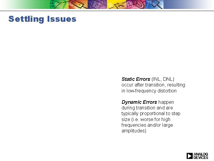
Settling Issues Static Errors (INL, DNL) occur after transition, resulting in low-frequency distortion Dynamic Errors happen during transition and are typically proportional to step size (i. e. worse for high frequencies and/or large amplitudes)

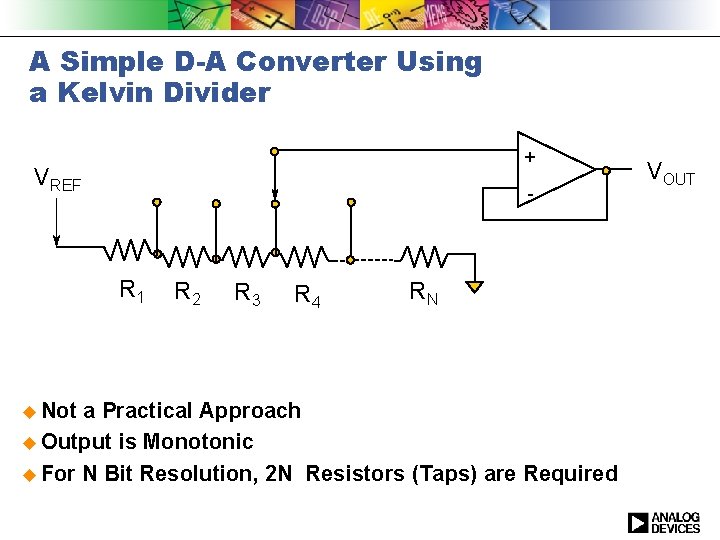
A Simple D-A Converter Using a Kelvin Divider + VREF - R 1 u Not R 2 R 3 R 4 RN a Practical Approach u Output is Monotonic u For N Bit Resolution, 2 N Resistors (Taps) are Required VOUT

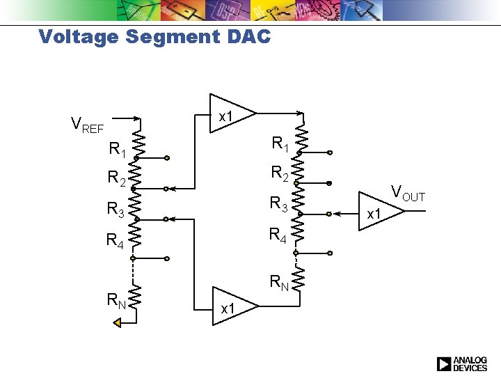
Voltage Segment DAC x 1 VREF R 1 R 2 R 3 R 4 RN RN x 1 VOUT x 1

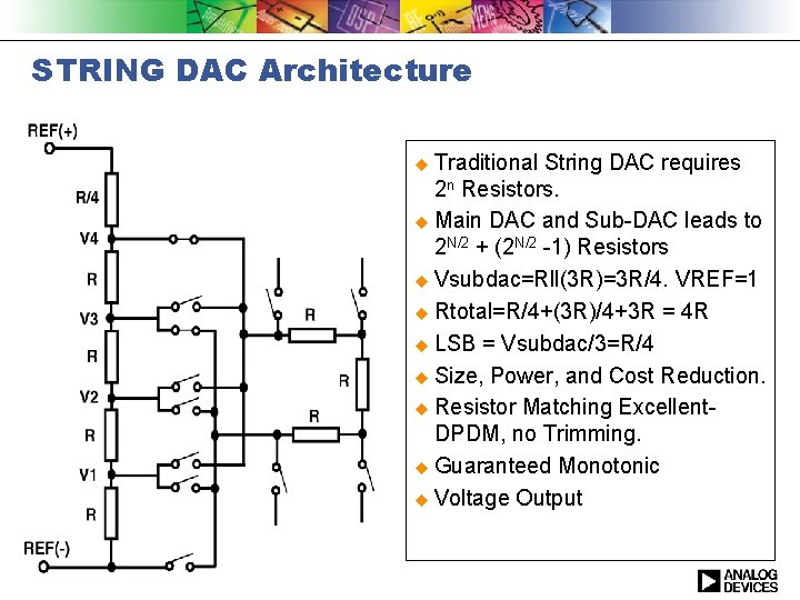
STRING DAC Architecture u Traditional String DAC requires 2 n Resistors. u Main DAC and Sub-DAC leads to 2 N/2 + (2 N/2 -1) Resistors u Vsubdac=Rll(3 R)=3 R/4. VREF=1 u Rtotal=R/4+(3 R)/4+3 R = 4 R u LSB = Vsubdac/3=R/4 u Size, Power, and Cost Reduction. u Resistor Matching Excellent. DPDM, no Trimming. u Guaranteed Monotonic u Voltage Output

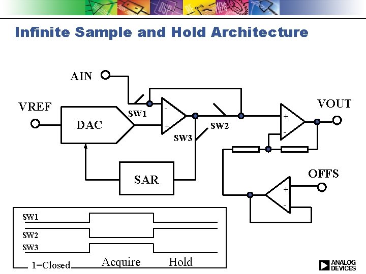
Infinite Sample and Hold Architecture AIN VREF DAC SW 1 VOUT + SW 2 SW 3 + - OFFS SAR + - SW 1 SW 2 SW 3 1=Closed Acquire Hold

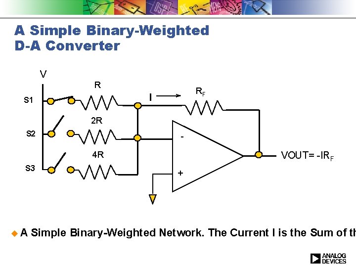
A Simple Binary-Weighted D-A Converter V R RF I S 1 2 R S 2 4 R u. A + S 3 VOUT= -IRF Simple Binary-Weighted Network. The Current I is the Sum of th

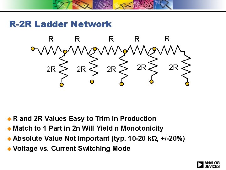
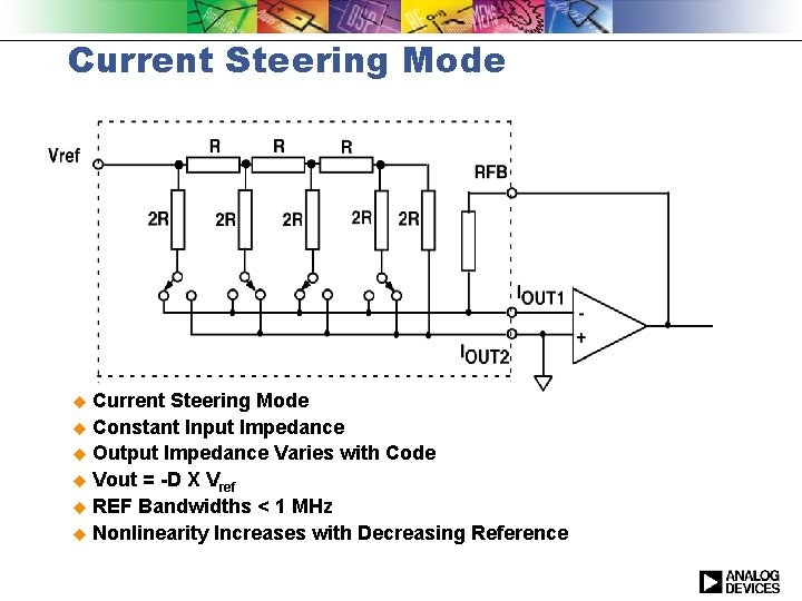
R-2 R Ladder Network u. R R 2 R 2 R 2 R and 2 R Values Easy to Trim in Production u Match to 1 Part in 2 n Will Yield n Monotonicity u Absolute Value Not Important (typ. 10 -20 k. W, +/-20%) u Voltage vs. Current Switching Mode

Current Steering Mode u Constant Input Impedance u Output Impedance Varies with Code u Vout = -D X Vref u REF Bandwidths < 1 MHz u Nonlinearity Increases with Decreasing Reference u

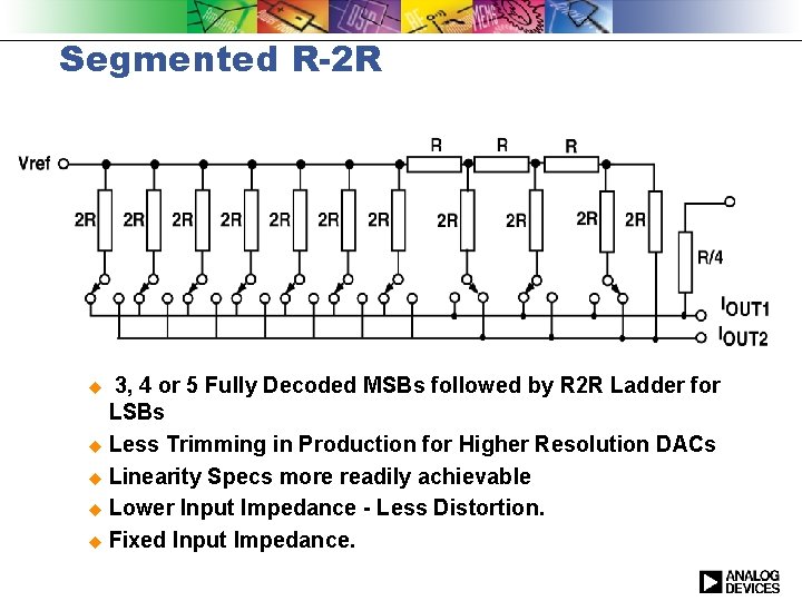
Segmented R-2 R 3, 4 or 5 Fully Decoded MSBs followed by R 2 R Ladder for LSBs u Less Trimming in Production for Higher Resolution DACs u Linearity Specs more readily achievable u Lower Input Impedance - Less Distortion. u Fixed Input Impedance. u

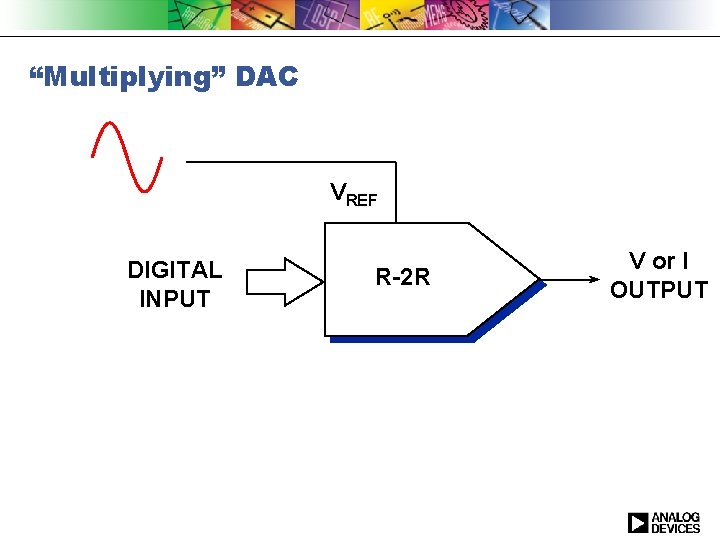
“Multiplying” DAC VREF DIGITAL INPUT R-2 R V or I OUTPUT

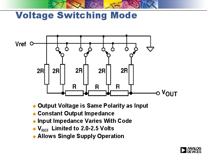
Voltage Switching Mode u Output Voltage is Same Polarity as Input u Constant Output Impedance u Input Impedance Varies With Code u VREF Limited to 2. 0 -2. 5 Volts u Allows Single Supply Operation

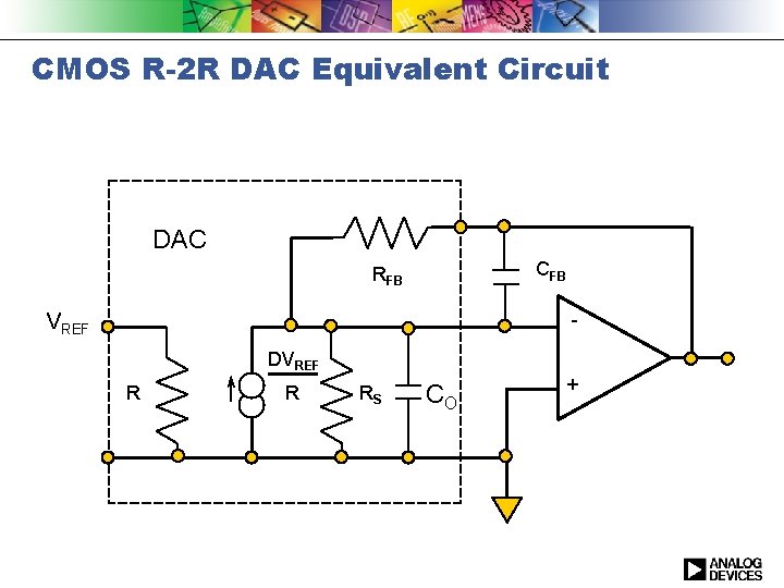
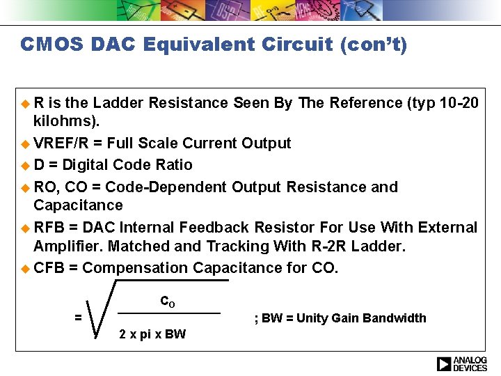
CMOS R-2 R DAC Equivalent Circuit DAC CFB RFB VREF DVREF R RS CO + R

CMOS DAC Equivalent Circuit (con’t) u. R is the Ladder Resistance Seen By The Reference (typ 10 -20 kilohms). u VREF/R = Full Scale Current Output u D = Digital Code Ratio u RO, CO = Code-Dependent Output Resistance and Capacitance u RFB = DAC Internal Feedback Resistor For Use With External Amplifier. Matched and Tracking With R-2 R Ladder. u CFB = Compensation Capacitance for CO. CO = ; BW = Unity Gain Bandwidth 2 x pi x BW

Bipolar Switched Current DAC u Good device matching results in good DC performance u Device scaling difficult, requires R-2 R for higher resolution u Typically higher power, can’t integrate Digital Signal Processing

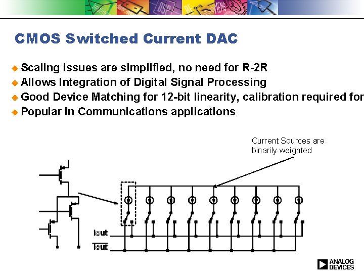
CMOS Switched Current DAC u Scaling issues are simplified, no need for R-2 R u Allows Integration of Digital Signal Processing u Good Device Matching for 12 -bit linearity, calibration required for u Popular in Communications applications Current Sources are binarily weighted

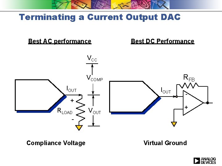
Terminating a Current Output DAC Best AC performance Best DC Performance VCC RFB IOUT RLOAD - Compliance Voltage VOUT + + - VCOMP Virtual Ground

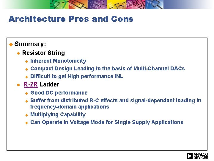
Architecture Pros and Cons u Summary: l Resistor String u u u l Inherent Monotonicity Compact Design Leading to the basis of Multi-Channel DACs Difficult to get High performance INL R-2 R Ladder u u Good DC performance Suffer from distributed R-C effects and signal-dependant loading in frequency-domain applications Multiplying Capability Can Operate in Voltage Mode for Single Supply Applications

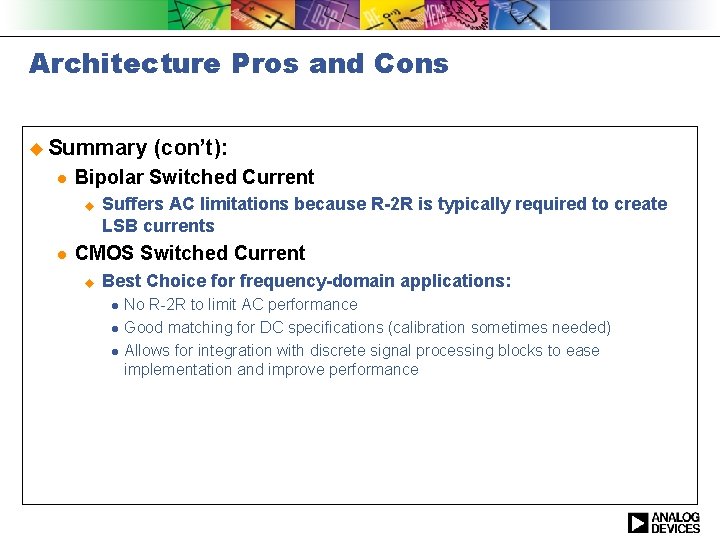
Architecture Pros and Cons u Summary l Bipolar Switched Current u l (con’t): Suffers AC limitations because R-2 R is typically required to create LSB currents CMOS Switched Current u Best Choice for frequency-domain applications: l l l No R-2 R to limit AC performance Good matching for DC specifications (calibration sometimes needed) Allows for integration with discrete signal processing blocks to ease implementation and improve performance

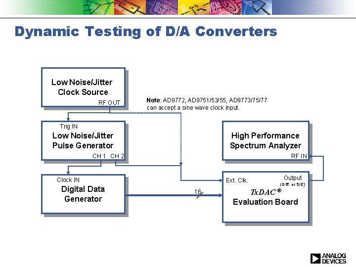
Dynamic Testing of D/A Converters Low Noise/Jitter Clock Source RF OUT Note: AD 9772, AD 9751/53/55, AD 9773/75/77 can accept a sine wave clock input. Trig IN Low Noise/Jitter Pulse Generator High Performance Spectrum Analyzer RF IN CH 1 CH 2 Clock IN Digital Data Generator Ext. Clk. 16 Output (Diff. or S/E) Tx. DAC ® Evaluation Board

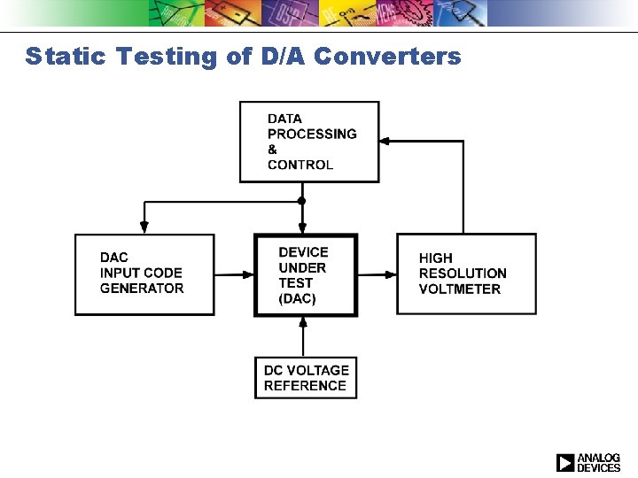
Static Testing of D/A Converters

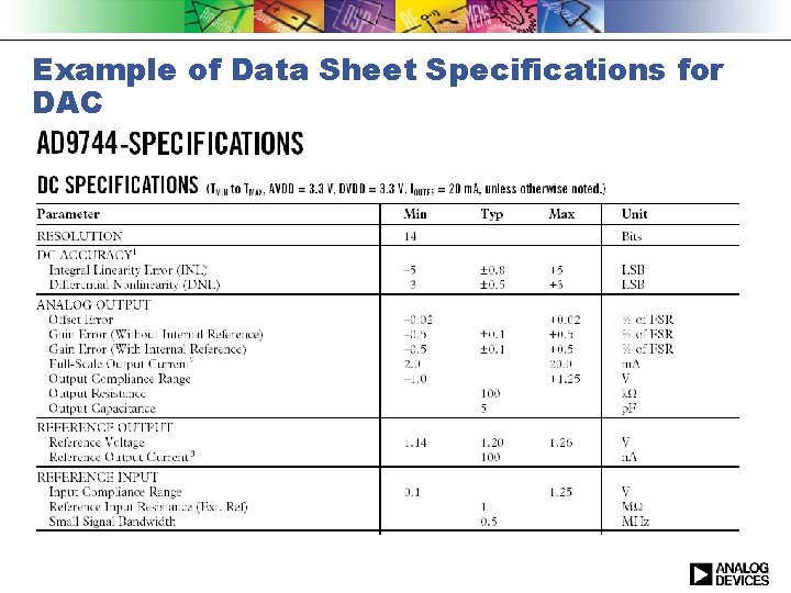
Example of Data Sheet Specifications for DAC

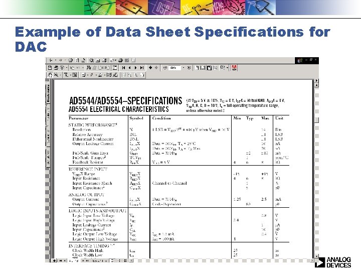
Example of Data Sheet Specifications for DAC

For complete information on the World’s most extensive line of D/A converters visit WWW. ANALOG. COM