The World Leader in HighPerformance Signal Processing Solutions
- Slides: 27

The World Leader in High-Performance Signal Processing Solutions Design a Clock Distribution for a WCDMA Transceiver System CSNDSP 2006 Session: B. 11 Systems - Simulators Presenter: Dimitrios Efstathiou July 20 th, 2006

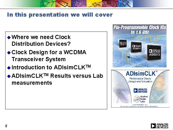
In this presentation we will cover u Where we need Clock Distribution Devices? u Clock Design for a WCDMA Transceiver System u Introduction to ADIsim. CLKTM u ADIsim. CLKTM Results versus Lab measurements 2

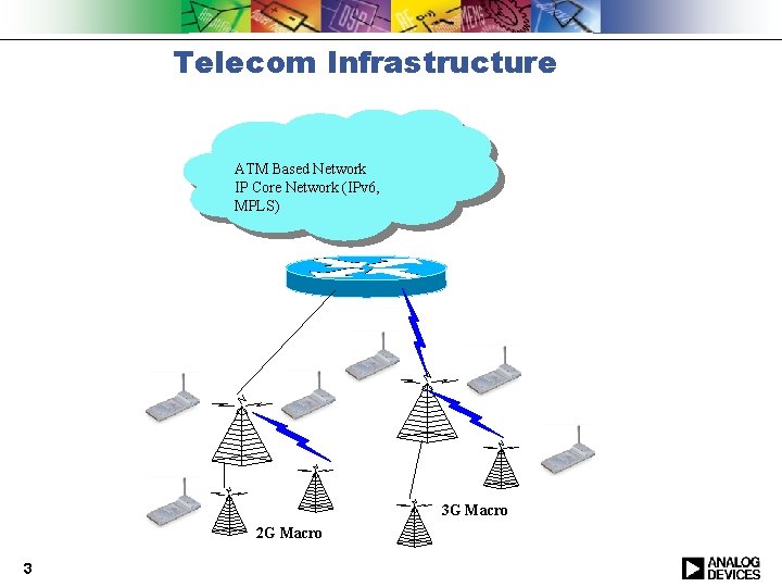
Telecom Infrastructure ATM Based Network IP Core Network (IPv 6, MPLS) 3 G Macro 2 G Macro 3

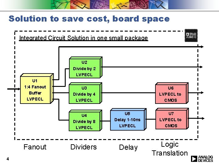
Solution to save cost, board space Integrated Circuit Solution in one small package U 2 Divide by 2 LVPECL U 1 1: 4 Fanout Buffer LVPECL Fanout 4 U 3 Divide by 4 LVPECL U 6 LVPECL to CMOS U 4 Divide by 8 LVPECL U 5 Delay 1 -10 ns LVPECL U 7 LVPECL to CMOS Dividers Delay Logic Translation

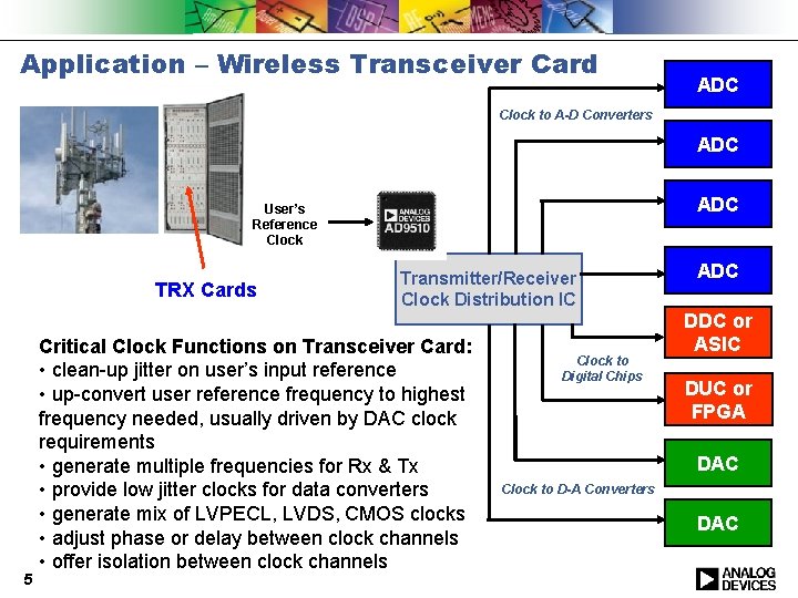
Application – Wireless Transceiver Card ADC Clock to A-D Converters ADC User’s Reference Clock TRX Cards 5 Transmitter/Receiver Clock Distribution IC Critical Clock Functions on Transceiver Card: • clean-up jitter on user’s input reference • up-convert user reference frequency to highest frequency needed, usually driven by DAC clock requirements • generate multiple frequencies for Rx & Tx • provide low jitter clocks for data converters • generate mix of LVPECL, LVDS, CMOS clocks • adjust phase or delay between clock channels • offer isolation between clock channels Clock to Digital Chips ADC DDC or ASIC DUC or FPGA DAC Clock to D-A Converters DAC

Transceiver clock design using ADIsim. CLK™ 6

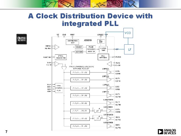
A Clock Distribution Device with integrated PLL VCO LF 7

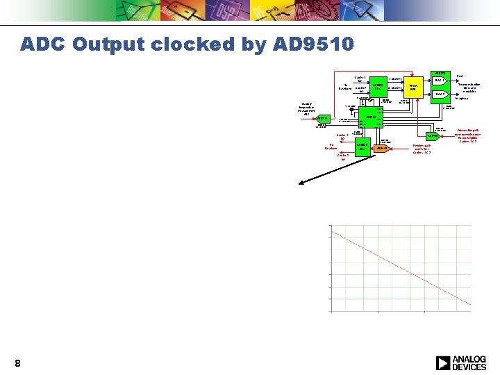
ADC Output clocked by AD 9510 AD 9779 Carrier 1 I/Q Tx Baseband I-channel Carrier 2 I/Q AD 6633 DUC CMOS 76. 80 MHz To reconstruction filters and modulator Imaginary LVPECL 307. 20 MHz LVDS 614. 40 MHz 19. 20 MHz OUT 6 OUT 0 AD 9215 LVEPCL 19. 20 MHz AD 9510 OUT 1 OUT 4 OUT 5 CMOS 30. 72 MHz Carrier 1 I/Q Rx Baseband OUT 7 OUT 2 OUT 3 LVDS 102. 40 MHz AD 6636 DDC Carrier 2 I/Q 8 FPGA DPD DAC 2 614. 40 MHz Auxilary temperature measurement ADC Q-channel Real DAC 1 LVPECL 153. 60 MHz AD 9430 LVPECL 102. 40 MHz AD 9445 Receiver path from Mixer Carriers 1 & 2 Observation path down-converted from Power Amplifier Carriers 1 & 2

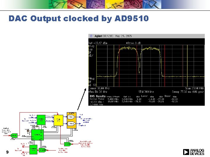
DAC Output clocked by AD 9510 AD 9779 Carrier 1 I/Q Tx Baseband Carrier 2 I/Q I-channel AD 6633 DUC CMOS 76. 80 MHz To reconstruction filters and modulator Imaginary LVPECL 307. 20 MHz LVDS 614. 40 MHz 19. 20 MHz OUT 6 OUT 0 AD 9215 LVEPCL 19. 20 MHz AD 9510 OUT 1 OUT 4 CMOS 30. 72 MHz OUT 5 Carrier 1 I/Q 9 FPGA DPD DAC 2 614. 40 MHz Auxilary temperature measurement ADC Q-channel Real DAC 1 Rx Baseband Carrier 2 I/Q OUT 7 OUT 2 OUT 3 LVPECL 153. 60 MHz LVDS 102. 40 MHz AD 9430 LVPECL 102. 40 MHz AD 6636 DDC AD 9445 Receiver path from Mixer Carriers 1 & 2 Observation path down-converted from Power Amplifier Carriers 1 & 2

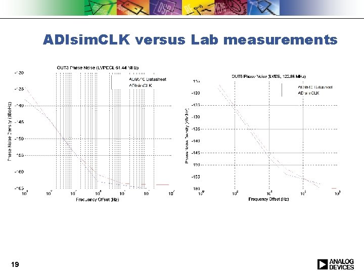
ADIsim. CLK™ ADIsim. CLK is a powerful and flexible tool. It can help a user design high performance clocking systems using low-jitter clock chips. ADIsim. CLK phase noise simulations match the product information sheet typical values within ~2 d. B. Timing simulations align well with product information sheet typical values. 10

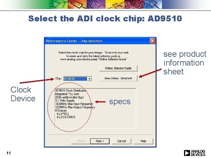
Select the ADI clock chip: AD 9510 see product information sheet Clock Device 11 specs

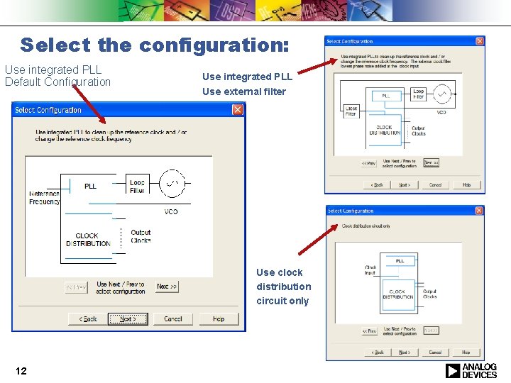
Select the configuration: Use integrated PLL Default Configuration Use integrated PLL Use external filter Use clock distribution circuit only 12

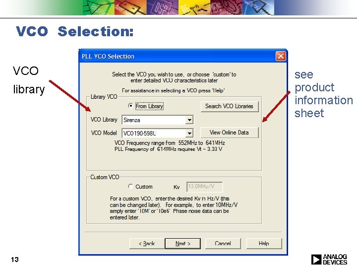
VCO Selection: VCO library 13 see product information sheet

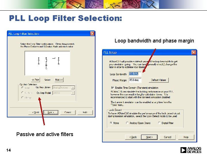
PLL Loop Filter Selection: Loop bandwidth and phase margin Passive and active filters 14

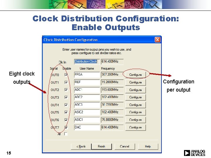
Clock Distribution Configuration: Enable Outputs Eight clock outputs Configuration per output 15

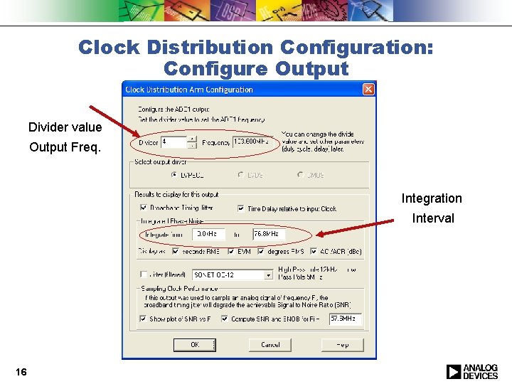
Clock Distribution Configuration: Configure Output Divider value Output Freq. Integration Interval 16

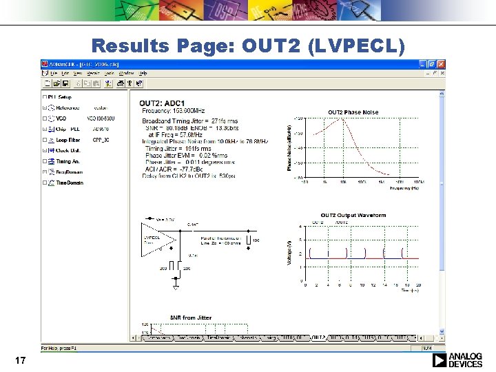
Results Page: OUT 2 (LVPECL) 17

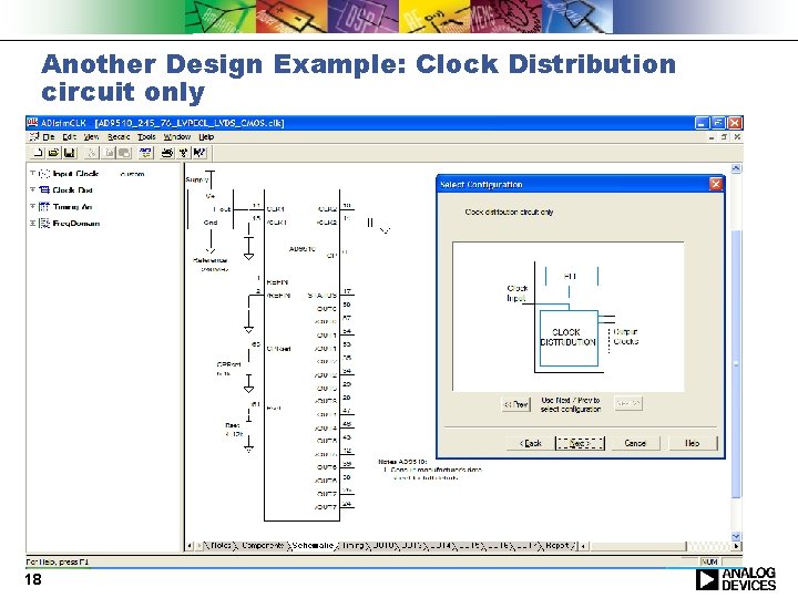
Another Design Example: Clock Distribution circuit only 18

ADIsim. CLK versus Lab measurements 19

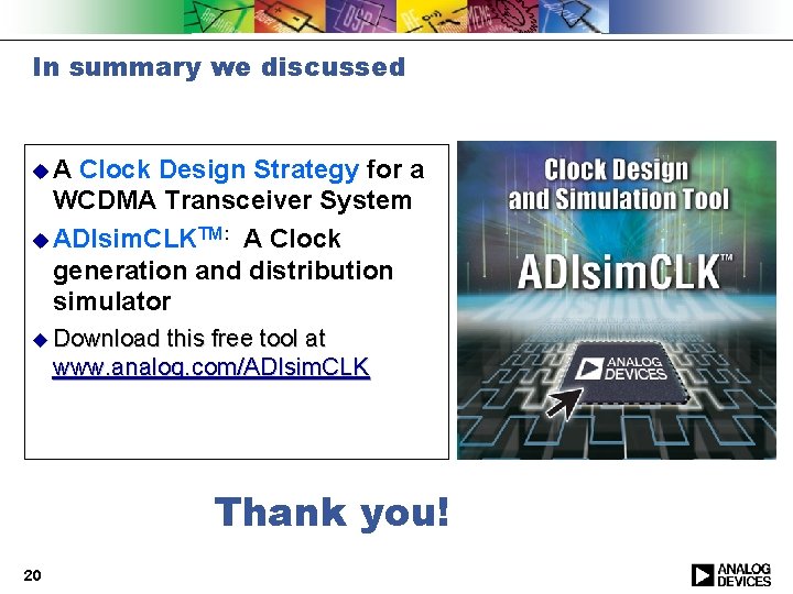
In summary we discussed u. A Clock Design Strategy for a WCDMA Transceiver System u ADIsim. CLKTM: A Clock generation and distribution simulator u Download this free tool at www. analog. com/ADIsim. CLK Thank you! 20

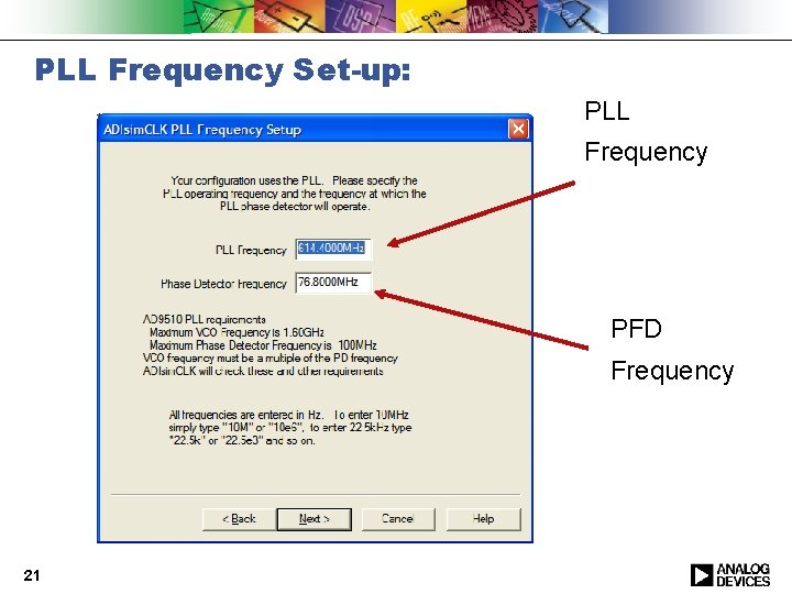
PLL Frequency Set-up: PLL Frequency PFD Frequency 21

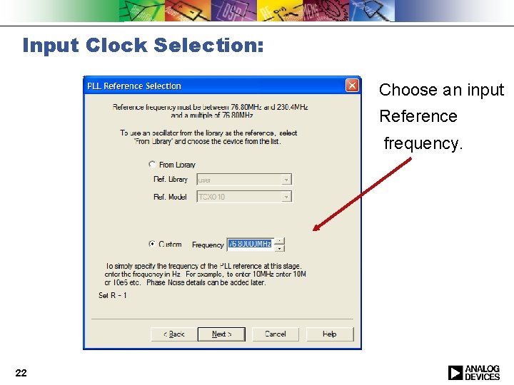
Input Clock Selection: Choose an input Reference frequency. 22

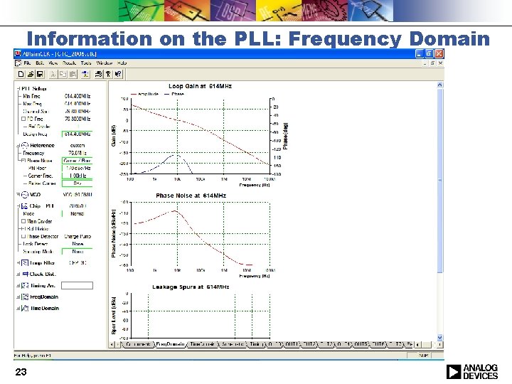
Information on the PLL: Frequency Domain 23

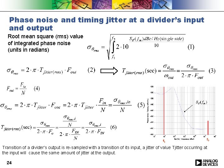
Phase noise and timing jitter at a divider’s input and output Root mean square (rms) value of integrated phase noise (units in radians) Transition of a divider’s output is re-sampled with a transition of its input, a jitter of value Tjitter occurring at the input will cause the same amount of jitter at the output. 24

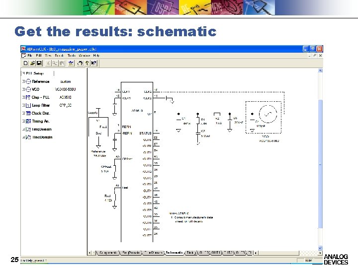
Get the results: schematic 25

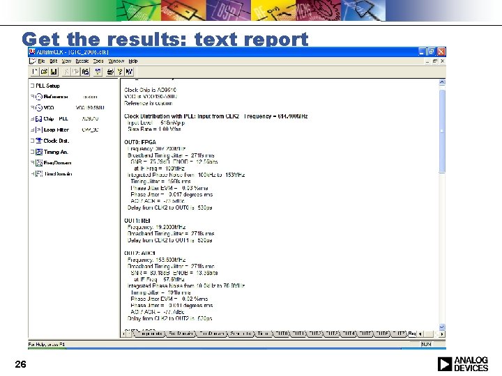
Get the results: text report 26

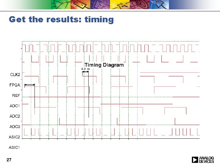
Get the results: timing 0. 11 ns 27