The PSEC3 PSEC4 ASICs 5 15 GSas waveform

- Slides: 32

The PSEC-3 & PSEC-4 ASICs 5 -15 GSa/s waveform sampling/digitizing ICs Eric Oberla 20 -May-2011 LAPPD Electronics + Integration GPC Review

Outline • PSEC series architecture review • PSEC-3 --- testing results – Submitted 11 -Aug-2010, 40 parts received 16 -Dec-2010 • PSEC-4 --- design & specifications – Submitted 9 -May to MOSIS prototyping run • Plans 5/20/2011 LAPPD Electronics + Integration GPC review 2

PSEC series architecture • Waveform sampling using Switched Capacitor Array (SCA) • On-chip digitization up to 12 bits • Serial data readout • Region of interest readout capability • Self-triggering option • Designed to handle fast pulses (MCPs) • • Sampling rate capability > 10 GSa/s Analog bandwidth > 1 GHz (challenge!) Relatively short buffer size Medium event-rate capability (~100 KHz) • IBM 130 nm CMOS process Primary front-end chip for LAPPD MCPs 5/20/2011 LAPPD Electronics + Integration GPC review 3

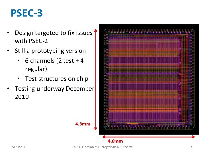
PSEC-3 • Design targeted to fix issues with PSEC-2 • Still a prototyping version • 6 channels (2 test + 4 regular) • Test structures on chip • Testing underway December, 2010 4. 3 mm 4. 0 mm 5/20/2011 LAPPD Electronics + Integration GPC review 4

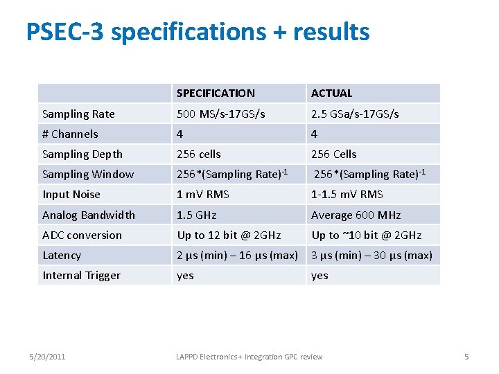
PSEC-3 specifications + results SPECIFICATION ACTUAL Sampling Rate 500 MS/s-17 GS/s 2. 5 GSa/s-17 GS/s # Channels 4 4 Sampling Depth 256 cells 256 Cells Sampling Window 256*(Sampling Rate)-1 Input Noise 1 m. V RMS 1 -1. 5 m. V RMS Analog Bandwidth 1. 5 GHz Average 600 MHz ADC conversion Up to 12 bit @ 2 GHz Up to ~10 bit @ 2 GHz Latency 2 µs (min) – 16 µs (max) 3 µs (min) – 30 µs (max) Internal Trigger yes 5/20/2011 LAPPD Electronics + Integration GPC review 5

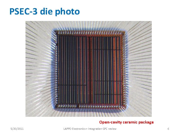
PSEC-3 die photo Open-cavity ceramic package 5/20/2011 LAPPD Electronics + Integration GPC review 6

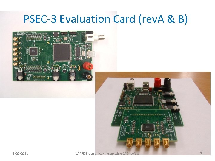
PSEC-3 Evaluation Card (rev. A & B) 5/20/2011 LAPPD Electronics + Integration GPC review 7

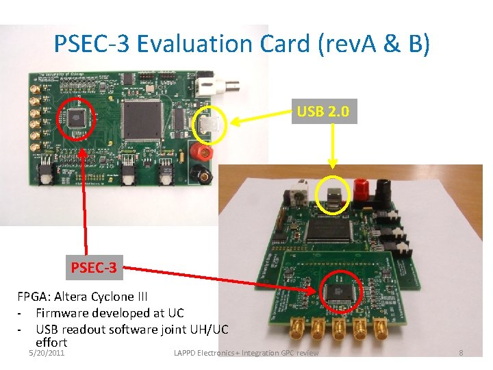
PSEC-3 Evaluation Card (rev. A & B) USB 2. 0 PSEC-3 FPGA: Altera Cyclone III - Firmware developed at UC - USB readout software joint UH/UC effort 5/20/2011 LAPPD Electronics + Integration GPC review 8

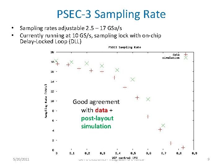
PSEC-3 Sampling Rate • Sampling rates adjustable 2. 5 – 17 GSa/s • Currently running at 10 GS/s, sampling lock with on-chip Delay-Locked Loop (DLL) Good agreement with data + post-layout simulation 5/20/2011 LAPPD Electronics + Integration GPC review 9

PSEC-3 Sample Lock • Custom delay locked loop (DLL) design • Works great, except for some issues of de-locking when ADC is running – Attributed to drop in rail voltage/digital noise ---> issues addressed in PSEC-4 • Video: 5/20/2011 LAPPD Electronics + Integration GPC review 10

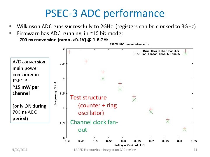
PSEC-3 ADC performance • Wilkinson ADC runs successfully to 2 GHz (registers can be clocked to 3 GHz) • Firmware has ADC running in ~10 bit mode: 700 ns conversion (ramp ->0 -1 V) @ 1. 6 GHz A/D conversion main power consumer in PSEC-3 – ~15 m. W per channel (only ON during 700 ns ADC period) 5/20/2011 Test structure (counter + ring oscillator) Channel clock fanout LAPPD Electronics + Integration GPC review 11

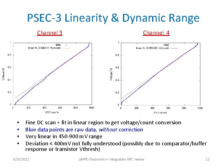
PSEC-3 Linearity & Dynamic Range Channel 3 • • Channel 4 Fine DC scan + fit in linear region to get voltage/count conversion Blue data points are raw data, without correction Very linear in 450 -900 m. V range Deviation < 400 m. V not fully understood (possibly due to comparator/buffer response or transistor Vthresh) 5/20/2011 LAPPD Electronics + Integration GPC review 12

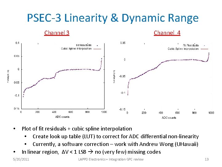
PSEC-3 Linearity & Dynamic Range Channel 3 • • Channel 4 Plot of fit residuals + cubic spline interpolation • Create look up table (LUT) to correct for ADC differential non-linearity • Currently, a software correction – work with Andrew Wong (UHawaii) In linear region, ΔV < 1 LSB no (very few) missing codes 5/20/2011 LAPPD Electronics + Integration GPC review 13

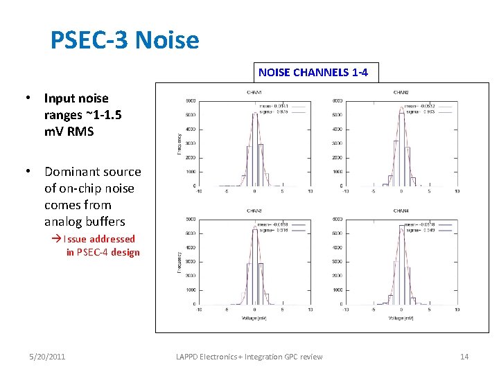
PSEC-3 Noise NOISE CHANNELS 1 -4 • Input noise ranges ~1 -1. 5 m. V RMS • Dominant source of on-chip noise comes from analog buffers Issue addressed in PSEC-4 design 5/20/2011 LAPPD Electronics + Integration GPC review 14

PSEC-3 Noise <noise plots PSEC-3 simulation to compare> 5/20/2011 LAPPD Electronics + Integration GPC review 15

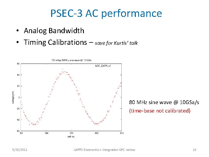
PSEC-3 AC performance • Analog Bandwidth • Timing Calibrations – save for Kurtis’ talk 80 MHz sine wave @ 10 GSa/s (time-base not calibrated) 5/20/2011 LAPPD Electronics + Integration GPC review 16

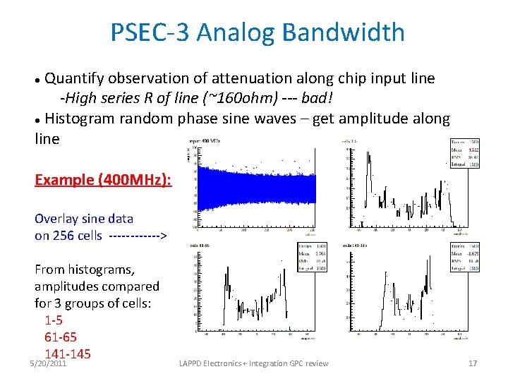
PSEC-3 Analog Bandwidth Quantify observation of attenuation along chip input line -High series R of line (~160 ohm) --- bad! Histogram random phase sine waves – get amplitude along line Example (400 MHz): Overlay sine data on 256 cells ------> From histograms, amplitudes compared for 3 groups of cells: 1 -5 61 -65 141 -145 5/20/2011 LAPPD Electronics + Integration GPC review 17

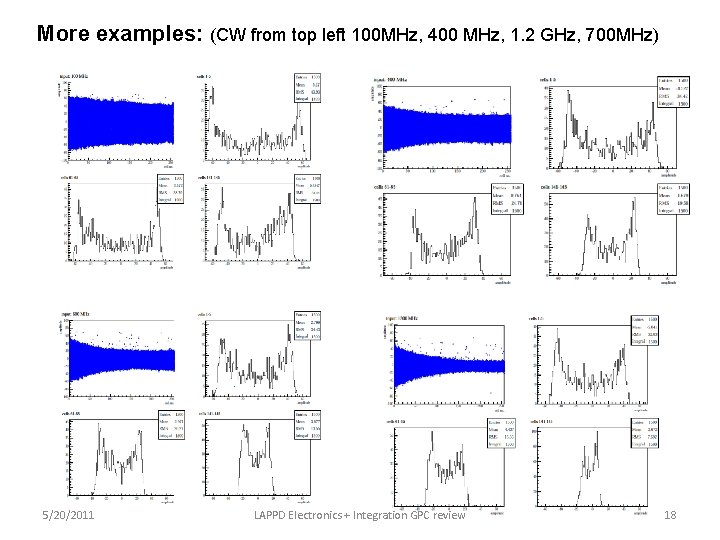
More examples: (CW from top left 100 MHz, 400 MHz, 1. 2 GHz, 700 MHz) 5/20/2011 LAPPD Electronics + Integration GPC review 18

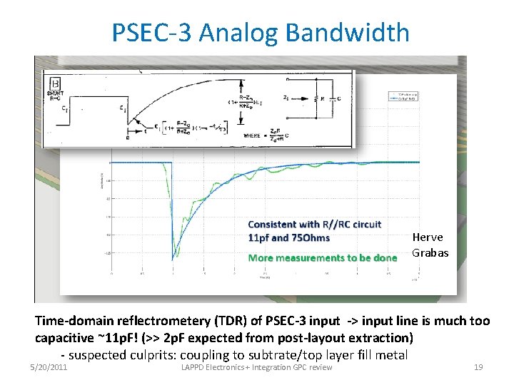
PSEC-3 Analog Bandwidth Herve Grabas Time-domain reflectrometery (TDR) of PSEC-3 input -> input line is much too capacitive ~11 p. F! (>> 2 p. F expected from post-layout extraction) - suspected culprits: coupling to subtrate/top layer fill metal 5/20/2011 LAPPD Electronics + Integration GPC review 19

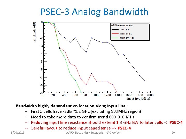
PSEC-3 Analog Bandwidth highly dependent on location along input line: – First 5 cells have -3 d. B ~1. 3 GHz (excluding 800 MHz region) – Need to take more data to confirm trend 600 -900 MHz – Reducing input line resistance should extend 1. 3 GHz BW to later cells –> PSEC-4 -- Careful layout to reduce input capacitance –> PSEC-4 5/20/2011 LAPPD Electronics + Integration GPC review 20

PSEC-3 summary PSEC-3 = working waveform sampling ASIC • Room for improvement: • ABW • Dynamic flip-flops proven difficult in ADC design • Overall readout speed Fixes covered in careful redesign -> PSEC-4 • Still to characterize: • Timing calibrations -> timing measurements (resolution, jitter, etc. ) • Temperature dependence • Up next: Readout a detector! 5/20/2011 LAPPD Electronics + Integration GPC review 21

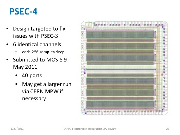
PSEC-4 • Design targeted to fix issues with PSEC-3 • 6 identical channels • each 256 samples deep • Submitted to MOSIS 9 May 2011 • 40 parts • May get a larger run via CERN MPW if necessary 5/20/2011 LAPPD Electronics + Integration GPC review 22

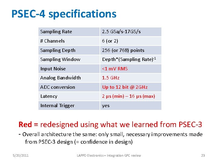
PSEC-4 specifications Sampling Rate 2. 5 GSa/s-17 GS/s # Channels 6 (or 2) Sampling Depth 256 (or 768) points Sampling Window Depth*(Sampling Rate)-1 Input Noise <1 m. V RMS Analog Bandwidth 1. 5 GHz ADC conversion Up to 12 bit @ 2 GHz Latency 2 µs (min) – 16 µs (max) Internal Trigger yes Red = redesigned using what we learned from PSEC-3 - Overall architecture the same: only small, necessary improvements made from PSEC-3 design (= confidence in design) 5/20/2011 LAPPD Electronics + Integration GPC review 23

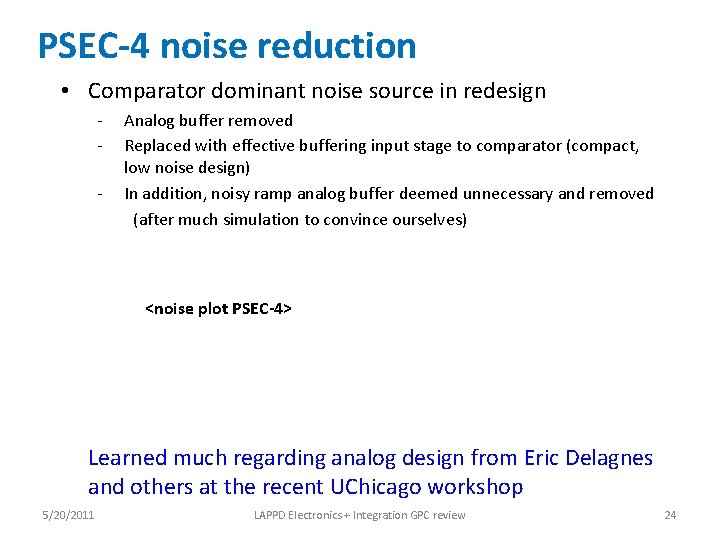
PSEC-4 noise reduction • Comparator dominant noise source in redesign - Analog buffer removed Replaced with effective buffering input stage to comparator (compact, low noise design) In addition, noisy ramp analog buffer deemed unnecessary and removed (after much simulation to convince ourselves) <noise plot PSEC-4> Learned much regarding analog design from Eric Delagnes and others at the recent UChicago workshop 5/20/2011 LAPPD Electronics + Integration GPC review 24

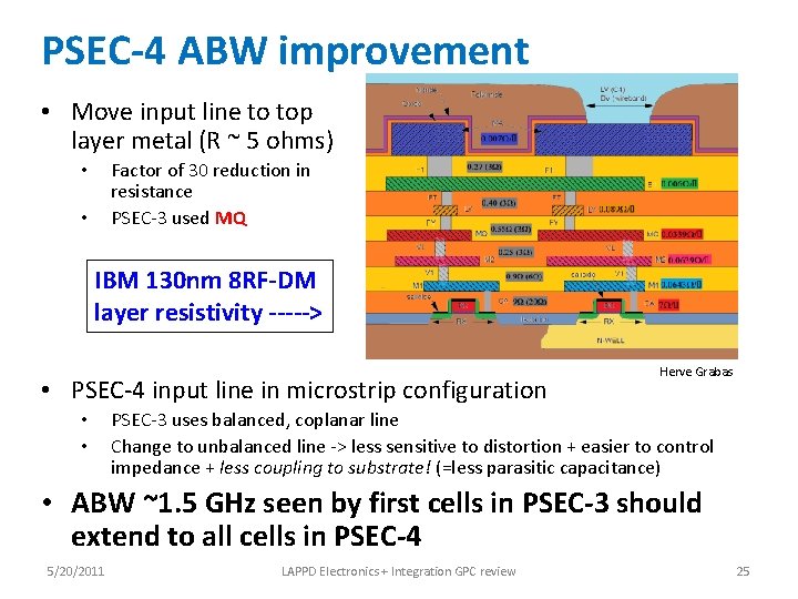
PSEC-4 ABW improvement • Move input line to top layer metal (R ~ 5 ohms) Factor of 30 reduction in resistance PSEC-3 used MQ • • IBM 130 nm 8 RF-DM layer resistivity -----> • PSEC-4 input line in microstrip configuration • • Herve Grabas PSEC-3 uses balanced, coplanar line Change to unbalanced line -> less sensitive to distortion + easier to control impedance + less coupling to substrate! (=less parasitic capacitance) • ABW ~1. 5 GHz seen by first cells in PSEC-3 should extend to all cells in PSEC-4 5/20/2011 LAPPD Electronics + Integration GPC review 25

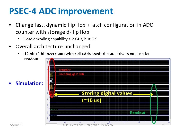
PSEC-4 ADC improvement • Change fast, dynamic flip flop + latch configuration in ADC counter with storage d-flip flop • Lose encoding capability > 2 GHz, but OK • Overall architecture unchanged • 12 bit +1 bit overcount with cell-addressed tri-state drivers on each for readout. Transfer Encoding @ 2 GHz • Simulation: Storing digital values (~10 us) Readout 5/20/2011 LAPPD Electronics + Integration GPC review 26

PSEC-3 & PSEC-4 plans • Parallel work on both chips • PSEC-3: • • • Continue characterizing PSEC-3 – work with Kurtis on time calibrations Timing measurements! Detector readout (later talk for details/opportunities) • PSEC-4: • • • Design of evaluation board (possibly using existing rev. A digital card) Much of PSEC-3 firmware will transfer Characterization (expect chip ~August) • PSEC-4 is baseline ASIC for LAPPD readout. • PSEC-3 is working 4 -channel prototype and will be used extensively in meantime 5/20/2011 LAPPD Electronics + Integration GPC review 27

BACKUP 5/20/2011 LAPPD Electronics + Integration GPC review 28

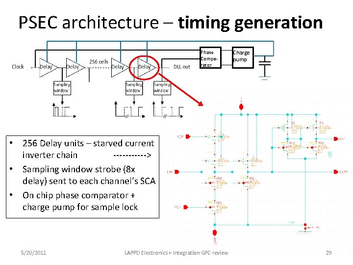
PSEC architecture – timing generation Phase Comparator Charge pump • 256 Delay units – starved current inverter chain ------> • Sampling window strobe (8 x delay) sent to each channel’s SCA • On chip phase comparator + charge pump for sample lock 5/20/2011 LAPPD Electronics + Integration GPC review 29

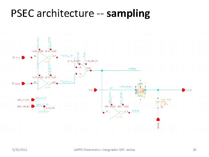
PSEC architecture -- sampling 5/20/2011 LAPPD Electronics + Integration GPC review 30

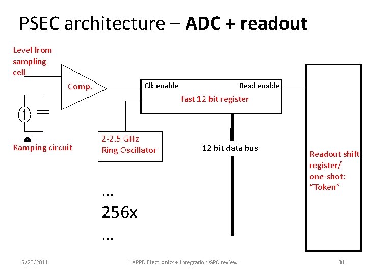
PSEC architecture – ADC + readout Level from sampling cell Comp. Clk enable Read enable fast 12 bit register Ramping circuit 2 -2. 5 GHz Ring Oscillator 12 bit data bus … 256 x … 5/20/2011 LAPPD Electronics + Integration GPC review Readout shift register/ one-shot: “Token” 31

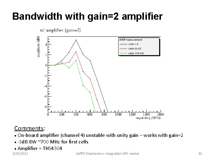
Bandwidth with gain=2 amplifier Comments: On-board amplifier (channel 4) unstable with unity gain – works with gain=2 -3 d. B BW ~700 MHz for first cells Amplifier = THS 4304 5/20/2011 LAPPD Electronics + Integration GPC review 32