The George Washington University School of Engineering and



- Slides: 20

The George Washington University School of Engineering and Applied Science Department of Electrical and Computer Engineering ECE 122 – Lab 5 Latches & Flip-flops Jason Woytowich Ritu Bajpai Last revised on October 15, 2007

What are Latches & Flip-flops? • They are single bit memory elements • Latches change state whenever the inputs dictate it • Flip-flops only change state on rising or falling clock edges

Lab Activities • Build and test an SR Latch from NAND Gates. • Build and test a D Latch from the SR Latch • Build and test a DFF from your D Latch: – Master Slave implementation (MS) – Positive gate trigger implementation (PGT) • We will do only schematic simulation in today's lab and will test our circuit for all possible combinations of input.

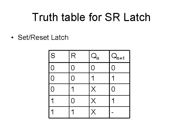
Truth table for SR Latch • Set/Reset Latch S R Qn Qn+1 0 0 0 1 0 1 X 0 1 0 X 1 1 1 X -

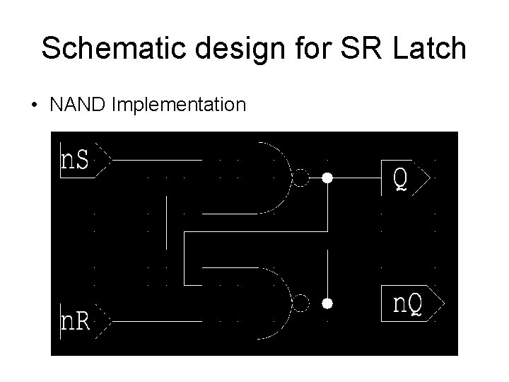
Schematic design for SR Latch • NAND Implementation

Can you make a schematic design for a SR NOR latch? • Start from NAND latch. • Show step by step procedure to replace NAND gates by NOR gates. • Do the inputs/outputs remain the same for NAND and NOR latch?

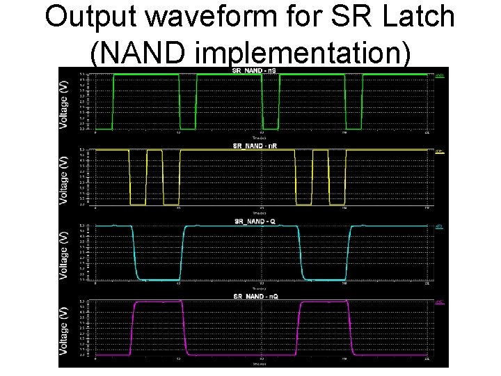
Output waveform for SR Latch (NAND implementation)

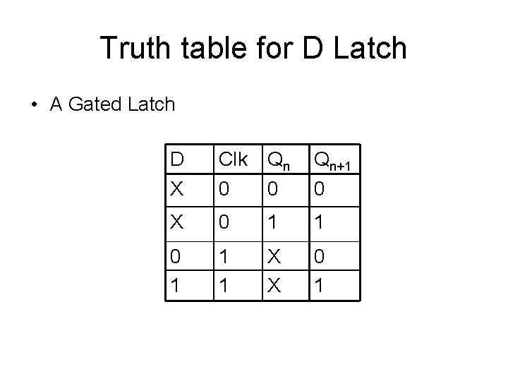
Truth table for D Latch • A Gated Latch D X Clk 0 Qn+1 0 X 0 1 1 1 X X 0 1

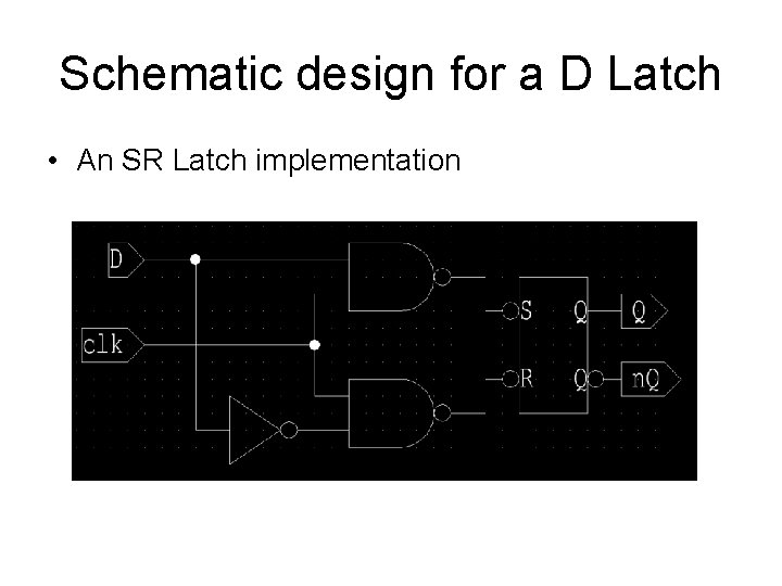
Schematic design for a D Latch • An SR Latch implementation

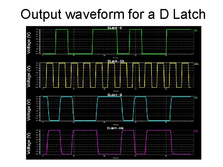
Output waveform for a D Latch

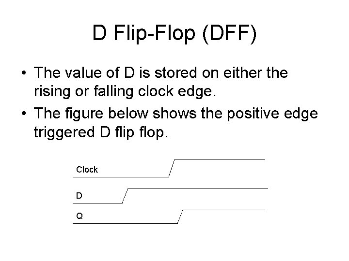
D Flip-Flop (DFF) • The value of D is stored on either the rising or falling clock edge. • The figure below shows the positive edge triggered D flip flop. Clock D Q

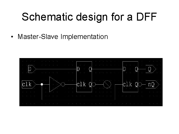
Schematic design for a DFF • Master-Slave Implementation

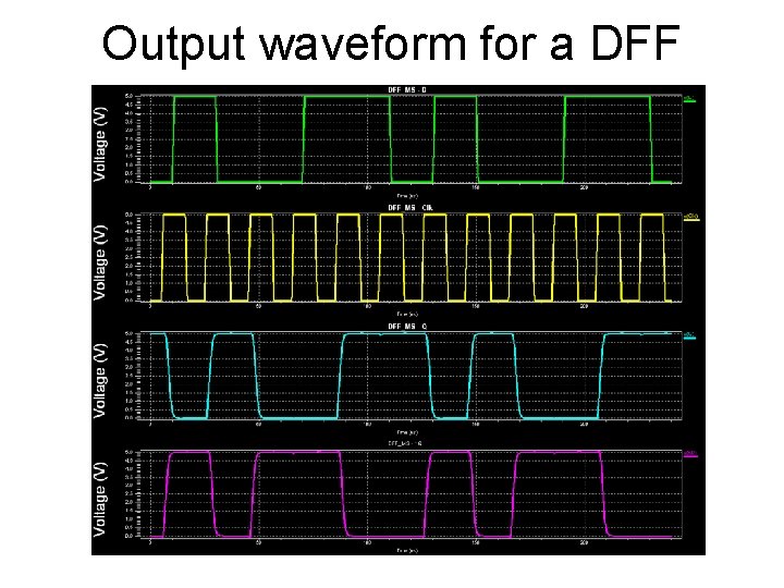
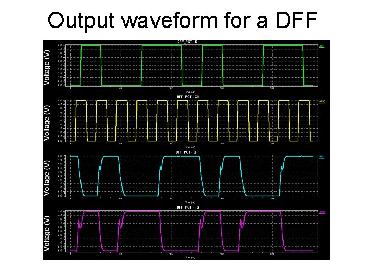
Output waveform for a DFF

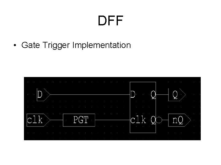
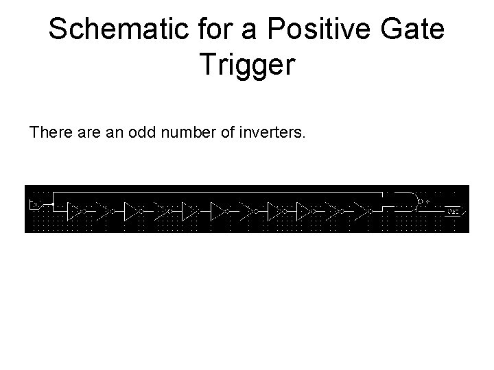
DFF • Gate Trigger Implementation

Schematic for a Positive Gate Trigger There an odd number of inverters.

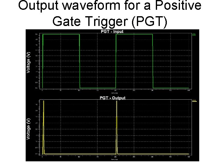
Output waveform for a Positive Gate Trigger (PGT)

Can you explain the output waveform of the PGT? • Why do we use an odd number of inverters to make a PGT? • Could we have used even number of inverters and replaced the AND gate by NOR, NAND or OR gate to obtain a similar output?

Output waveform for a DFF

Results • Give clear output waveforms for all the circuits that you implemented in today’s lab. • Ensure that our output waveforms show that you have covered all the test cases.

Analysis • So far you have seen that you obtain glitches or peaks in your output during transition of input from one state to another. After doing this lab can you suggest a way to get rid of those glitches and peaks? • Keeping the above question in mind can you state one probable use of D flip flops in digital circuits?