The ATLAS Pixel Detector Introduction Outline The Pixel
- Slides: 24

The ATLAS Pixel Detector - Introduction -

Outline § The Pixel Detector – – – General The Pixel Module The FE Chips MCC and Optolink Off-Detector Hardware § Standard Operating Conditions § Caveats § Basic Calibrations ATLAS Pixel Detector - Introduction 2

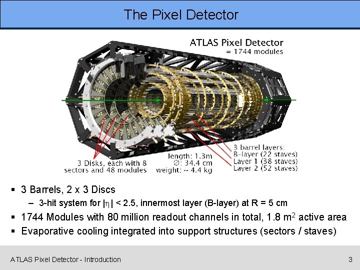
The Pixel Detector § 3 Barrels, 2 x 3 Discs – 3 -hit system for |h| < 2. 5, innermost layer (B-layer) at R = 5 cm § 1744 Modules with 80 million readout channels in total, 1. 8 m 2 active area § Evaporative cooling integrated into support structures (sectors / staves) ATLAS Pixel Detector - Introduction 3

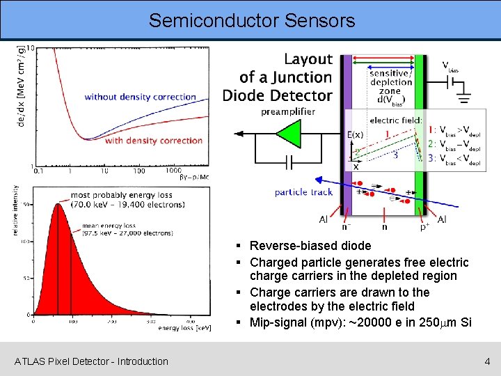
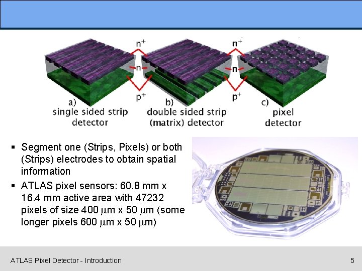
Semiconductor Sensors § Reverse-biased diode § Charged particle generates free electric charge carriers in the depleted region § Charge carriers are drawn to the electrodes by the electric field § Mip-signal (mpv): ~20000 e in 250 mm Si ATLAS Pixel Detector - Introduction 4

§ Segment one (Strips, Pixels) or both (Strips) electrodes to obtain spatial information § ATLAS pixel sensors: 60. 8 mm x 16. 4 mm active area with 47232 pixels of size 400 mm x 50 mm (some longer pixels 600 mm x 50 mm) ATLAS Pixel Detector - Introduction 5

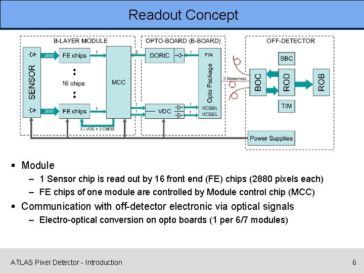
Readout Concept § Module – 1 Sensor chip is read out by 16 front end (FE) chips (2880 pixels each) – FE chips of one module are controlled by Module control chip (MCC) § Communication with off-detector electronic via optical signals – Electro-optical conversion on opto boards (1 per 6/7 modules) ATLAS Pixel Detector - Introduction 6

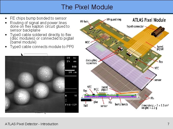
The Pixel Module § FE chips bump bonded to sensor § Routing of signal and power lines done on flex kapton circuit glued to sensor backplane § Type 0 cable soldered directly to flex (disc modules) or connected to pigtail (barrel module) § Type 0 cable connects module to PP 0 ATLAS Pixel Detector - Introduction 7

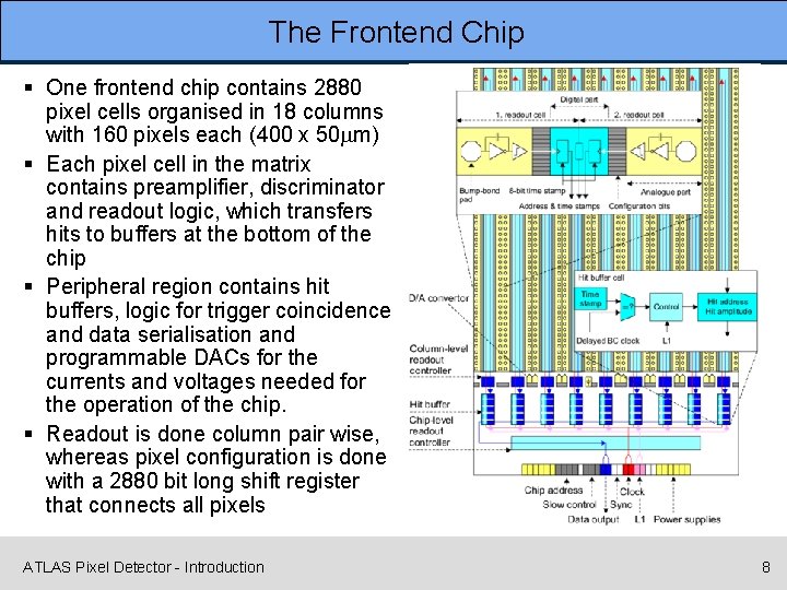
The Frontend Chip § One frontend chip contains 2880 pixel cells organised in 18 columns with 160 pixels each (400 x 50 mm) § Each pixel cell in the matrix contains preamplifier, discriminator and readout logic, which transfers hits to buffers at the bottom of the chip § Peripheral region contains hit buffers, logic for trigger coincidence and data serialisation and programmable DACs for the currents and voltages needed for the operation of the chip. § Readout is done column pair wise, whereas pixel configuration is done with a 2880 bit long shift register that connects all pixels ATLAS Pixel Detector - Introduction 8

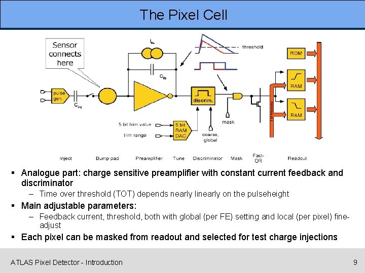
The Pixel Cell § Analogue part: charge sensitive preamplifier with constant current feedback and discriminator – Time over threshold (TOT) depends nearly linearly on the pulseheight § Main adjustable parameters: – Feedback current, threshold, both with global (per FE) setting and local (per pixel) fineadjust § Each pixel can be masked from readout and selected for test charge injections ATLAS Pixel Detector - Introduction 9

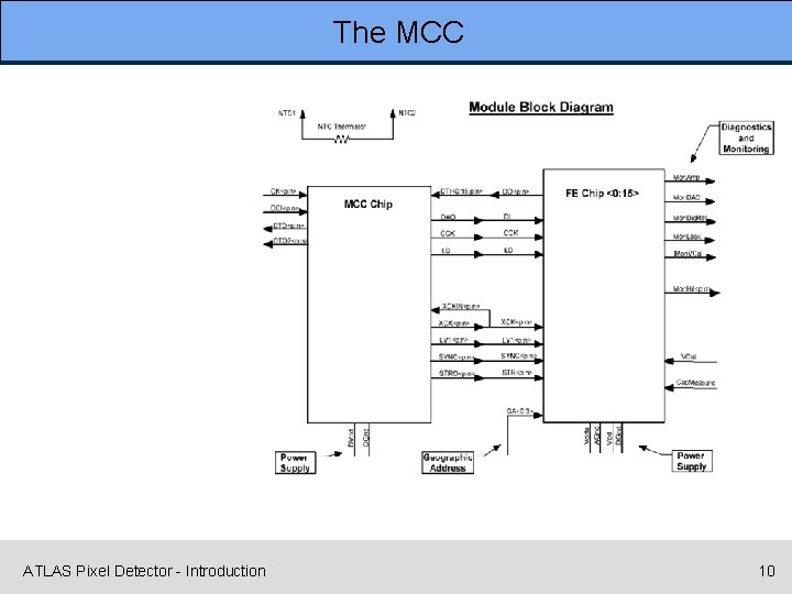
The MCC ATLAS Pixel Detector - Introduction 10

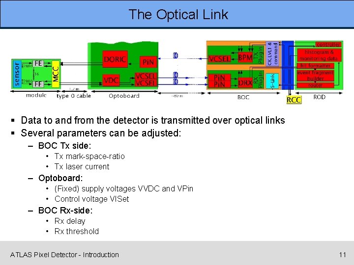
The Optical Link § Data to and from the detector is transmitted over optical links § Several parameters can be adjusted: – BOC Tx side: • Tx mark-space-ratio • Tx laser current – Optoboard: • (Fixed) supply voltages VVDC and VPin • Control voltage VISet – BOC Rx-side: • Rx delay • Rx threshold ATLAS Pixel Detector - Introduction 11

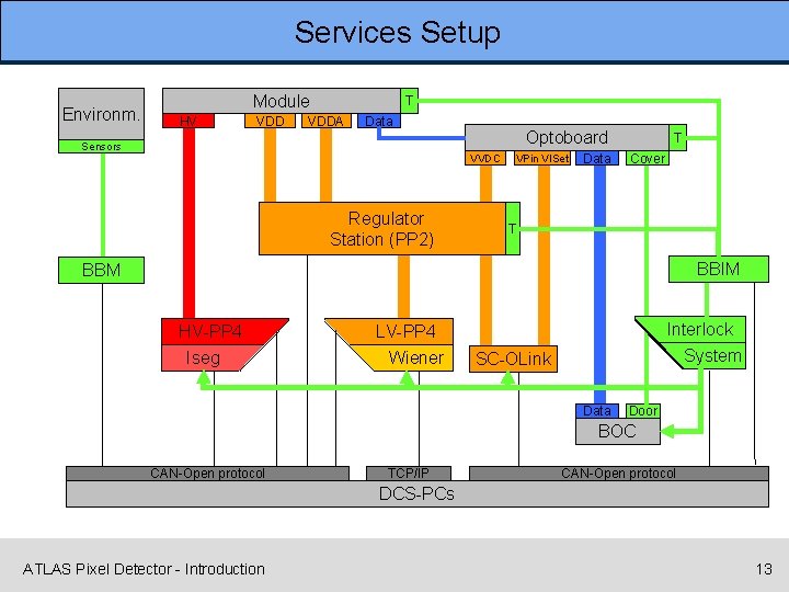
Services Requirements § Each module: – – 1 sensor bias voltage (now 150 V, higher after irradiation) 1 digital voltage (2. 0 – 2. 1 V) for FE chips and MCC 1 analogue voltage (1. 6 – 1. 7 V) for FE chips 1 NTC connection § Each optoboard (1 per 6/7 modules): – 1 “high-current” (250 m. A) voltage for the VCSEL driver chip (needs regulation) – Several low-current voltages (not regulated): • Bias voltage VPin for pin diode • Control voltage VISet to regulate light output of on-detector lasers • Reset signal – 1 NTC connection ATLAS Pixel Detector - Introduction 12

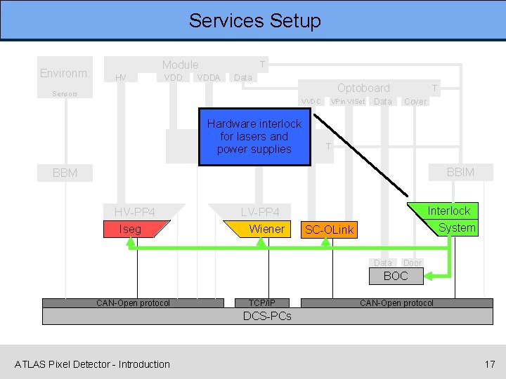
Services Setup Environm. Module HV VDD T VDDA Data Sensors Optoboard VVDC Regulator Station (PP 2) VPin VISet Data T Cover T BBIM BBM HV-PP 4 Iseg LV-PP 4 Wiener Interlock System SC-OLink Data Door BOC CAN-Open protocol TCP/IP CAN-Open protocol DCS-PCs ATLAS Pixel Detector - Introduction 13

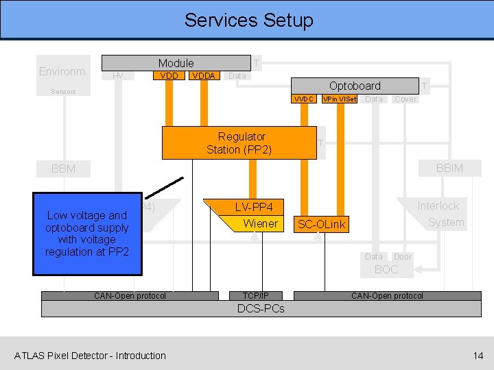
Services Setup Environm. Module HV VDD T VDDA Data Sensors Optoboard VVDC Regulator Station (PP 2) VPin VISet Data T Cover T BBIM BBM (HV-PP 4) Low voltage and Iseg optoboard supply with voltage regulation at PP 2 LV-PP 4 Wiener Interlock System SC-OLink Data Door BOC CAN-Open protocol TCP/IP CAN-Open protocol DCS-PCs ATLAS Pixel Detector - Introduction 14

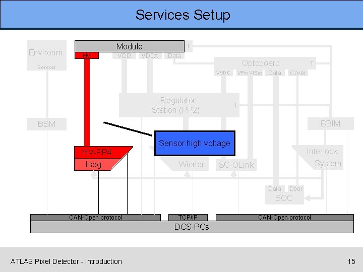
Services Setup Environm. Module HV VDD T VDDA Data Sensors Optoboard VVDC Regulator Station (PP 2) VPin VISet Data T Cover T BBIM BBM HV-PP 4 Iseg Sensor high voltage LV-PP 4 Wiener SC-OLink Interlock System Data Door BOC CAN-Open protocol TCP/IP CAN-Open protocol DCS-PCs ATLAS Pixel Detector - Introduction 15

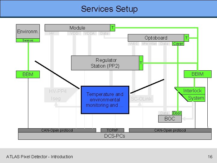
Services Setup Environm. Module HV VDD T VDDA Data Sensors Optoboard VVDC Regulator Station (PP 2) VPin VISet Data T Cover T BBIM BBM HV-PP 4 Iseg LV-PP 4 Temperature and Wiener environmental monitoring and … Interlock System SC-OLink Data Door BOC CAN-Open protocol TCP/IP CAN-Open protocol DCS-PCs ATLAS Pixel Detector - Introduction 16

Services Setup Environm. Module HV VDD T VDDA Data Sensors Optoboard VVDC Hardware interlock for lasers and Regulator power supplies Station VPin VISet Data T Cover T BBIM BBM HV-PP 4 Iseg LV-PP 4 Wiener Interlock System SC-OLink Data Door BOC CAN-Open protocol TCP/IP CAN-Open protocol DCS-PCs ATLAS Pixel Detector - Introduction 17

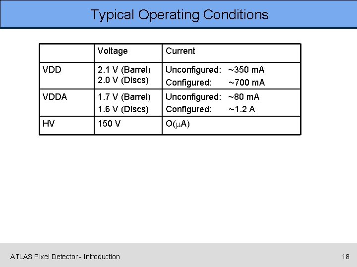
Typical Operating Conditions Voltage Current VDD 2. 1 V (Barrel) 2. 0 V (Discs) Unconfigured: ~350 m. A Configured: ~700 m. A VDDA 1. 7 V (Barrel) 1. 6 V (Discs) Unconfigured: ~80 m. A Configured: ~1. 2 A HV 150 V O(m. A) ATLAS Pixel Detector - Introduction 18

Basic Calibration Measurements § This gives an overview over the most important calibration measurements. § A more complete set of description is available from the pixel detector wiki – https: //twiki. cern. ch/twiki/bin/view/Atlas/Calibration. Description § Or in the calibration document, available on the pixel detector wiki – https: //twiki. cern. ch/twiki/bin/view/Atlas/Pixel. Detector. Group ATLAS Pixel Detector - Introduction 19

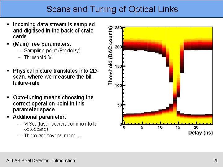
Scans and Tuning of Optical Links § Incoming data stream is sampled and digitised in the back-of-crate cards § (Main) free parameters: – Sampling point (Rx delay) – Threshold 0/1 § Physical picture translates into 2 Dscan, where we measure the bitfailure-rate § Opto-tuning means choosing the correct operation point in this parameter space § Additional parameter: – VISet (laser power, common to full optoboard) – There are several more… ATLAS Pixel Detector - Introduction 20

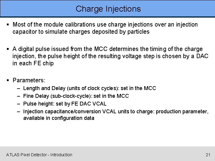
Charge Injections § Most of the module calibrations use charge injections over an injection capacitor to simulate charges deposited by particles § A digital pulse issued from the MCC determines the timing of the charge injection, the pulse height of the resulting voltage step is chosen by a DAC in each FE chip § Parameters: – – Length and Delay (units of clock cycles): set in the MCC Fine Delay (sub-clock-cycle): set in the MCC Pulse height: set by FE DAC VCAL Injection capacitance/conversion VCAL units to charge: production parameter, available in configuration data ATLAS Pixel Detector - Introduction 21

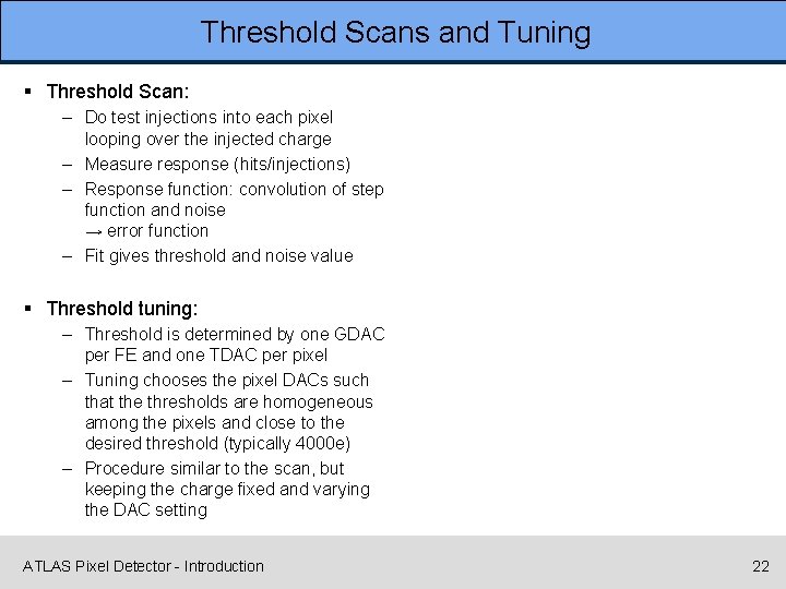
Threshold Scans and Tuning § Threshold Scan: – Do test injections into each pixel looping over the injected charge – Measure response (hits/injections) – Response function: convolution of step function and noise → error function – Fit gives threshold and noise value § Threshold tuning: – Threshold is determined by one GDAC per FE and one TDAC per pixel – Tuning chooses the pixel DACs such that the thresholds are homogeneous among the pixels and close to the desired threshold (typically 4000 e) – Procedure similar to the scan, but keeping the charge fixed and varying the DAC setting ATLAS Pixel Detector - Introduction 22

ATLAS Pixel Detector - Introduction 23

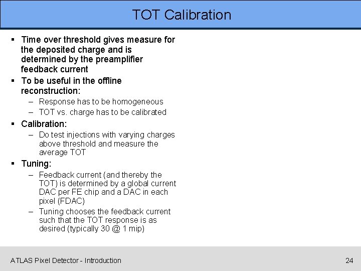
TOT Calibration § Time over threshold gives measure for the deposited charge and is determined by the preamplifier feedback current § To be useful in the offline reconstruction: – Response has to be homogeneous – TOT vs. charge has to be calibrated § Calibration: – Do test injections with varying charges above threshold and measure the average TOT § Tuning: – Feedback current (and thereby the TOT) is determined by a global current DAC per FE chip and a DAC in each pixel (FDAC) – Tuning chooses the feedback current such that the TOT response is as desired (typically 30 @ 1 mip) ATLAS Pixel Detector - Introduction 24