TCT measurements with irradiated strip detectors Igor Mandi1
- Slides: 20

TCT measurements with irradiated strip detectors Igor Mandić1, Vladimir Cindro 1, Andrej Gorišek 1, Gregor Kramberger 1, Marko Milovanović1, Marko Mikuž 1, 2, Marko Zavrtanik 1 1 Jožef 2 Stefan Institute, Ljubljana, Slovenia Faculty of Mathematics and Physics, University of Ljubljana, Slovenia Most measurements made by diploma student Mitja Krnel 1

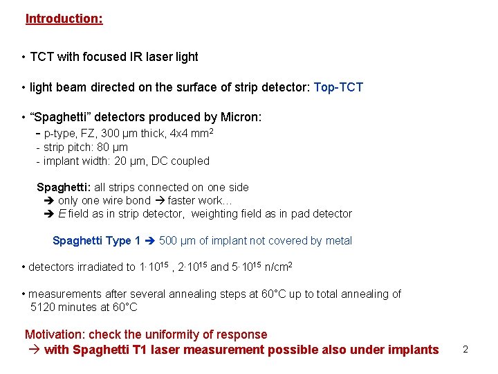
Introduction: • TCT with focused IR laser light • light beam directed on the surface of strip detector: Top-TCT • “Spaghetti” detectors produced by Micron: - p-type, FZ, 300 µm thick, 4 x 4 mm 2 - strip pitch: 80 µm - implant width: 20 µm, DC coupled Spaghetti: all strips connected on one side only one wire bond faster work… E field as in strip detector, weighting field as in pad detector Spaghetti Type 1 500 µm of implant not covered by metal • detectors irradiated to 1∙ 1015 , 2∙ 1015 and 5∙ 1015 n/cm 2 • measurements after several annealing steps at 60°C up to total annealing of 5120 minutes at 60°C Motivation: check the uniformity of response with Spaghetti T 1 laser measurement possible also under implants 2

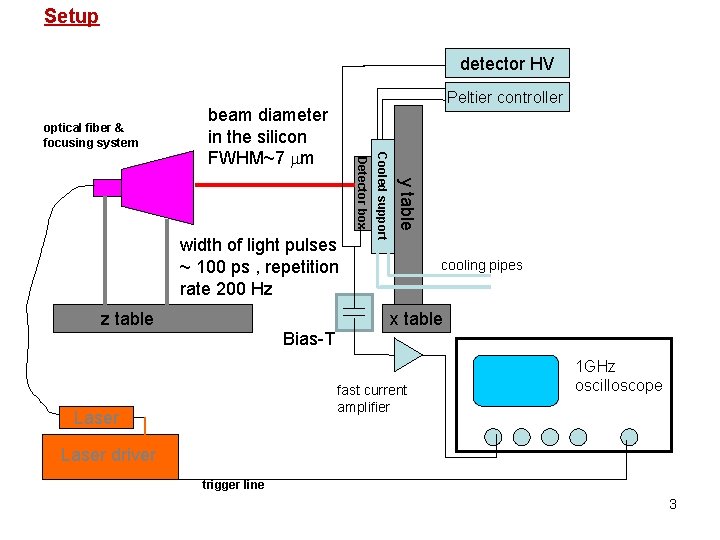
Setup detector HV optical fiber & focusing system Peltier controller z table Bias-T y table width of light pulses ~ 100 ps , repetition rate 200 Hz Cooled support Detector box beam diameter in the silicon FWHM~7 mm cooling pipes x table fast current amplifier Laser 1 GHz oscilloscope Laser driver trigger line 3

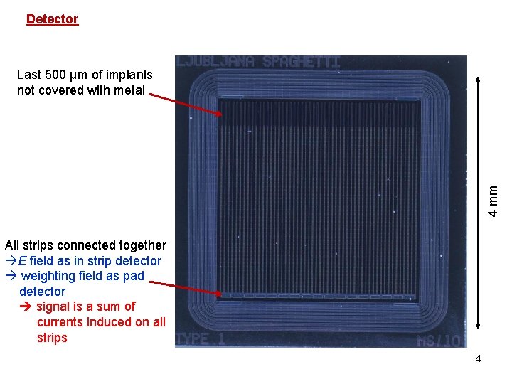
Detector 4 mm Last 500 µm of implants not covered with metal All strips connected together E field as in strip detector weighting field as pad detector signal is a sum of currents induced on all strips 4

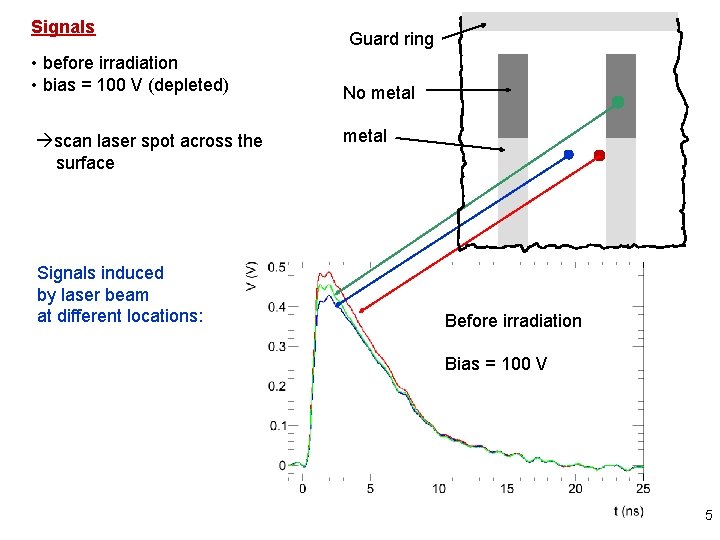
Signals • before irradiation • bias = 100 V (depleted) scan laser spot across the surface Signals induced by laser beam at different locations: Guard ring No metal Before irradiation Bias = 100 V 5

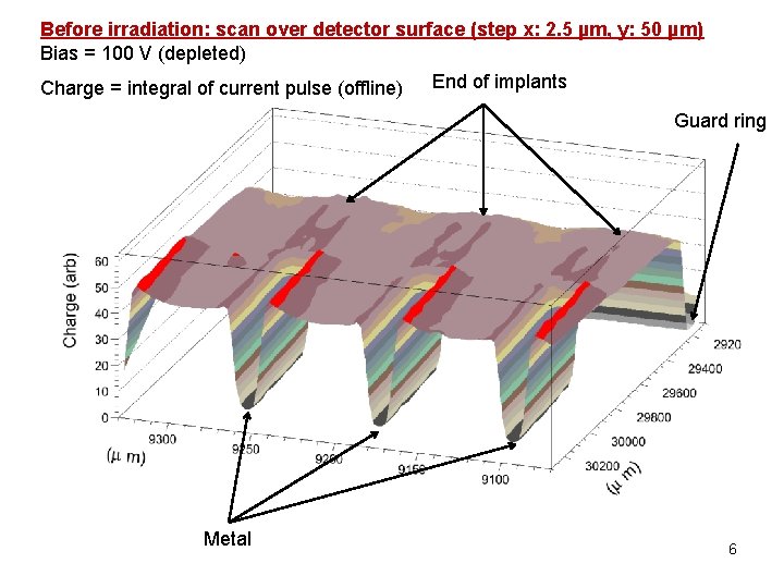
Before irradiation: scan over detector surface (step x: 2. 5 µm, y: 50 µm) Bias = 100 V (depleted) End of implants Charge = integral of current pulse (offline) Guard ring Metal 6

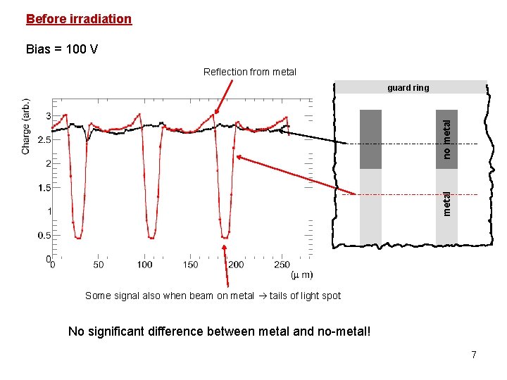
Before irradiation Bias = 100 V Reflection from metal no metal guard ring Some signal also when beam on metal tails of light spot No significant difference between metal and no-metal! 7

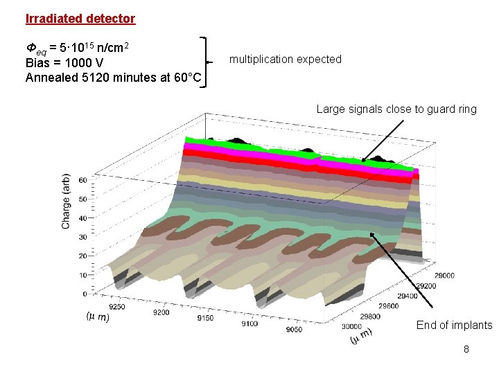
Irradiated detector Φeq = 5· 1015 n/cm 2 Bias = 1000 V Annealed 5120 minutes at 60°C multiplication expected Large signals close to guard ring End of implants 8

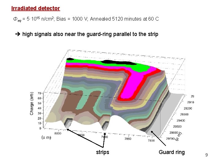
Irradiated detector Φeq = 5· 1015 n/cm 2; Bias = 1000 V; Annealed 5120 minutes at 60 C high signals also near the guard-ring parallel to the strips Guard ring 9

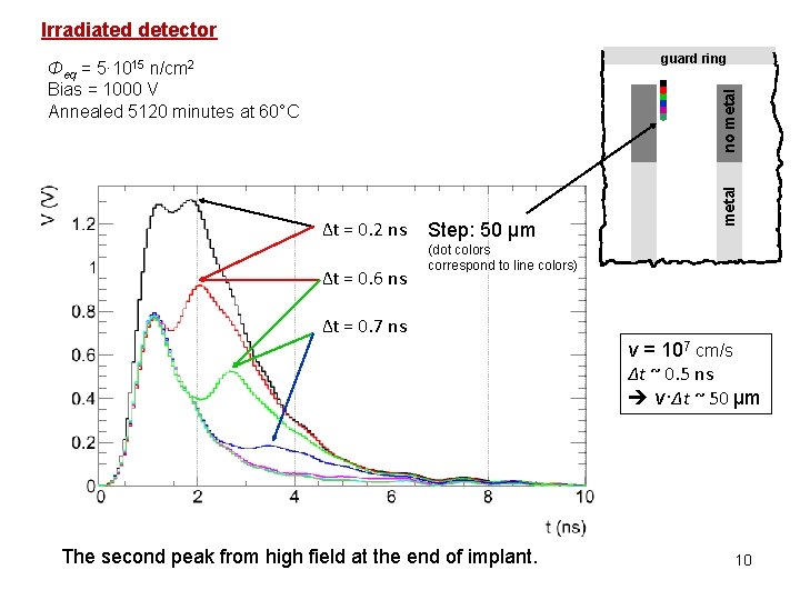
Irradiated detector guard ring Δt = 0. 2 ns Δt = 0. 6 ns Step: 50 µm metal no metal Φeq = 5· 1015 n/cm 2 Bias = 1000 V Annealed 5120 minutes at 60°C (dot colors correspond to line colors) Δt = 0. 7 ns v = 107 cm/s Δt ~ 0. 5 ns v·Δt ~ 50 µm The second peak from high field at the end of implant. 10

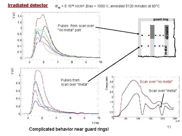
Irradiated detector Φeq = 5· 1015 n/cm 2 , Bias = 1000 V, annealed 5120 minutes at 60°C metal Pulses from scan over “no metal” part no metal guard ring Pulses from scan over “metal” Scan over “no metal” Scan over “metal” Complicated behavior near guard rings! 11

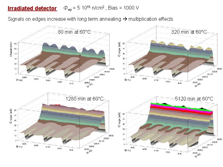
Irradiated detector Φeq = 5· 1015 n/cm 2 , Bias = 1000 V Signals on edges increase with long term annealing multiplication effects 80 min at 60°C 1280 min at 60°C 320 min at 60°C 5120 min at 60°C 12

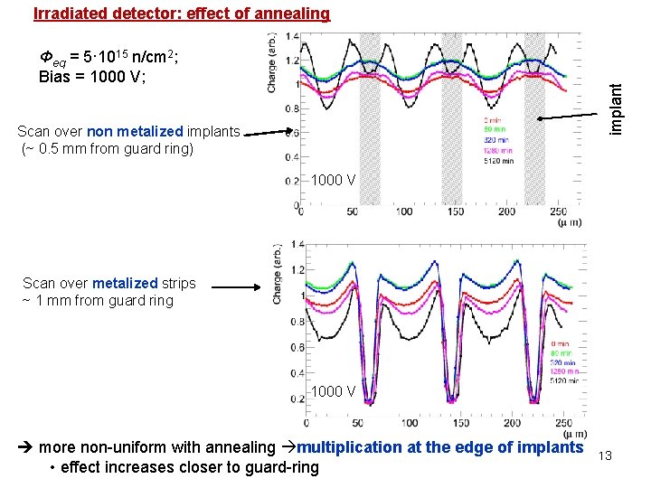
Irradiated detector: effect of annealing implant Φeq = 5· 1015 n/cm 2; Bias = 1000 V; Scan over non metalized implants (~ 0. 5 mm from guard ring) 1000 V Scan over metalized strips ~ 1 mm from guard ring 1000 V more non-uniform with annealing multiplication at the edge of implants • effect increases closer to guard-ring 13

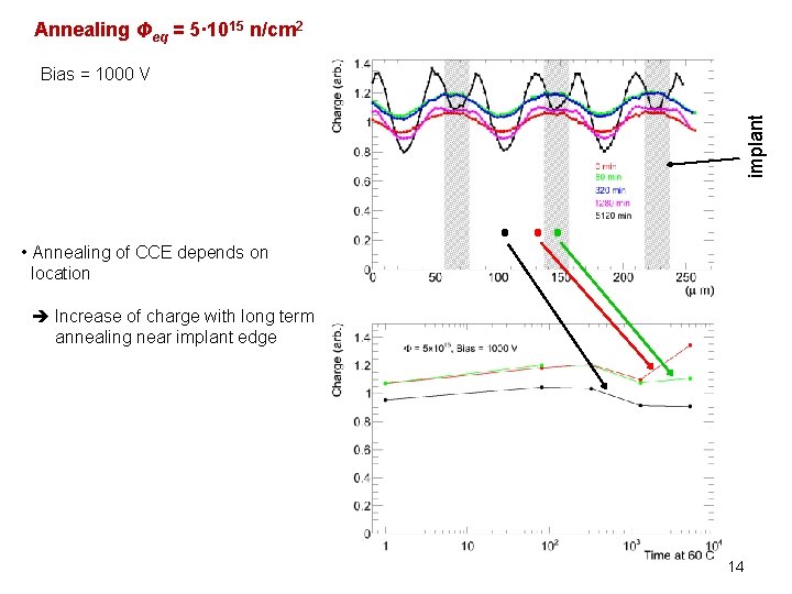
Annealing Φeq = 5· 1015 n/cm 2 implant Bias = 1000 V • Annealing of CCE depends on location Increase of charge with long term annealing near implant edge 14

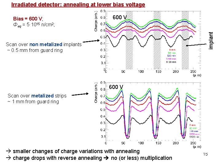
Irradiated detector: annealing at lower bias voltage 600 V implant Bias = 600 V; Φeq = 5· 1015 n/cm 2; Scan over non metalized implants ~ 0. 5 mm from guard ring 600 V Scan over metalized strips ~ 1 mm from guard ring smaller changes of charge variations with annealing charge drops with reverse annealing no (or less) multiplication 15

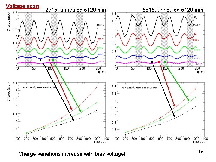
Voltage scan 2 e 15, annealed 5120 min Charge variations increase with bias voltage! 5 e 15, annealed 5120 min 16

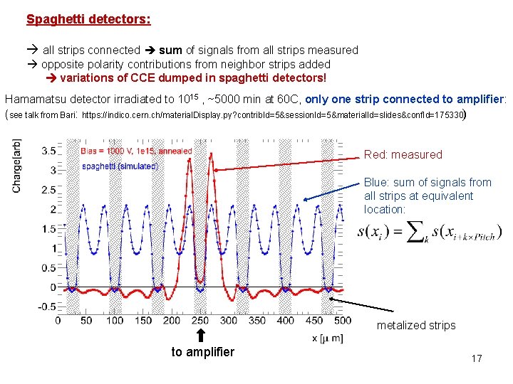
Spaghetti detectors: all strips connected sum of signals from all strips measured opposite polarity contributions from neighbor strips added variations of CCE dumped in spaghetti detectors! Hamamatsu detector irradiated to 1015 , ~5000 min at 60 C, only one strip connected to amplifier: (see talk from Bari: https: //indico. cern. ch/material. Display. py? contrib. Id=5&session. Id=5&material. Id=slides&conf. Id=175330) Red: measured Blue: sum of signals from all strips at equivalent location: metalized strips to amplifier 17

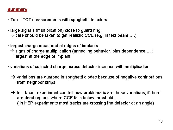
Summary • Top – TCT measurements with spaghetti detectors • large signals (multiplication) close to guard ring care should be taken to get realistic CCE (e. g. in test beam …. ) • largest charge measured at edges of implants signs of charge multiplication (annealing behavior, bias dependence … ) largest at the edge of implant • variations of collected charge across detector increase with multiplication variations are dumped in spaghetti diodes because of negative contributions from neighbor strips test beam experiment can tell how problematic are these variations, if there are dead regions where CCE falls below threshold …. ( in HEP experiments most tracks are crossing the detector at an angle) 18

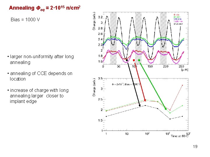
Annealing Φeq = 2· 1015 n/cm 2 Bias = 1000 V • larger non-uniformity after long annealing • annealing of CCE depends on location • increase of charge with long annealing larger closer to implant edge 19

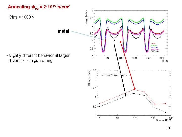
Annealing Φeq = 2· 1015 n/cm 2 Bias = 1000 V metal • slightly different behavior at larger distance from guard-ring 20