Introduction to Sensors and Motors Copier Jam Detector
- Slides: 15

Introduction to Sensors and Motors: Copier Jam Detector DMS-VEX or DLB-VEX Digital Electronics © 2014 Project Lead The Way, Inc.

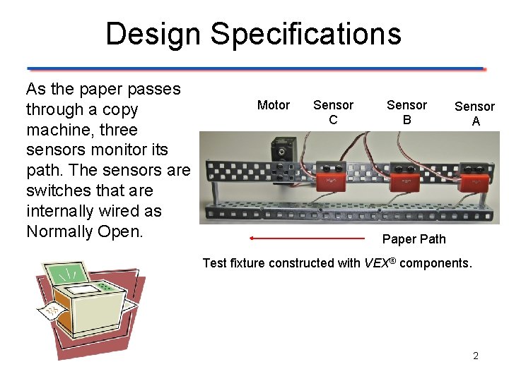
Design Specifications As the paper passes through a copy machine, three sensors monitor its path. The sensors are switches that are internally wired as Normally Open. Motor Sensor C Sensor B Sensor A Paper Path Test fixture constructed with VEX® components. 2

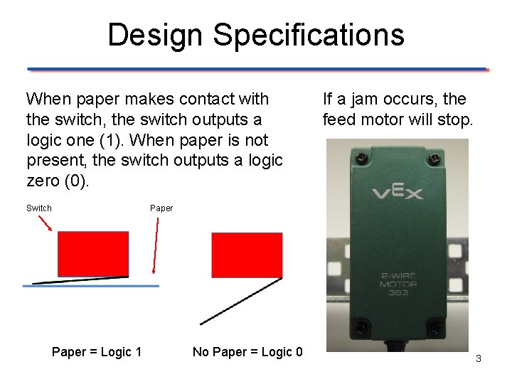
Design Specifications When paper makes contact with the switch, the switch outputs a logic one (1). When paper is not present, the switch outputs a logic zero (0). Switch If a jam occurs, the feed motor will stop. Paper = Logic 1 No Paper = Logic 0 3

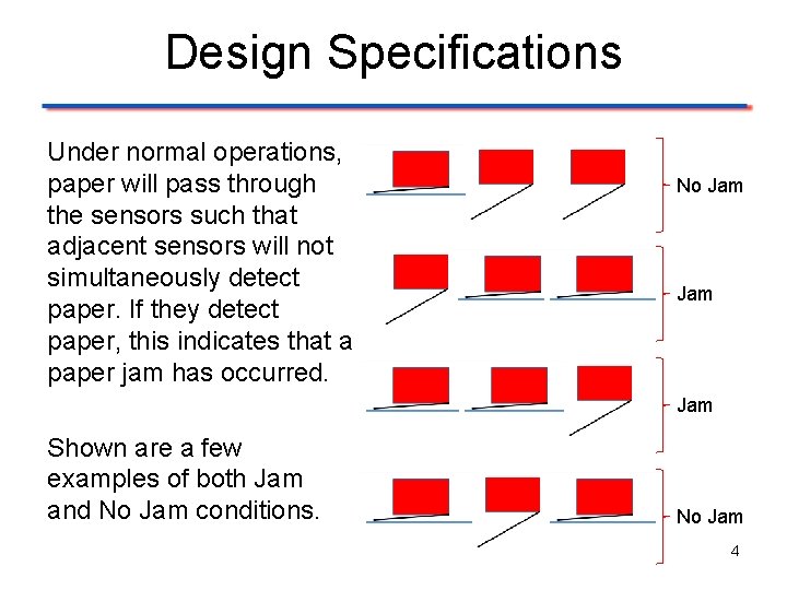
Design Specifications Under normal operations, paper will pass through the sensors such that adjacent sensors will not simultaneously detect paper. If they detect paper, this indicates that a paper jam has occurred. No Jam Jam Shown are a few examples of both Jam and No Jam conditions. No Jam 4

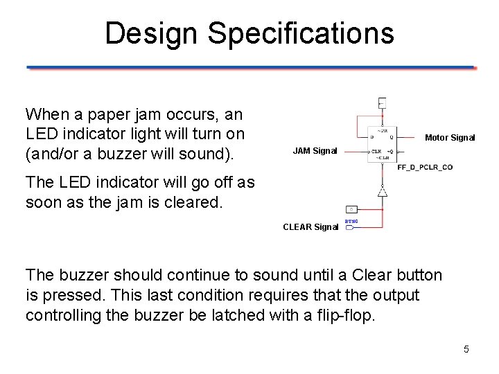
Design Specifications When a paper jam occurs, an LED indicator light will turn on (and/or a buzzer will sound). Motor Signal JAM Signal The LED indicator will go off as soon as the jam is cleared. CLEAR Signal The buzzer should continue to sound until a Clear button is pressed. This last condition requires that the output controlling the buzzer be latched with a flip-flop. 5

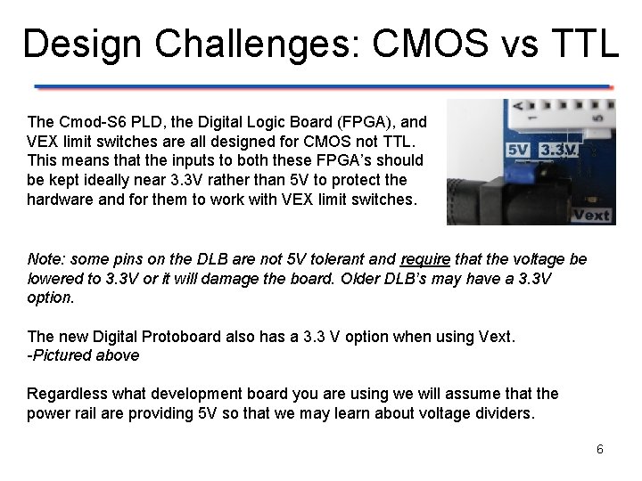
Design Challenges: CMOS vs TTL The Cmod-S 6 PLD, the Digital Logic Board (FPGA), and VEX limit switches are all designed for CMOS not TTL. This means that the inputs to both these FPGA’s should be kept ideally near 3. 3 V rather than 5 V to protect the hardware and for them to work with VEX limit switches. Note: some pins on the DLB are not 5 V tolerant and require that the voltage be lowered to 3. 3 V or it will damage the board. Older DLB’s may have a 3. 3 V option. The new Digital Protoboard also has a 3. 3 V option when using Vext. -Pictured above Regardless what development board you are using we will assume that the power rail are providing 5 V so that we may learn about voltage dividers. 6

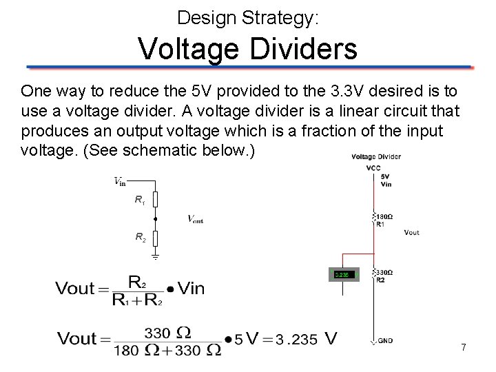
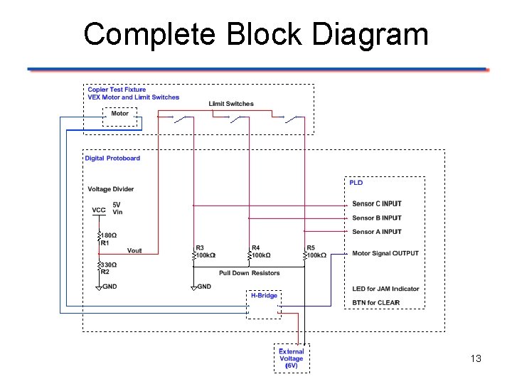
Design Strategy: Voltage Dividers One way to reduce the 5 V provided to the 3. 3 V desired is to use a voltage divider. A voltage divider is a linear circuit that produces an output voltage which is a fraction of the input voltage. (See schematic below. ) R 1 R 2 7

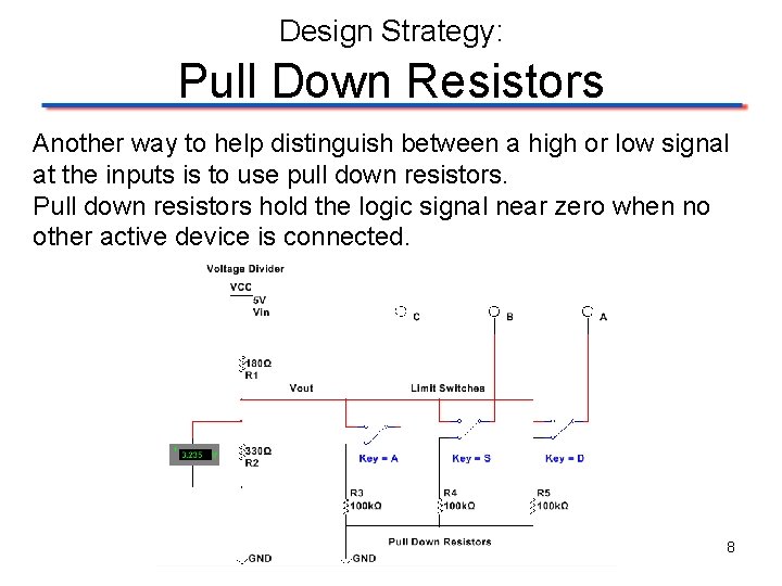
Design Strategy: Pull Down Resistors Another way to help distinguish between a high or low signal at the inputs is to use pull down resistors. Pull down resistors hold the logic signal near zero when no other active device is connected. 8

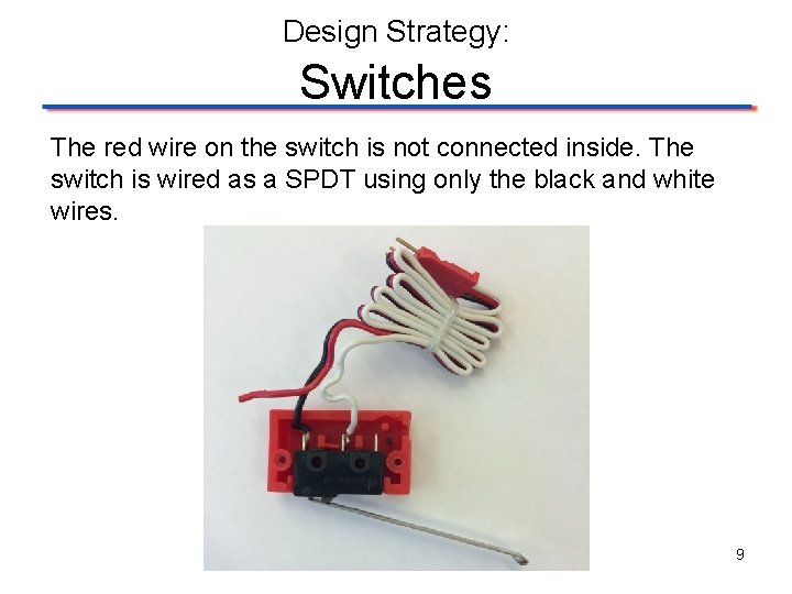
Design Strategy: Switches The red wire on the switch is not connected inside. The switch is wired as a SPDT using only the black and white wires. 9

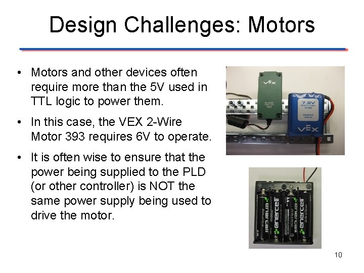
Design Challenges: Motors • Motors and other devices often require more than the 5 V used in TTL logic to power them. • In this case, the VEX 2 -Wire Motor 393 requires 6 V to operate. • It is often wise to ensure that the power being supplied to the PLD (or other controller) is NOT the same power supply being used to drive the motor. 10

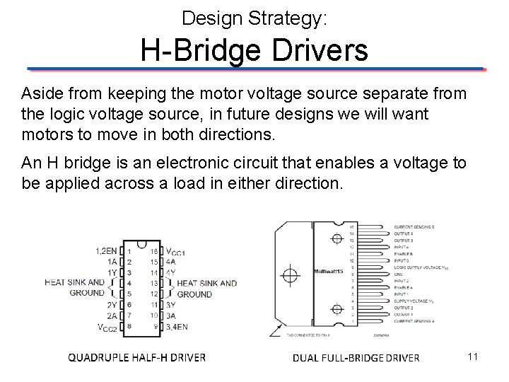
Design Strategy: H-Bridge Drivers Aside from keeping the motor voltage source separate from the logic voltage source, in future designs we will want motors to move in both directions. An H bridge is an electronic circuit that enables a voltage to be applied across a load in either direction. 11

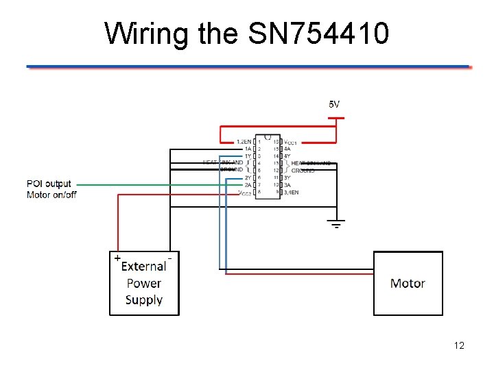
Wiring the SN 754410 12

Complete Block Diagram 13

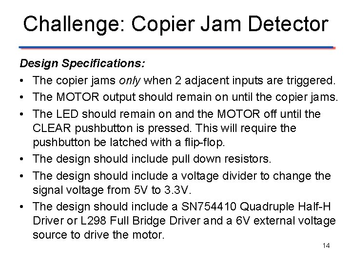
Challenge: Copier Jam Detector Design Specifications: • The copier jams only when 2 adjacent inputs are triggered. • The MOTOR output should remain on until the copier jams. • The LED should remain on and the MOTOR off until the CLEAR pushbutton is pressed. This will require the pushbutton be latched with a flip-flop. • The design should include pull down resistors. • The design should include a voltage divider to change the signal voltage from 5 V to 3. 3 V. • The design should include a SN 754410 Quadruple Half-H Driver or L 298 Full Bridge Driver and a 6 V external voltage source to drive the motor. 14

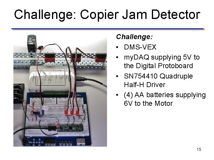
Challenge: Copier Jam Detector Challenge: • DMS-VEX • my. DAQ supplying 5 V to the Digital Protoboard • SN 754410 Quadruple Half-H Driver • (4) AA batteries supplying 6 V to the Motor 15